Table of Contents
Advertisement
Quick Links
UM3256
User manual
STM32 Nucleo-64 boards (MB1932)
Introduction
The STM32 Nucleo-64 boards, based on the MB1932 reference board (order codes
NUCLEO-U083RC
and NUCLEO-U031R8),
provide an affordable and flexible way for users to test new concepts and build prototypes with the STM32 microcontroller with
different combinations of performance, power consumption, and functionality.
®
The ARDUINO
Uno V3 connectivity support and the ST morpho headers provide an easy means of expanding the functionality
of the STM32U0 Nucleo open development platform with a wide choice of specialized shields.
The STM32 Nucleo-64 board does not require any separate probe, as it integrates the STLINK-V2EC debugger/programmer.
The STM32 Nucleo-64 board comes with the comprehensive free STM32 software libraries and examples that are available
with the
STM32CubeU0
MCU Package.
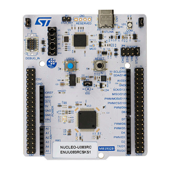
Figure 1.
NUCLEO-U083RC board (Top view)
Picture is not contractual.
UM3256 - Rev 1 - February 2024
www.st.com
For further information contact your local STMicroelectronics sales office.
Advertisement
Table of Contents

Related Manuals for ST NUCLEO-U083RC


Summary of Contents for ST NUCLEO-U083RC
-
Page 1: Figure 1. Nucleo-U083Rc Board (Top View)
® The ARDUINO Uno V3 connectivity support and the ST morpho headers provide an easy means of expanding the functionality of the STM32U0 Nucleo open development platform with a wide choice of specialized shields. The STM32 Nucleo-64 board does not require any separate probe, as it integrates the STLINK-V2EC debugger/programmer. -
Page 2: Features
Board connectors: ® – ARDUINO Uno V3 expansion connector – ST morpho extension pin headers for full access to all STM32U0 I/Os ® – USB Type-C connector for the ST-LINK – Debug_IN connector 10‑pin 1.27 mm‑pitch debug connector over STDC14/MIPI10 footprint •... -
Page 3: Ordering Information
The meaning of the codification is explained in Table Table 2. Codification explanation NUCLEO-XXYYZT Description Example: NUCLEO-U083RC MCU series in STM32 32-bit Arm Cortex MCUs STM32U0 series MCU product line in the series STM32U083 product line STM32 package pin count: 64‑pin package... -
Page 4: Development Environment
STM32 flash memory for easy demonstration of the device peripherals in standalone mode. The latest versions of the demonstration source code and associated documentation can be downloaded from www.st.com. UM3256 - Rev 1 page 4/31... -
Page 5: Conventions
UM3256 Conventions Conventions Table 3 provides the conventions used for the ON and OFF settings in the present document. Table 3. ON/OFF convention Convention Definition Jumper JPx ON Jumper fitted Jumper JPx OFF Jumper not fitted Jumper JPx [1-2] Jumper fitted between Pin 1 and Pin 2 Solder bridge SBx ON SBx connections closed by 0 Ω... -
Page 6: Quick Start
Definition Default position Comment IDD measurement STM32 VDD current measurement 5 V power selection [1-2] 5 V power supply from ST-LINK USB STLK reset No STLK reset JP6 to JP10 SWD interface On-board STLINK-V2EC debugger UM3256 - Rev 1 page 6/31... -
Page 7: Hardware Layout And Configuration
STM32 and its peripherals, such as STLINK-V2EC, push- ® buttons, LEDs, ARDUINO Uno V3 connectors, and ST morpho headers. Figure 3 shows the location of the STM32 Nucleo-64 features. The mechanical dimensions of the board are shown in Figure Figure 2. -
Page 8: Pcb Layout
User button (B2) (B1) IDD measurement (JP5) Green LED Power green (LD4) (LD3) ® ARDUINO connector (CN5) ARDUINO ® connector ST morpho headers (CN6) (CN10) STM32 microcontroller (U13) ST morpho headers (CN7) ® ARDUINO connector ® ARDUINO (CN9) connector (CN8) -
Page 9: Mechanical Drawing
UM3256 Hardware layout and configuration Mechanical drawing Figure 4. Board mechanical dimensions (in millimeters) UM3256 - Rev 1 page 9/31... -
Page 10: Embedded Stlink-V2Ec
The STLINK-V2EC programming and debugging tool is integrated with the STM32 Nucleo-64 board. For all general information concerning the debugging and programming features of STLINK-V2EC, refer to the user manual ST-LINK/V2 in-circuit debugger/programmer for STM8 and STM32 (UM1075) and the technical note Overview of ST-LINK derivatives (TN1235). -
Page 11: Programming And Debugging The On-Board Mcu Using The Debug_In Connector
UM3256 Hardware layout and configuration 6.3.3 Programming and debugging the on-board MCU using the Debug_IN connector To program the STM32 on board, plug in the Debug_IN connector (CN4), as shown in Figure 3. The Debug_IN ® ® connector is an Arm Cortex 10‑pin 1.27 mm‑pitch debug connector over STDC14/MIPI10 footprint according to Table... -
Page 12: Power Supply And Power Selection
STLK: 5 V from the STLINK-V2EC USB Type-C connector ® • VIN: 7 to 12 V from the ARDUINO or ST morpho connector, with 5 V adaptation from LDO • E5V: External 5 V power from the ST morpho connector ® •... -
Page 13: Programing And Debugging When The Power Supply Is Not From Stlink-V2Ec (Stlk)
An LDO (U11) is used to provide a fixed 5 V from VIN (7 to 12 V) E5V is the DC power coming from an external 5 V DC power source from the ST morpho connector (CN7 pin 6). The 5V jumper selection (JP4) must be on [5-6] to select the E5V power source. -
Page 14: Vdd Idd Measurement
• SB22 and SB24 OFF • R34 and R35 ON External oscillator connected to PC14 input The use of the external oscillator through pin 25 of the ST morpho connector (CN7) requests the following configuration: • SB22 ON • R34 and R35 OFF LSE not used PC14 and PC15 are used as GPIOs instead of low-speed clocks. -
Page 15: Hse: Osc Clock Supply
The STM32 Nucleo-64 reset signal is active LOW and the reset sources include: • The reset push‑button (B2) • The embedded STLINK-V2EC ® • The ARDUINO connector (CN6 pin 3) • The ST morpho connector (CN7 pin 14) UM3256 - Rev 1 page 15/31... -
Page 16: Virtual Com Port (Vcp)
STLINK-V2EC tricolor LED (LD1) The tricolor (green, orange, and red) LED provides information about STLINK-V2EC communication status (LD1). For detailed information about the LED, refer to the technical note Overview of ST-LINK derivatives (TN1235). VBUS_STLK over current LED (LD2) The red LED is ON when overcurrent is detected on USB V . -
Page 17: Jumper Configuration
SWD interface disabled and external debugger from the connector (CN4) JP2, JP3, and JP11 GND probe [1-2] 5 V from ST-LINK [3-4] 5 V from VIN 7 to 12 V 5 V power selection [5-6] 5 V from E5V [7-8]... -
Page 18: Solder Bridge Configuration
SB36 AGND is not connected to GND. PA5 controls LD4. User LED SB12 LD4 is isolated. PA13/PA14 is not connected to the ST morpho connector. SWD signals SB15/SB17 PA13/PA14 is connected to the ST morpho connector. SB23/SB44 OFF USART2 from PA2/PA3 as VCP... -
Page 19: Connectors
® • The four ARDUINO Uno V3 connectors (CN5, CN6, CN8, and CN9) • The two ST morpho connectors (CN7 and CN10) ® ARDUINO Uno V3 ® The CN5, CN6, CN8, and CN9 connectors are female connectors supporting the ARDUINO Uno V3 standard. -
Page 20: Table 10. Arduino ® Connectors On Nucleo-U083Rc And Nucleo-U031R8
® Table 10. ARDUINO connectors on NUCLEO-U083RC and NUCLEO-U031R8 Left connectors Right connectors Connector Pin number Pin name MCU pin Function Function MCU pin Pin name Pin number Connector I2C1_SCL SCL/D15 I2C1_SDA SDA/D14 VREF+ AVDD Reserved for SPI1_SCK SCK/D13 test... -
Page 21: St Morpho Connectors (Cn7 And Cn11)
STM32 Nucleo-64 board to an expansion or prototype/wrapping board placed on top of it. All signals and power pins of the STM32 are available on the two ST morpho connectors. An oscilloscope, a logic analyzer, or a voltmeter can also probe this connector. -
Page 22: Stm32 Nucleo-64 Board Information
B01. The second line shows the board serial number used for traceability. Parts marked as “ES” or “E” are not yet qualified and therefore not approved for use in production. ST is not responsible for any consequences resulting from such use. In no event will ST be liable for the customer using any of these engineering samples in production. -
Page 23: Nucleo-U083Rc And Nucleo-U031R8 Product History
UM3256 STM32 Nucleo-64 board information NUCLEO-U083RC and NUCLEO-U031R8 product history Table 12. Product history Order Product Product details Product change description Product limitations code identification MCU: • STM32U083RCT6 silicon revision "A" MCU errata sheet: • STM32U073xx and NUU083RC$KS1 Initial revision... -
Page 24: Federal Communications Commission (Fcc) And Ised Canada Compliance
UM3256 Federal Communications Commission (FCC) and ISED Canada Compliance Statements Federal Communications Commission (FCC) and ISED Canada Compliance Statements FCC Compliance Statement Part 15.19 This device complies with Part 15 of the FCC Rules. Operation is subject to the following two conditions: (1) this device may not cause harmful interference, and (2) this device must accept any interference received, including interference that may cause undesired operation. -
Page 25: Ised Compliance Statement
UM3256 Federal Communications Commission (FCC) and ISED Canada Compliance Statements ISED Compliance Statement This device complies with FCC and ISED Canada RF radiation exposure limits set forth for general population for mobile application (uncontrolled exposure). This device must not be collocated or operating in conjunction with any other antenna or transmitter. -
Page 26: Revision History
UM3256 Revision history Table 14. Document revision history Date Revision Changes 19-Feb-2024 Initial release. UM3256 - Rev 1 page 26/31... -
Page 27: Table Of Contents
ST morpho connectors (CN7 and CN11) ........ - Page 28 Product marking ............. . 22 NUCLEO-U083RC and NUCLEO-U031R8 product history ......23 Board revision history .
-
Page 29: List Of Tables
Table 10. ARDUINO connectors on NUCLEO-U083RC and NUCLEO-U031R8 ......20 Table 11. -
Page 30: List Of Figures
NUCLEO-U083RC board (Top view) ........ - Page 31 ST’s terms and conditions of sale in place at the time of order acknowledgment. Purchasers are solely responsible for the choice, selection, and use of ST products and ST assumes no liability for application assistance or the design of purchasers’...
Need help?
Do you have a question about the NUCLEO-U083RC and is the answer not in the manual?
Questions and answers