Table of Contents
Advertisement
Quick Links
UM2592
User manual
STM32WL Nucleo-64 board (MB1389)
Introduction
The
NUCLEO-WL55JC
STM32WL Nucleo-64 board, based on the MB1389 reference board (NUCLEO-WL55JC1 and
NUCLEO-WL55JC2 order codes), provides an affordable and flexible way for users to try out new concepts and build prototypes
with the STM32WL series microcontroller, choosing from the various combinations of performance, power consumption, and
features.
®
The ARDUINO
Uno V3 connectivity support and the ST morpho headers provide an easy means of expanding the functionality
of the STM32WL Nucleo open development platform with a wide choice of specialized shields.
The STM32WL Nucleo-64 board does not require any separate probe as it integrates the STLINK-V3E debugger and
programmer.
The STM32WL Nucleo-64 board is supplied with the STM32WL comprehensive software HAL library and various packaged
software examples available with the STM32CubeWL MCU Package.
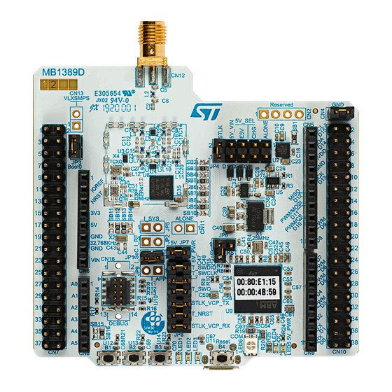
Figure 1.
NUCLEO-WL55JC top view
Figure 2.
NUCLEO-WL55JC bottom view
Pictures are not contractual.
UM2592 - Rev 3 - September 2024
www.st.com
For further information contact your local STMicroelectronics sales office.
Advertisement
Table of Contents

Related Manuals for ST NUCLEO-WL55JC


Summary of Contents for ST NUCLEO-WL55JC
-
Page 1: Figure 1. Nucleo-Wl55Jc Top View
® The ARDUINO Uno V3 connectivity support and the ST morpho headers provide an easy means of expanding the functionality of the STM32WL Nucleo open development platform with a wide choice of specialized shields. The STM32WL Nucleo-64 board does not require any separate probe as it integrates the STLINK-V3E debugger and programmer. -
Page 2: Features
® – ARDUINO Uno V3 expansion connector – ST morpho extension pin headers for full access to all STM32WL I/Os • Delivered with SMA antenna • Flexible power-supply options: ST-LINK USB V , USB connector, or external sources •... -
Page 3: Ordering Information
UM2592 Ordering information Ordering information To order an STM32WL Nucleo-64 board, refer to Table 1. Additional information is available from the datasheet and reference manual of the target STM32. Table 1. List of available products Board Order code Target STM32 Differentiating feature reference High-frequency band. -
Page 4: Development Environment
STM32 flash memory for easy demonstration of the device peripherals in standalone mode. The latest versions of the demonstration source code and associated documentation can be downloaded from www.st.com. UM2592 - Rev 3 page 4/51... -
Page 5: Conventions
UM2592 Conventions Conventions Table 3 provides the conventions used for the ON and OFF settings in the present document. Table 3. ON/OFF convention Convention Definition Jumper JPx ON Jumper fitted Jumper JPx OFF Jumper not fitted Jumper JPx [1-2] Jumper fitted between Pin 1 and Pin 2 Solder bridge SBx ON SBx connections closed by 0 Ω... -
Page 6: Quick Start
– For a list of available regions run AT_LIST_REGIONS. 5. Then the concentrator (a second NUCLEO-WL55JC) starts flashing a green LED on each time slot of the network. 6. To get the demonstration fully up and running, up to 14 Nucleo demonstration sensors can be flashed and placed against a Nucleo demonstration concentrator. - Page 7 Comment For STM32WL current I_SYS OFF (SB27 ON) measurements (digital part) STLK-RST STLINK-V3E reset 5V_PWR 5 V power-source selection T_SWDIO connected to ST- [1-2] LINK T_SWCLK connected to ST- [3-4] LINK [5-6] T_SWO connected to ST-LINK Signals between STLINK-V3E and...
-
Page 8: Hardware Layout And Configuration
Figure 3 shows the connections between the STM32 and its peripherals (STLINK-V3E, push-buttons, LEDs, USB, ® ARDUINO Uno, and ST morpho headers). Figure 4 Figure 6 show the location of these features on the STM32WL Nucleo-64 board. The mechanical dimensions of the board are shown in Figure Figure 3. -
Page 9: Pcb Layout
UM2592 Hardware layout and configuration PCB layout Figure 4. Top layout Two stickers are on the top of the MB1389 board: one RF certification sticker and one UID64 sticker. 1. The RF certification sticker is mandatory for any boards containing an RF module as this Nucleo MB1389, which contains a LoRa/SigFox RF transceiver. -
Page 10: Figure 5. Rf Certification And Uid64 Stickers
UM2592 Hardware layout and configuration Figure 5 shows both stickers: Figure 5. RF certification and UID64 stickers UM2592 - Rev 3 page 10/51... -
Page 11: Figure 6. Bottom Layout
UM2592 Hardware layout and configuration Figure 6. Bottom layout UM2592 - Rev 3 page 11/51... -
Page 12: Mechanical Drawing
UM2592 Hardware layout and configuration Mechanical drawing Figure 7. STM32WL Nucleo 73 board mechanical drawing (in millimeters) Embedded STLINK-V3E There are two different ways to program and debug the onboard STM32 MCU: • Using the embedded STLINK-V3E • Using an external debug tool connected to the MIPI10 connector (CN16). The STLINK-V3E programming and debugging tool is integrated into the STM32WL Nucleo-64 board. -
Page 13: Drivers
STLINK-V3E product (for example new functionalities, bug fixes, support for new microcontroller families). It is recommended to visit the www.st.com website before starting to use the STM32WL Nucleo-64 board and periodically, to stay up to date with the latest firmware version. -
Page 14: Table 5. Mipi10/Jtagstdc14 Debug Connector (Cn16)
UM2592 Hardware layout and configuration Figure 9. Connecting an external debug tool to program the on-board STM32WL Table 5. MIPI10/JTAGSTDC14 debug connector (CN16) MIPI10 pin STDC14 pin CN16 Function Reserved Reserved Target VCC T_JTMS target SWDIO using SWD protocol or target JTMS using T_SWDIO JTAG protocol Ground... -
Page 15: Power Supply
UM2592 Hardware layout and configuration Power supply Six different sources can provide the power supply: • A host PC connected to CN1 through a USB cable (default setting) • An external VIN from 7 to 12 V power supply connected to CN7 pin 24 •... -
Page 16: Figure 10. Stm32Wl Nucleo-64 Board Power Tree
EN-60950-1: 2006+A11/2009 standard and must be Safety Extra Low Voltage (SELV) with limited power capability. If the power supply is 3V3 or STD_ALONE_5V, the ST-LINK is not powered and cannot be used. UM2592 - Rev 3... -
Page 17: Figure 11. Power Supply Input From Stlink-V3E Usb Connector With Pc (5 V, 500 Ma Maximum)
500 mA occurs on board, the red LED (LED4) is lit. The Nucleo board and its shield can be powered from the ST-LINK USB connector (CN1), but only the ST-LINK circuit gets power before USB enumeration because the host PC only provides 100 mA to the board at that time. -
Page 18: Table 6. External Power Sources: Vin (7 To 12 V)
UM2592 Hardware layout and configuration Caution: If the maximum current consumption of the STM32WL Nucleo-64 board and its shield boards exceeds 300 mA, it is mandatory to check the root cause of the overconsumption. Consequently, if needed, power the STM32WL Nucleo-64 board with an external power supply connected to VIN, 5 V, or 3.3 V. -
Page 19: Table 7. External Power Sources: E5V (5 V)
UM2592 Hardware layout and configuration Figure 12. Power supply input from VIN (7 to 12 V, 800 mA maximum) External power supply input from E5V (5 V, 500 mA maximum) When E5V power supplies the STM32WL Nucleo-64 board (refer to Table 7 Figure 13), the jumper... -
Page 20: Table 8. External Power Sources: 5V_Chgr (5 V)
UM2592 Hardware layout and configuration Figure 13. Power supply input from 5V_EXT (5 V, 500 mA maximum) External power supply input from 5 V USB charger When a USB charger on CN1 power supplies the STM32WL Nucleo-64 board (refer to Table 8 Figure 14),... -
Page 21: Table 9. External Power Sources: 3V3
Hardware layout and configuration Figure 14. Power supply input from ST-LINK USB connector with 5 V USB charger External power supply input from external 3.3 V When a shield board provides the 3.3 V, it is interesting to use the 3.3 V (CN6 pin 4 or CN7 pin 16) directly as... -
Page 22: Table 10. External Power Sources: Std_Alone_5V
UM2592 Hardware layout and configuration Figure 15. Power supply input from external 3V3 External power supply input STD_ALONE_5V (5 V, 500 mA maximum) When STD_ALONE_5V power supplies the STM32WL Nucleo-64 board (refer to Table 10 Figure 16), the jumper configuration must be on ALONE (JP4 [9‑10]). Table 10. -
Page 23: Figure 16. Power Supply Input From Std_Alone_5V (5 V, 500 Ma Maximum)
UM2592 Hardware layout and configuration Figure 16. Power supply input from STD_ALONE_5V (5 V, 500 mA maximum) When the board is supplied with STD_ALONE_5V (on connector 11), then the STLINK-V3E debugger is not supplied. Take care to supply correctly the board when using CN11. CN11 pin 1 is the STD_ALONE_5V supply and pin 2 is the GND, as shown in Figure Figure 17. -
Page 24: Debugging While Using Vin Or Ext As An External Power Supply
Debugging while using VIN or EXT as an external power supply When VIN or E5V powers the board, it is still possible to use ST-LINK to program or debug, but it is mandatory to power the board first using VIN or EXT, then connect the USB cable to the PC. In this way, the enumeration succeeds, thanks to the external power source. -
Page 25: Lse Clock (Low-Speed External Clock) - 32.768 Khz
USB power fault (OC, overcurrent) (LED4) LED4 indicates that the board power consumption on the ST-LINK USB exceeds 500 mA. As a consequence, the user must check the root cause of the overconsumption or power of the board using an external power supply. -
Page 26: Push-Buttons
UM2592 Hardware layout and configuration 6.6.2 Push-buttons B1 (USER) The user button is connected to the STM32WL I/O PA0 by default (WKUP1, SB16 ON, and SB15 OFF) or PC13 (WKUP2, SB15 ON, and SB16 OFF) of the STM32WL microcontroller. B2 (USER) The user button is connected to the STM32WL I/O PA1 of the STM32WL microcontroller. -
Page 27: Current Consumption Measurement (I_Soc)
UM2592 Hardware layout and configuration Figure 18. RF block diagram VDD_RF VDDSMPS VDDRF SMPS part VLXSMPS Power management VFBSMPS PB0-VDD_TCXO STM32 WL transceiver VDDRF1V55 switch VDDPA TCXO Reg PA VR_PA FE_CTRL1 switch OSC_IN RF Tx HP path Xtal Tx HP PA HP matching RFO_HP... -
Page 28: Virtual Com Port (Vcp): Lpuart And Usart
The STM32WL Nucleo-64 board offers the possibility to select which USART interface is connected to the ® STLINK-V3E, ARDUINO Uno V3 connector (CN9 pins 2 and 1), or to the ST morpho connector (CN10 pins 35 and 37). The selection is done by setting the related solder bridges as detailed in... -
Page 29: Table 12. Lpuart1 Connection
SB2, SB4, SB6, SB10: OFF SB2, SB4: ON ® LPUART1 (PA2/PA3) connected to the ARDUINO (D1 and D0) and ST morpho connector (CN10 pin 35 and 37). SB3, SB5, SB7, SB9: OFF 1. The default configuration is shown in bold By default: •... -
Page 30: Solder Bridges
STLINK_RX (T_VCP_RX) connected to USART1 Rx PB7 USART1 Rx SB10 STLINK_RX (T_VCP_RX) not connected to USART1 Rx PC14-OSC32_IN connected to ST morpho connector I/O usage (CN7 pin 25) SB11 PC14-OSC32_IN not connected to ST morpho connector LSE provided by external LSE 32.768kHz CLK X2... - Page 31 BOOT0/PH3 connected to ST morpho connector CN7 pin BOOT0/PH3 on ST morpho SB19 connector BOOT0/PH3 not connected to ST morpho connector CN7 pin 32 MHz TCXO supplied by PB0-VDD_TCXO (to STM32WL) 32 MHz TCXO supply SB20 32 MHz TCXO disconnected to PB0-VDD_TCXO (to...
-
Page 32: Board Connectors
UM2592 Board connectors Board connectors Several connectors are implemented on the STM32WL Nucleo-64 board. STLINK-V3E USB Micro-B connector (CN1) The USB Micro-B connector (CN1) is used to connect the embedded STLINK-V3E to a PC for programming and debugging purposes. Figure 20. USB Micro-B connector (CN23) front view Table 14. -
Page 33: Sma Connector (Cn12)
UM2592 Board connectors Table 15. MIPI10 connector (CN16) pinout (STDC14 pinout compatible) Connector Pin number Description Pin number Description VDD (3V3) T_SWDIO (PA13) T_SWCLK (PA14) KEY (connected to GND) T_SWO (PB3) CN16 T_JTDI (PA15) GNDDetect (connected to GND through T_NRST a 100 Ω... -
Page 34: Arduino ® Uno V3 Connector (Cn5, Cn6, Cn8, And Cn9)
UM2592 Board connectors ® ARDUINO Uno V3 connector (CN5, CN6, CN8, and CN9) ® CN5, CN6, CN8, and CN9 are female connectors compatible with the ARDUINO standard. Refer to Figure 23 ® their location. Most shields designed for ARDUINO can fit with the STM32WL Nucleo-64 board. ®... -
Page 35: Table 17. Arduino ® Connector Pinout
UM2592 Board connectors ® Table 17. ARDUINO connector pinout Connector Pin number Pin name Signal name STM32 pin Function Reserved for test IOREF I/O reference NRST T_NRST NRST RESET 3.3 V input/output 5 V output 7 to 12 V input power ADC1_IN5 ADC1_IN4 PA10... -
Page 36: St Morpho Connectors (Cn7 And Cn10)
ST morpho connectors (CN7 and CN10) The ST morpho (CN7 and CN10) connectors are male pin headers accessible on both sides of the board. All signals and power pins of the STM32WL MCU are available on the ST morpho connectors. An oscilloscope, logical analyzer, or voltmeter can also probe these connectors. - Page 37 UM2592 Board connectors CN7 odd pins CN7 even pins CN10 odd pins CN10 even pins Pin name Pin name Pin name Pin name number number number number NRST PA13 PA14 PA15 PC13 PC14 PB10 PC15 PB15 PB11 PA10 AGND VBAT PB12 PB14 PB6/PA2...
-
Page 38: Stm32Wl Nucleo-64 I/O Assignment
UM2592 STM32WL Nucleo-64 I/O assignment STM32WL Nucleo-64 I/O assignment Table 19. STM32WL Nucleo-64 I/O assignment Pin name Signal or label Main/optional feature/(SB) VSSSMPS VSSSMPS GND of LDO/SMPS step-down converter External power supply of LDO/SMPS step-down VDDSMPS VDDSMPS converter PA14 T_SWCLK T_SWCLK VDDA VDDA... - Page 39 UM2592 STM32WL Nucleo-64 I/O assignment Pin name Signal or label Main/optional feature/(SB) PB12 PB12 ARD_D2 - I/O ARD_A0 - ADC1_IN5 VDDRF VDDRF VDD supply for the RF part VDD voltage supply ARD_D7 - I/O FE_CTRL1 ARD_D12 - SPI1_MISO NRST T_NRST STM32WL RESET PB0-VDD_TCXO PB0-VDD_TCXO...
-
Page 40: Stm32Wl Nucleo-64 Board Product Information
B01. The second line shows the board serial number used for traceability. Parts marked as “ES” or “E” are not yet qualified and therefore not approved for use in production. ST is not responsible for any consequences resulting from such use. In no event will ST be liable for the customer using any of these engineering samples in production. -
Page 41: Stm32Wl Nucleo-64 Board Product History
UM2592 STM32WL Nucleo-64 board product information STM32WL Nucleo-64 board product history Table 20. Product history Order Product Product details Product change description Product limitations code identification MCU: • STM32WL55JCI7 silicon revision "Z" MCU errata sheet: • STM32WL55xx, NUWL55JC1$CT1 Initial revision No limitation STM32WL54xx device errata (ES0500) -
Page 42: Board Revision History
UM2592 STM32WL Nucleo-64 board product information Order Product Product details Product change description Product limitations code identification MCU: • STM32WL55JCI7 silicon revision "Y" MCU errata sheet: • MCU silicon revision changed • STM32WL55xx, NUWL55JC2$CT2 No limitation • Main board revision changed STM32WL54xx device errata (ES0500) Board:... -
Page 43: Federal Communications Commission (Fcc) And Ised Canada Compliance
UM2592 Federal Communications Commission (FCC) and ISED Canada Compliance Statements Federal Communications Commission (FCC) and ISED Canada Compliance Statements 10.1 FCC Compliance Statement Part 15.19 This device complies with Part 15 of the FCC Rules. Operation is subject to the following two conditions: (1) this device may not cause harmful interference, and (2) this device must accept any interference received, including interference that may cause undesired operation. -
Page 44: Ised Compliance Statement
UM2592 Federal Communications Commission (FCC) and ISED Canada Compliance Statements 10.2 ISED Compliance Statement This device complies with FCC and ISED Canada RF radiation exposure limits set forth for general population for mobile application (uncontrolled exposure). This device must not be collocated or operating in conjunction with any other antenna or transmitter. -
Page 45: 11 Déclaration De Conformité Ce Simplifiée
Le soussigné, STMicroelectronics, déclare que l'équipement radioélectrique du type Nucleo MB1389D est conforme à la directive 2014/53/UE. Le texte complet de la déclaration UE de conformité est disponible à l'adresse internet suivante: www.st.com. Bande de fréquence utilisée en transmission et puissance max rayonnée dans ces bandes : Bande de fréquence : 865 MHz / 870 MHz... -
Page 46: Revision History
Chapter on antenna stuck to SMA connector as FCC constraint in Section 6.6.3 Updated: 9-Jul-2021 ® • Table 17 in Section 7.4: CN5, CN6, CN8, and CN9: ARDUINO Uno V3 connector • NUCLEO-WL55JC product history • Board revision history Updated Product marking. 27-Sep-2024 Added Product history Board revision history tables. -
Page 47: Table Of Contents
UM2592 Contents Contents Features................2 Ordering information . - Page 48 ST morpho connectors (CN7 and CN10) ........
-
Page 49: List Of Tables
Pin assignment of the ST morpho connectors ........ -
Page 50: List Of Figures
Power supply input from ST-LINK USB connector with 5 V USB charger ......21... - Page 51 ST’s terms and conditions of sale in place at the time of order acknowledgment. Purchasers are solely responsible for the choice, selection, and use of ST products and ST assumes no liability for application assistance or the design of purchasers’...
Need help?
Do you have a question about the NUCLEO-WL55JC and is the answer not in the manual?
Questions and answers