Table of Contents
Advertisement
Quick Links
UM2581
User manual
STM32L5 Nucleo-144 board (MB1361)
Introduction
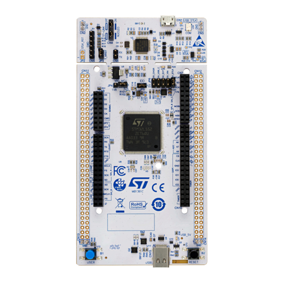
The STM32L5 Nucleo-144 board based on the MB1361 reference board (NUCLEO-L552ZE-Q) provides an affordable and
flexible way for users to try out new concepts and build prototypes by choosing from the various combinations of performance
and power consumption features, provided by the STM32L5 microcontroller.
®
The ST Zio connector, which extends the ARDUINO
Uno V3 connectivity, and the ST morpho headers provide easy expansion
of the functionality of the STM32 Nucleo open development platform with a wide choice of specialized shields.
The STM32L5 Nucleo-144 board does not require any separate probe as it integrates the ST-LINK/V2-1 debugger/programmer.
The STM32L5 Nucleo-144 board comes with the STM32 comprehensive free software libraries and examples available with the
STM32CubeL5
MCU Package.
Figure 1.
STM32L5 Nucleo-144 board
Picture is not contractual.
UM2581 - Rev 2 - January 2020
www.st.com
For further information contact your local STMicroelectronics sales office.
Advertisement
Table of Contents

Related Manuals for ST STM32L5 Nucleo-144 board


Summary of Contents for ST STM32L5 Nucleo-144 board
-
Page 1: Figure 1. Stm32L5 Nucleo-144 Board
STM32 Nucleo open development platform with a wide choice of specialized shields. The STM32L5 Nucleo-144 board does not require any separate probe as it integrates the ST-LINK/V2-1 debugger/programmer. The STM32L5 Nucleo-144 board comes with the STM32 comprehensive free software libraries and examples available with the STM32CubeL5 MCU Package. -
Page 2: Features
ST morpho expansion connector • Flexible power-supply options: ST-LINK, USB V or external sources • On-board ST-LINK/V2-1 debugger/programmer with USB re-enumeration capability: mass storage, Virtual COM port, and debug port • Comprehensive free software libraries and examples available with the STM32CubeL5 MCU Package ™... -
Page 3: Ordering Information
Evaluation tools marked as “ES” or “E” are not yet qualified and therefore not ready to be used as reference design or in production. Any consequences deriving from such usage will not be at ST charge. In no event, ST will be liable for any customer usage of these engineering sample tools as reference designs or in production. -
Page 4: Development Environment
STM32 Flash memory for easy demonstration of the device peripherals in standalone mode. The latest versions of the demonstration source code and associated documentation can be downloaded from www.st.com. UM2581 - Rev 2 page 4/48... -
Page 5: Conventions
UM2581 Conventions Conventions Table 3 provides the conventions used for the ON and OFF settings in the present document. Table 3. ON/OFF convention Convention Definition Jumper JPx ON Jumper fitted Jumper JPx OFF Jumper not fitted Jumper JPx [1-2] Jumper should be fitted between Pin 1 and Pin 2 Solder bridge SBx ON SBx connections closed by 0 Ω... -
Page 6: Quick Start
Connect the STM32L5 Nucleo-144 board to a PC with a USB cable (Type-A to Micro-B) through the USB connector CN1 to power the board. Then, the green LED LD6 (5V_PWR) lights up, LD4 (COM) and green LED LD1 blink. -
Page 7: Figure 2. Default Board Configuration
UM2581 Default board configuration Figure 2. Default board configuration UM2581 - Rev 2 page 7/48... -
Page 8: Hardware Layout And Configuration
LEDs, USB, ST Zio connectors and ST morpho headers). Figure 4 Figure 5 show the location of these features on the STM32L5 Nucleo-144 board. The mechanical dimensions of the board are shown in Figure Figure 3. Hardware block diagram ST-LINK/V2.1 Part... -
Page 9: Figure 4. Stm32L5 Nucleo-144 Board Top Layout
UM2581 STM32L5 Nucleo-144 board layout STM32L5 Nucleo-144 board layout Figure 4. STM32L5 Nucleo-144 board top layout UM2581 - Rev 2 page 9/48... -
Page 10: Figure 5. Stm32L5 Nucleo-144 Board Bottom Layout
UM2581 STM32L5 Nucleo-144 board layout Figure 5. STM32L5 Nucleo-144 board bottom layout UM2581 - Rev 2 page 10/48... -
Page 11: Mechanical Drawing
UM2581 Mechanical drawing Mechanical drawing Figure 6. STM32L5 Nucleo-144 board mechanical drawing (in millimeter) UM2581 - Rev 2 page 11/48... -
Page 12: Embedded St-Link/V2-1
, is found at www.st.com. In case the STM32L5 Nucleo-144 board is connected to the PC before the driver is installed, some STM32L5 Nucleo-144 interfaces may be declared as “Unknown” in the PC device manager. In this case, the user must... -
Page 13: Nucleo St-Link/V2-1 Hardware Configuration
UM2581 Embedded ST-LINK/V2-1 6.3.3 NUCLEO ST-LINK/V2-1 hardware configuration The embedded ST-LINK/V2-1 can be used in two different ways according to the jumper states, refer to Table 5 for setting, depending on the configuration: • Program/debug the MCU on-board • Program/debug an MCU in an external application board using a cable connected to SWD connector Table 5. -
Page 14: Table 6. Debug Connector Swd: Pinning
Embedded ST-LINK/V2-1 6.3.3.2 Using the ST-LINK/V2-1 to program and debug an external STM32 application It is easy to use the ST-LINK/V2-1 to program the STM32 on an external application. Simply remove the two jumpers from CN4, as shown in Figure... -
Page 15: Power Supply
JP5 pin 2 5V_STLK is a DC power with limitation from ST-LINK USB connector (USB Type Micro-B connector of ST-LINK/ V2-1). In this case, the JP6 jumper must be on pin [1-2] to select the 5V_STLK power source on the JP6 silkscreen. -
Page 16: Figure 10. Jp6 [1-2]: 5V_Stlk Power Source
Power supply Nucleo board with its shield can be powered from ST-LINK USB connector CN1, but only the ST-LINK circuit has the power before USB enumeration because the host PC only provides 100 mA to the board at that time. During the USB enumeration, the Nucleo board asks for the 500mA power to the host PC. -
Page 17: Figure 11. Jp6 [3-4]: 5V_Vin Power Source
-included Zio connector, CN8 pin 15 named VIN on the connector silkscreen, or from the ST morpho connector CN11 pin 24. In this case, the JP6 jumper must be on pin [3-4] to select the 5V_VIN power source on the JP6 silkscreen. In that case, the DC power comes from the ®... -
Page 18: Figure 12. Jp6 [5-6]: 5V_Ext Power Source
UM2581 Power supply Figure 12. JP6 [5-6]: 5V_EXT Power source ™ 5V_USB_C is the DC power supply connected to the user USB Type-C (CN15). In this case, to select the 5V_USB_TYPE_C power source on the JP6 silkscreen, the jumper must be on pins [7-8]. 5V_USB_C configuration: Jumper JP6 [7-8] must be connected as shown in Figure UM2581 - Rev 2... -
Page 19: Figure 13. Jp6 [7-8]: 5V_Usb_C Power Source
JP6 [7-8]: 5V_USB_C Power source 5V_CHGR is the DC power charger connected to USB ST-LINK (CN1). To select the 5V_USB_CHARGER power source on the JP6 silkscreen, the jumper must be on pins [9-10]. In this case, if an external USB charger powers the Nucleo board, then the debug is not available. -
Page 20: Figure 14. Jp6 [9-10]: 5V_Chgr Power Source
Caution: A solder bridge (SB1) can be used to bypass the USB PWR protection switch. (This is not an ST recommended setting). SB1 can be set only in the case when the PC USB powers the board and maximum current ®... -
Page 21: Programing/Debugging When The Power Supply Is Not From St-Link (5V_Stlk)
JP5 pin 2) directly as power input, for instance in case the 3V3 is provided by an extension board. When Nucleo is powered by 3V3, the ST-LINK is not powered thus programming and debug features are unavailable. Two different configurations are possible to use 3V3 to power the board: •... -
Page 22: Leds
A green user LED is connected to the STM32 I/O PA5 (SB120 ON and SB118 OFF, optional configuration corresponding to the ST Zio D13) or PC7 (SB120 OFF and SB118 ON, default configuration). A transistor is used to drive the LED when the I/O voltage is 1V8. -
Page 23: Push-Buttons
UM2581 Push-buttons LD6 PWR The green LED indicates that the STM32 part is powered by a 5V source, and this source is available on CN8 pin 9 and CN11 pin 18. ™ LD7 USB Type-C This green LED is driven by the presence of the 5V_USB_TYPEC. Refer to Section 6.13.1 USB FS device more details. -
Page 24: Osc Clock Sources
LSE is the 32.768 kHz crystal for the STM32 embedded RTC. • MCO is the 8 MHz clock from ST-LINK MCU for the STM32 microcontroller. • HSE is the 16 MHz oscillator for the STM32 microcontroller. This clock is not implemented in a basic configuration. -
Page 25: Reset Sources
MCO from ST-LINK (Default: not connected): MCO, the output of ST-LINK MCU, is used as an input clock. This frequency cannot be changed. It is fixed at 8 MHz, and connected to PH0 OSC_IN of STM32 microcontroller. The following configuration is needed: •... -
Page 26: Boot From Rss
CN11 pin 5 (VDD) and 7 (PH3_BOOT0). 6.12 Virtual COM port: LPUART or USART An LPUART or a USART interface of STM32 microcontroller on NUCLEO board can be connected to ST-LINK/ ® V2-1 MCU or on shields on ST morpho connectors and ARDUINO Uno V3 connectors. -
Page 27: Usb Type-C ™ Fs
UM2581 USB Type-C™ FS By default: • Communication between target MCU and ST-LINK MCU is enabled on LPUART1. ® • Communication between target MCU, ARDUINO and ST morpho connectors is enabled on USART3, not to interfere with the VCP interface. -
Page 28: Usb Type-C™ Connector
UM2581 USB Type-C™ FS ™ • fault detection: UCPD_FLT: This signal is provided by the STM USB Type-C port protection. It is used as fault reporting to MCU after a bad V level detection. By design, the STM32 Nucleo-144 V protection is set to 6 V max. -
Page 29: Jumper Configuration
ST-LINK MCU STLK_RST Normal mode ST-LINK able to reset target MCU T_NRST ST-LINK not able to reset target MCU configuration to use when CN5 is used with external application ON [1-2] VDD_MCU voltage selection = 3V3 VDD_MCU voltage selection... -
Page 30: Solder Bridge Configuration
UM2581 Solder bridge configuration 6.15 Solder bridge configuration Table 16 details the solder bridges of the STM32L5 Nucleo-144 board. Table 16. SB configuration (1)(2) Definition Bridge Setting Comment USB power switch protection enable ST-LINK USB Power bypass mode USB power switch by-passed (not recommended) - Page 31 UM2581 Solder bridge configuration Definition Bridge (1)(2) Comment Setting PB5 not connected to Zio CN7 for SPI_B interface: Reserved for UCPD_DBn SB135 PB5 connected to Zio CN7 for SPI_B interface, can’t be used for UCPB_DBn AGND AGND connected to GND. Reserved, do not modify. SWD interface SB100/SB102/ Reserved, do not modify...
- Page 32 UM2581 Solder bridge configuration Definition Bridge (1)(2) Comment Setting SB134 PB4 connected to Zio CN7 for SAI_D interface PB4 not connected to Zio CN7 for SPI_B interface SB139 PB4 connected to Zio CN7 for SPI_B interface Zio SAI_D / SPI_B interface PB5 not connected to Zio CN7 for SPI_B interface: Reserved for UCPD_DB1...
- Page 33 UM2581 Solder bridge configuration Definition Bridge (1)(2) Comment Setting VDDA input not supplied by VDD_MCU MCU VDDA SB150 VDDA input connected to VDD_MCU (SBN149 must be not connected) PB10 not used as QSPI_CLK SB151 PB10 used as QSPI_CLK PB10 I/O selection PB10 not used as TIMER for Motor Control SB157 PB10 used as TIMER for Motor Control...
-
Page 34: Extension Connectors
UM2581 Extension connectors Extension connectors Six extension connectors are implemented on the STM32L5 Nucleo-144 board: ® • CN7, CN8, CN9, and CN10 for Zio connector supporting ARDUINO Uno V3 • CN11 and CN12 for ST morpho connector The jumpers for voltage selection and IDD measurements are not described here. -
Page 35: Table 17. Pinout Of Arduino ® -Included Zio Connector Cn7
UM2581 Zio connectors supporting ARDUINO® Uno V3 ® Table 17. Pinout of ARDUINO -included Zio connector CN7 STM32 STM32 Pin name Signal name Pin name Signal name function function SAI_C_MCLK SAI2_A I2C_A_SCL I2C1 SAI_C_SD PD11 SAI2_A I2C_A_SDA I2C1 SAI_C_SCK PB13 SAI2_A VREFP SAI_C_FS... -
Page 36: Table 20. Pinout Of Arduino ® -Included Zio Connector Cn10
UM2581 Zio connectors supporting ARDUINO® Uno V3 STM32 STM32 Signal name Signal name names function names function ADC12_IN USART_B_CTS USART2 ADC12_IN COMP1_INP COMP1 SAI_A_MCLK SAI1_A COMP2_INP COMP2 SAI_A_FS SAI1_A I2C_B_SMBA I2C2 SAI_A_SCK SAI1_A I2C_B_SCL I2C2 SAI_A_SD SAI1_A I2C_B_SDA I2C2 SAI_B_SD SAI1_B SAI_B_SCK SAI1_B... -
Page 37: St Morpho Connector Cn11 And Cn12
STM32 Nucleo-144 board to an extension board or a prototype/wrapping board placed on top of the STM32 Nucleo-144 board. All signals and power pins of the STM32 are available on the ST morpho connector. An oscilloscope, a logic analyzer or a voltmeter can also probe this connector. -
Page 38: Table 21. Pin Assignment Of The St Morpho Connector
UM2581 ST morpho connector CN11 and CN12 Table 21 shows the pin assignments for the STM32 on the ST morpho connector. Table 21. Pin assignment of the ST morpho connector CN11 odd pins CN11 even pins CN12 odd pins CN12 even pins... - Page 39 REFP 3. 5V_STLK is the 5V power signal, coming from the ST-LINK/V2-1 USB connector. It rises before the 5V signal of the board. 4. PA13 and PA14 are shared with SWD signals connected to ST-LINK/V2-1. If the ST-LINK part is not cut, it is not recommended to use them as I/O pins.
-
Page 40: Limitation
UM2581 Limitation Limitation RSS/bootloader limitation Issue observed: The STM32L5 part soldered on NUCLEO-L552ZE-Q that embeds the bootloader V9.0 is affected by the limitations described in Section 6.11 RSS/bootloader. Proposed workaround: Refer to Section 6.11 RSS/bootloader to detail workaround. Parts impacted: This applies only to the NUCLEO-L552ZE-Q with the finished good (FG) NUL552ZEQ$AU1 (Sticker available on the top side of the board). -
Page 41: Federal Communications Commission (Fcc) And Industry Canada (Ic) Compliance
UM2581 Federal Communications Commission (FCC) and Industry Canada (IC) Compliance Statements Federal Communications Commission (FCC) and Industry Canada (IC) Compliance Statements FCC Compliance Statement Part 15.19 This device complies with Part 15 of the FCC Rules. Operation is subject to the following two conditions: (1) this device may not cause harmful interference, and (2) this device must accept any interference received, including interference that may cause undesired operation. -
Page 42: Ce Conformity
UM2581 CE conformity CE conformity 10.1 Warning EN 55032 / CISPR32 (2012) Class B product Warning: this device is compliant with Class B of EN55032 / CISPR32. In a residential environment, this equipment may cause radio interference. Avertissement : cet équipement est conforme à la Classe B de la EN55032 / CISPR 32. Dans un environnement résidentiel, cet équipement peut créer des interférences radio. -
Page 43: Revision History
UM2581 Revision history Table 22. Document revision history Date Version Changes 30-Sep-2019 Initial release Added: • Section 8 Limitation Updated: 28-Jan-2020 • Section 6.11 RSS/bootloader • Section 9 Section 10 switched to Class B • Table 20 UM2581 - Rev 2 page 43/48... -
Page 44: Table Of Contents
6.3.3 NUCLEO ST-LINK/V2-1 hardware configuration ....... . 12 Power supply ..............15 6.4.1... - Page 45 ST morpho connector CN11 and CN12 ........
-
Page 46: List Of Tables
Pin assignment of the ST morpho connector ........ -
Page 47: List Of Figures
STM32L5 Nucleo-144 board mechanical drawing (in millimeter) ....... . . - Page 48 ST’s terms and conditions of sale in place at the time of order acknowledgement. Purchasers are solely responsible for the choice, selection, and use of ST products and ST assumes no liability for application assistance or the design of Purchasers’...
Need help?
Do you have a question about the STM32L5 Nucleo-144 board and is the answer not in the manual?
Questions and answers