Sign In
Upload
Manuals
Brands
ST Manuals
Motherboard
NUCLEO-WL55JC STM32WL
ST NUCLEO-WL55JC STM32WL Manuals
Manuals and User Guides for ST NUCLEO-WL55JC STM32WL. We have
2
ST NUCLEO-WL55JC STM32WL manuals available for free PDF download: User Manual
ST NUCLEO-WL55JC STM32WL User Manual (51 pages)
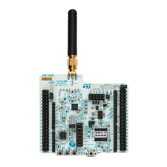
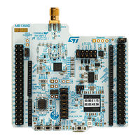
STM32WL Nucleo-64 board (MB1389)
Brand:
ST
| Category:
Computer Hardware
| Size: 9 MB
Table of Contents
Figure 1. NUCLEO-WL55JC Top View
1
Figure 2. NUCLEO-WL55JC Bottom View
1
Features
2
Ordering Information
3
Codification
3
Table 1. List of Available Products
3
Table 2. Codification Explanation
3
Development Environment
4
System Requirements
4
Development Toolchains
4
Demonstration Software
4
Conventions
5
Table 3. ON/OFF Convention
5
Quick Start
6
Getting Started
6
Table 4. Jumper Configuration
6
Hardware Layout and Configuration
8
Figure 3. Hardware Block Diagram
8
PCB Layout
9
Figure 4. Top Layout
9
Figure 5. RF Certification and UID64 Stickers
10
Figure 6. Bottom Layout
11
Mechanical Drawing
12
Embedded STLINK-V3E
12
Figure 7. STM32WL Nucleo 73 Board Mechanical Drawing (in Millimeters)
12
Drivers
13
STLINK-V3E Firmware Upgrade
13
Using an External Debug Tool to Program and Debug the On-Board STM32
13
Figure 8. USB Composite Device
13
Table 5. MIPI10/JTAGSTDC14 Debug Connector (CN16)
14
Figure 9. Connecting an External Debug Tool to Program the On-Board STM32WL
14
Power Supply
15
Figure 10. STM32WL Nucleo-64 Board Power Tree
16
Figure 11. Power Supply Input from STLINK-V3E USB Connector with PC (5 V, 500 Ma Maximum)
17
Table 6. External Power Sources: VIN (7 to 12 V)
18
Table 7. External Power Sources: E5V (5 V)
19
Figure 12. Power Supply Input from VIN (7 to 12 V, 800 Ma Maximum)
19
Table 8. External Power Sources: 5V_CHGR (5 V)
20
Figure 13. Power Supply Input from 5V_EXT (5 V, 500 Ma Maximum)
20
Table 9. External Power Sources: 3V3
21
Figure 14. Power Supply Input from ST-LINK USB Connector with 5 V USB Charger
21
Table 10. External Power Sources: STD_ALONE_5V
22
Figure 15. Power Supply Input from External 3V3
22
Figure 16. Power Supply Input from STD_ALONE_5V (5 V, 500 Ma Maximum)
23
Figure 17. STD_ALONE_5V and GND Pins on CN11
23
Debugging While Using VIN or EXT as an External Power Supply
24
Clock Sources
24
HSE Clock (High-Speed External Clock)
24
LSE Clock (Low-Speed External Clock) - 32.768 Khz
25
Board Functions
25
Leds
25
Push-Buttons
26
RF Overview
26
Current Consumption Measurement (I_Soc)
27
Figure 18. RF Block Diagram
27
Virtual COM Port (VCP): LPUART and USART
28
Table 11. USART1 Connection
28
Figure 19. JP1 and JP4 Settings for Current Consumption Measurement
28
Table 12. LPUART1 Connection
29
Solder Bridges
30
Table 13. Solder Bridge Configuration
30
Board Connectors
32
STLINK-V3E USB Micro-B Connector (CN1)
32
MIPI10 Connector (CN16)
32
Table 14. USB Micro-B Connector (CN23) Front View
32
Figure 20. USB Micro-B Connector (CN23) Front View
32
Figure 21. MIPI10 Debugging Connector (CN16) Top View
32
SMA Connector (CN12)
33
Table 15. MIPI10 Connector (CN16) Pinout (STDC14 Pinout Compatible)
33
Table 16. SMA Connector Pinout
33
Figure 22. SMA Connector (CN12)
33
ARDUINO ® uno V3 Connector (CN5, CN6, CN8, and CN9)
34
Figure 23. ARDUINO ® Connector
34
Table 17. ARDUINO ® Connector Pinout
35
ST Morpho Connectors (CN7 and CN10)
36
Table 18. Pin Assignment of the ST Morpho Connectors
36
Figure 24. ST Morpho Connectors
36
STM32WL Nucleo-64 I/O Assignment
38
Table 19. STM32WL Nucleo-64 I/O Assignment
38
STM32WL Nucleo-64 Board Product Information
40
Product Marking
40
STM32WL Nucleo-64 Board Product History
41
Table 20. Product History
41
Board Revision History
42
Table 21. Board Revision History
42
Federal Communications Commission (FCC) and ISED Canada Compliance
43
Statements
43
FCC Compliance Statement
43
ISED Compliance Statement
44
11 Déclaration de Conformité CE Simplifiée
45
Revision History
46
Table 22. Document Revision History
46
Table of Contents
47
List of Tables
49
List of Figures
50
Advertisement
ST NUCLEO-WL55JC STM32WL User Manual (49 pages)
Brand:
ST
| Category:
Motherboard
| Size: 15 MB
Table of Contents
Figure 1. NUCLEO-WL55JC Top View
1
Figure 2. NUCLEO-WL55JC Bottom View
1
1 Features
2
2 Ordering Information
3
Codification
3
Table 1. List of Available Products
3
Table 2. Codification Explanation
3
3 Development Environment
4
System Requirements
4
Development Toolchains
4
Demonstration Software
4
4 Conventions
5
Table 3. ON/OFF Convention
5
5 Quick Start
6
Getting Started
6
Table 4. Jumper Configuration
6
6 Hardware Layout and Configuration
8
Figure 3. Hardware Block Diagram
8
PCB Layout
9
Figure 4. Top Layout
9
Figure 5. RF Certification and UID64 Stickers
10
Figure 6. Bottom Layout
11
Mechanical Drawing
12
Embedded STLINK-V3E
12
Figure 7. STM32WL Nucleo 73 Board Mechanical Drawing (in Millimeter)
12
Drivers
13
Figure 8. USB Composite Device
13
STLINK-V3E Firmware Upgrade
13
Using an External Debug Tool to Program and Debug the On-Board STM32
13
Figure 9. Connecting an External Debug Tool to Program the On-Board STM32WL
14
Table 5. CN16 MIPI10 / STDC14 Debug Connector
14
Power Supply
15
Figure 10. STM32WL Nucleo-64 Board Power Tree
16
Figure 11. Power Supply Input from STLINK-V3E USB Connector with PC (5 V, 500 Ma Maximum)
17
Table 6. External Power Sources: VIN (7 V - 12 V)
18
Figure 12. Power Supply Input from VIN (from 7 V to 12 V, 800 Ma Maximum)
19
Table 7. External Power Sources: E5V (5 V)
19
Figure 13. Power Supply Input from 5V_EXT (5 V, 500 Ma Maximum)
20
Table 8. External Power Sources: 5V_CHGR (5 V)
20
Figure 14. Power Supply Input from ST-LINK USB Connector with 5 V USB Charger
21
Table 9. External Power Sources: 3V3
21
Figure 15. Power Supply Input from External 3V3
22
Table 10. External Power Sources: STD_ALONE_5V
22
Figure 16. Power Supply Input from STD_ALONE_5V (5V, 500Ma Maximum)
23
Figure 17. STD_ALONE_5V and GND Pins on CN11
23
Debugging While Using VIN or EXT as an External Power Supply
24
Clock Sources
24
HSE Clock (High-Speed External Clock)
24
LSE Clock (Low-Speed External Clock) - 32.768 Khz
25
Board Functions
25
Leds
25
Push-Buttons
26
RF Overview
26
Current Consumption Measurement (I_Soc)
27
Figure 18. RF Block Diagram
27
Virtual COM Port (VCP): LPUART and USART
28
Table 11. USART1 Connection
28
Figure 19. JP1 and JP4 Settings for Current Consumption Measurement
28
Solder Bridges
29
Table 12. LPUART1 Connection
29
Table 13. Solder Bridge Configuration
29
7 Board Connectors
32
CN1 STLINK-V3E USB Micro-B Connector
32
CN16 MIPI10 Connector
32
Table 14. USB Micro-B Connector CN23 (Front View)
32
Figure 20. USB Micro-B Connector CN23 (Front View)
32
Figure 21. MIPI10 Debugging Connector CN16 (Top View)
32
CN12 SMA Connector
33
CN5, CN6, CN8, and CN9 ARDUINO ® uno V3 Connectors
33
Table 15. CN16 MIPI10 Connector Pinout (STDC14 Pinout Compatible)
33
Table 16. SMA Connector Pinout
33
Figure 22. CN12 SMA Connector
33
Table 17. ARDUINO ® Connectors Pinout
34
Figure 23. ARDUINO ® Connectors
34
CN7 and CN10 ST Morpho Connectors
36
Table 18. Pin Assignment of the ST Morpho Connectors
36
Figure 24. ST Morpho Connectors
36
8 STM32WL Nucleo-64 Board Information
38
Product Marking
38
Board Revision History
38
Known Limitations
38
Appendix Astm32Wl Nucleo-64 I/O Assignment
39
Table 19. STM32WL Nucleo-64 I/O Assignment
39
Appendix B Federal Communications Commission (FCC) and Innovation, Science and Economic Development Canada (ISED) Compliance Statements
41
FCC Compliance Statement
41
Additional FCC and ISED Compliance Statements
41
Appendix C Déclaration de Conformité CE Simplifiée
43
Revision History
44
Table 20. Document Revision History
44
Table of Contents
45
Contents
45
List of Tables
47
List of Figures
48
Advertisement
Related Products
ST NUCLEO-WB15CC
ST NUCLEO-F413ZH
ST NUCLEO-H723ZG
ST NUCLEO-H753ZI
ST NUCLEO-L412KB
ST NUCLEO-H755ZI-Q
ST NUCLEO-H7A3ZI-Q
ST NUCLEO-F743ZI
ST NUCLEO-G491RE
ST NUCLEO-F756ZG
ST Categories
Motherboard
Computer Hardware
Microcontrollers
Control Unit
Controller
More ST Manuals
Login
Sign In
OR
Sign in with Facebook
Sign in with Google
Upload manual
Upload from disk
Upload from URL