
Related Manuals for ADLINK Technology ACL-7122


Summary of Contents for ADLINK Technology ACL-7122
- Page 1 (217) 352-9330 | Click HERE Find the Adlink ACL-7122 at our website:...
- Page 2 ACL-7122 144-Bit Parallel Digital I/O Board User’s Manual...
- Page 4 Trademarks ACL-7122 is registered trademarks of ADLink Technology Inc., Advantech and PCL-722 are trademark of Advantech Co., Ltd. IBM PC is a registered trademark of International Business Machines Corporation. Intel is a registered trademark of Intel Corporation.
-
Page 6: Table Of Contents
Applications ..............2 Specifications .............3 Chapter 2 Installation ........5 What You Have ............5 Unpacking..............6 ACL-7122's Layout ............7 Jumper and DIP Switch Description ......8 DIO Channel No. Setting..........8 Base Address Setting ..........9 Interrupt Setting ............11 Connector Pin Assignment ........14 Connection .............. - Page 7 Mode 0 of 8255 PPI..........18 Interrupt Handling ........... 19 Programming Notes ..........20 Programming in C language ........22 Appendix A. I/O Port Address Map ....25 Product Warranty/Service ......27 ii • Contents...
-
Page 8: How To Use This Manual
How to Use This Manual This manual is designed to help you use the ACL-7122. The manual describes how to modify various settings on the ACL- 7122 card to meet your requirements. It is divided into five chapters: • Chapter 1, "Introduction," gives an overview of the product features, applications, and specifications. -
Page 10: Chapter 1 Introduction
Introduction The ACL-7122 - 144 Bit Digital I/O board is a high density parallel Digital I/O board for ISA bus-compatible computer in industrial applications. It is fully hardware and software compatible with Advantech's PCL-722. This board provides 6 sets to emulate industry standard 8255 Programmable Peripheral Interface (PPI) chips, each offers 3 ports: PA, PB, and PC. -
Page 11: Features
1.1 Features The ACL-7122 144-Bit Parallel Digital I/O Board provides the following advanced features: • Compact size (suitable for any size of chessis) • 144 TTL/DTL compatible digital I/O lines • Emulates six industry standard mode 0 of 8255 PPI •... -
Page 12: Specifications
1.3 Specifications Input channels Input Signal Logic High Voltage :2.0 V to 5.25V Logic Low Voltage : 0.0 V to 0.80V Logic High Current : 22.0 uA Logic Low Current : -0.2 mA Output Signal Logic High Voltage : Minimum 2.4 V ( Port A &... -
Page 14: Chapter 2 Installation
Installation This chapter describes how to install the ACL-7122. At first, the contents in the package and unpacking information that you should be careful are described. The jumpers and switches setting for the ACL-7122's base address and interrupt IRQ level are also specified. -
Page 15: Unpacking
IC's to make sure that they are properly seated. Do this only with the module place on a firm flat surface. Note : DO NOT APPLY POWER TO THE CARD IF IT HAS BEEN DAMAGED. You are now ready to install your ACL-7122. 6 • Installation... -
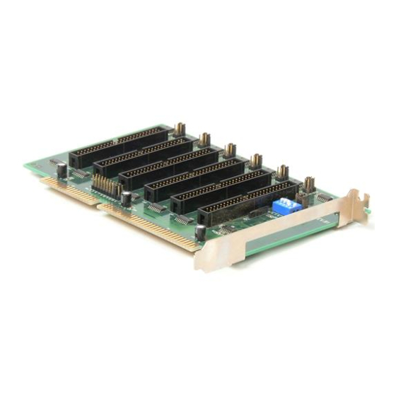
Page 16: Acl-7122'S Layout
2.3 ACL-7122's Layout Figure 2.1 Installation • 7... -
Page 17: Jumper And Dip Switch Description
2.5 DIO Channel No. Setting The ACL-7122 can provide two kinds of I/O capability modes 144-bit and 96-bit, which are selected by DIP switch JP7 (see Figure 2.2 below). The 144-bit mode requires 32 consecutive I/O address ports, and 96-bit mode just occupies 16 address ports. -
Page 18: Base Address Setting
2.6 Base Address Setting The ACL-7122 requires 32 or 16 consecutive address locations in I/O address space. The base address of the ACL-7122 is restricted by the following conditions. 1. The base address must be within the range 200hex to 3FFhex. - Page 19 I/O port address(hex) 200-21F (*) 2C0-2DF 380-29F 3A0-3BF 3C0-3DF 3E0-3FF (*) : default setting X : Don't care ON = 0 ; OFF = 1 A2, ..., A8 are corresponding to address lines of ISA bus. A9 is always 1 (OFF). Table 2.2 144-bit mode Note : In 144-bit mode, the base address line A4 is not in functional status, so, do not care the position of A4 of SW1.
-
Page 20: Interrupt Setting
Base Address : Hex 2C0 2.7 Interrupt Setting The ACL-7122 provides 11 interrupt requests IRQ 3, 4, 5, 6, 7, 9, 10, 11, 12, 14, and 15, which could be set for hardware interrupt generated by pins PC-0 and PC-3 of each channel. The IRQ is set by jumper JP6.(Ref. - Page 21 The ACL-7122 has two lines (PC-0 and PC-3) for each channel to generate hardware interrupt. The interrupt are edge-triggered, PC-0 traps a rising edge signal, which PC-3 traps a falling edge signal. To use the interrupt, first you have to select the desired IRQ interrupt level.
- Page 22 JPn( n=0...5) PC0 Interrupt Status No Interrupt Request L -> H LOW Interrupt Request L->H HIGH HIGH LOW No Interrupt Request HIGH No Interrupt Request HIGH Interrupt Request Interrupt Request X : Don't Care H-> L : Rising Edge Trigger ( from High to Low) L->H : Falling Edge Trigger ( from Low to High) Installation •...
-
Page 23: Connector Pin Assignment
2.8 Connector Pin Assignment The I/O ports of ACL-7122 emulates as six mode 0 Intel 8255 general purpose programmable peripheral interface. Figure 2.4 shows ACL-7122's equally block diagram. There are six 50-pin connectors come equipped with the ACL-7122 board, and each of them is corresponding to a mode 0 of 8255. - Page 24 Port C D7 Port C D6 Port C D5 Port C D4 Port C D3 Port C D2 Port C D1 Port C D0 Port B D7 Port B D6 Port B D5 Port B D4 Port B D3 Port B D2 Port B D1 Port B D0 Port A D7...
-
Page 25: Connection
2.9 Connection There are three daughter boards to connect with ACL-7122 for DIO operation. The following diagrams show you how to configuration your ACL-7122 with different terminal boards. 1. TB-24R The TB-24R provides 24 Form C relays for digital output control. -
Page 26: Chapter 3 Digital I/O Programming
Digital I/O Programming 3.1 Register Structure & Format The ACL-7122 needs 24 bytes of I/O address to operate. The relationship of I/O address and ports' data read / write shows as following table (Table 4.2), the default base address of below table is 2C0H. -
Page 27: Mode 0 Of 8255 Ppi
Table 4.2 Ports' I/O address table (Base Address = 2C0H) 3.2 Mode 0 of 8255 PPI The ACL-7122 can emulates MODE 0 of 8255 PPI, and it comes equipped with six 50-pin male IDC connectors that interface with OPTO-22 racks 8, 16, and 24. -
Page 28: Interrupt Handling
Table 4.1 Summarize of control word (D0 - D4) and mode state (Mode 0 - Mode 15) 3.3 Interrupt Handling The ACL-7122 can generate a hardware interrupt to your PC. The following issues should be careful when you want to generate an interrupt trigger. -
Page 29: Programming Notes
Interrupt Request No Interrupt Request High (X) : Don't care Note : Since the ACL-7122's Input is not latched and no first event trapping is provided to determine which input was active first. Self Interrupt Trigger Although the ACL-7122's interrupt signals are normal received from external peripherals. - Page 30 Buffer READ Figure 3.1 ACL-7122's Signal Direction 3. According the above ACL-7122's signal direction block diagram, some issues should be careful. a. When a port is set as INPUT or after hardware RESET, its output buffer is Disabled (high impedance) b.
-
Page 31: Programming In C Language
3.5 Programming in C language The following parts are example programs written in C language. The first four parts are just partial programs for your reference, you can not compile them before these programs are complete. The last program is an example for interrupt handling, you could compile it by Borland C/C++ compiler directly. - Page 32 5. A Complete Example Program for Interrupt Handling /****************************************************/ This program deno. how to generate interrupt by * the ACL-7122 itself. When you press any key, a beep is generated. When you press ESC key, the system will be quit.
- Page 33 #define IRQ2 0x0a #define 0x20 #define BASE_ADDR 0x2c0 #define 0x00 #define 0x01 #define 0x02 #define 0x03 void interrupt isr_7122() printf("\7"); // beep outportb( 0x20, EOI); // EOI of 8259 main() mask, keyin; void interrupt (*old_irq2_isr)(); old_irq2_isr = getvect( IRQ2); setvect( IRQ2, isr_7122); mask = inportb( 0x21);...
-
Page 34: Appendix A. I/O Port Address Map
Appendix A. I/O Port Address Map I/O Address Device 000-01F DMA controller 1 020-03F interrupt controller 040-05F Timer 060-06F Keyboard 070-07F Real-time clock 080-09F DMA page register 0A0-0BF Interrupt controller 2 0C0-0DF DMA controller 0F0-0FF Math coprocessor 100-1EF not usable 1F0-1F8 Fixed disk 200-207... -
Page 36: Product Warranty/Service
Product Warranty/Service Seller warrants that equipment furnished will be free form defects in material and workmanship for a period of one year from the confirmed date of purchase of the original buyer and that upon written notice of any such defect, Seller will, at its option, repair or replace the defective item under the terms of this warranty, subject to the provisions and specific exclusions listed herein.
Need help?
Do you have a question about the ACL-7122 and is the answer not in the manual?
Questions and answers