Table of Contents
Advertisement
Quick Links
Advertisement
Table of Contents

Related Manuals for ADLINK Technology PCI-725 Series


Summary of Contents for ADLINK Technology PCI-725 Series
- Page 1 PCI-/cPCI-/LPCI-/ LPCIe-725X Series 8-CH Relay Output & 8-CH Isolated Digital Input Cards User’s Manual Manual Rev. 2.03 Revision Date: June 24, 2008 Part No: 50-11038-1000 Advance Technologies; Automate the World. This datasheet has been downloaded from http://www.digchip.com at this page...
- Page 2 Copyright 2008 ADLINK TECHNOLOGY INC. All Rights Reserved. The information in this document is subject to change without prior notice in order to improve reliability, design, and function and does not represent a commitment on the part of the manufacturer.
- Page 3 Getting Service from ADLINK Customer Satisfaction is top priority for ADLINK Technology Inc. Please contact us should you require any service or assistance. ADLINK TECHNOLOGY INC. Web Site: http://www.adlinktech.com Sales & Service: Service@adlinktech.com TEL: +886-2-82265877 FAX: +886-2-82265717 Address: 9F, No. 166, Jian Yi Road, Chungho City,...
-
Page 5: Table Of Contents
Table of Contents Table of Contents..............i List of Tables................iii List of Figures ................ iv 1 Introduction ................ 1 Features................2 Applications ................. 2 Specifications............... 3 Digital input ..............3 Relay Output ..............3 General Specifications ............ 4 Power Consumption ............4 Software Support .............. - Page 6 LPCI/LPCIe-7250 CN1 Pin Assignment ....... 27 PCI-7250 and PCI-7251 Connection ......... 28 3 Registers................29 PCI PnP Registers ............. 29 I/O Address Map ..............30 Relay Output and Readback Registers......30 Isolation Input Registers ............ 31 4 Operation Theory .............. 33 Using Relay Output............
-
Page 7: List Of Tables
List of Tables Table 1-1: Digital Input Specifications ........3 Table 1-2: Relay Output Specifications ........3 Table 1-3: General Specifications ..........4 Table 1-4: Power Consumption Specifications ......4 Table 2-1: Jumpers and DI Channels ........22 Table 2-2: Input Signal Selection Jumper Settings ....22 Table 2-3: CN1 - PCI-7250/51 Pin Assignment ....... - Page 8 List of Figures Figure 2-1: PCI-7250 Layout............18 Figure 2-2: cPCI-7252 Layout ............ 19 Figure 2-3: LPCI-7250 PCB Layout ........... 20 Figure 2-4: LPCIe-7250 PCB Layout ......... 21 Figure 2-5: CN1 - D Type Connector ......... 24 Figure 2-6: Connection between PCI-7250 and PCI-7251..28 Figure 4-1: Form C Relay............
-
Page 9: Introduction
Introduction The PCI-7250/7251, cPCI-7252, LPCI-7250 and LPCIe-7250 8- CH Relay Output & 8-CH Isolated Digital Input Cards are basic Digital I/O cards for PCI bus compliant computers used in indus- trial applications. This PCI-7250/7251 provide 8 relay actuators and 8 opto-isolated digital inputs. -
Page 10: Features
1.1 Features The PCI-725X Relay Actuator and D/I cards provide the following advanced features: 32-bit PCI-Bus, Plug and Play (PCI-7250, LPCI-7250) ® 32-bit CompactPCI Bus, Plug and Play (cPCI-7252) 8 relay actuator outputs 8 opto-isolated digital inputs (PCI-7250, LPCI-7250, LPCIe-7250) x1 lane PCI Express Interface (LPCIe-7250) 16 opto-isolated digital inputs (cPCI-7252) Onboard LED indicators to show energized relays... -
Page 11: Specifications
1.3 Specifications Digital input 8 for PCI-7250, PCI-7251, LPCI-7250 and LPCIe-7250 Input channels 16 for cPCI-7252 PC-814 (for PCI-7250, PCI-7251 and cPCI-7252) Photo-coupler PC3H4 (for LPCI-7250 and LPCIe-7250) 10 mA rated Input current 60 mA max for isolated input Up-to 24 VDC or 24 VAC 50-1,000 Hz Input Voltage Logic Low: 0-1.5 V Logic High 5-24 V... -
Page 12: General Specifications
PCI-7250/7251, cPCI-7252: >5x10 operations @ 1 A, 24 VDC >2x10 operations @ 0.5 A, 120 VAC Life expectancy LPCI-7250/LPCIe-7250: >10 operations @ 2 A, 30 VDC >5x10 operations @ 1 A, 30 VDC LED indicators Monitor ON/OFF status of each relay Coil Voltage +5V, 33 mA for each relay, total 0.264 A +5 V from the PCI-Bus (PCI-7250/7251, cPCI-7252, LPCI-7250) -
Page 13: Software Support
1.4 Software Support ADLINK Technology Inc., a leading provider of high-performance, high-quality data acquisition cards and platforms, delivers robust software support for its comprehensive line of DAQ cards with varying form factors including PCI Express®, PCI, CompactPCI, and PXI. ADLINK offers support not only for mainstream Windows and Linux OS, but also for third-party applications including Lab- VIEW®... -
Page 14: Windows Drivers
Windows Drivers ADLINK Task-oriented DAQ Driver/SDK and Wizard for Win- dows DAQPilot provides one interface for all ADLINK DAQ products via DAQPilot API DAQPilot ActiveX Control DAQPilot .Net Assembly, DAQPilot (Download and install from the DAQPilot product page: http://www.adlinktech.com/TM/DAQPilot.html Save development time Shorten learning curve DAQPilot is a driver and SDK with a graphics-driven interface for various ADE. - Page 15 immediately program ADLINK DAQ modules and integrate tasks to their own DAQ applications. Note: ADLINK strongly recommend all users to install the new- generation ADLINK Driver – DAQPilot instead legacy DASK drivers. For those users who have been using the legacy ADLINK DASK Drivers or are not able to connect to the in- ternet, you still can get the latest update from ADLINK all-in- one CD.
- Page 16 Configuration-Based Device Manager for ADLINK DAQ Cards DAQMaster (.\Utility) The ADLINK DAQMaster is a smart device manager that enables access to ADLINK data acquisition and test and measurement products. DAQMaster delivers an all-in-one configurations, user can get a full support matrix to well configure ADLINK Test and Measurement products.
- Page 17 ADLINK Legacy DAQ Card Drivers and SDK for Windows PCIS-DASK (.\Software Package\PCIS-DASK) D2K-DASK (.\Software Package\D2K-DASK) WD-DASK (.\Software Package\WD-DASK) User Mode Kernel Mode Delphi Process Structure DASK Kernel Driver PCIS-DASK (.sys) Object Manager VC++ Memory Executive D2K-DASK Manager Support Configuration Power Plug and Pay Manager Manager...
- Page 18 More information about Windows Vista Support, please visit http:// www.adlinktech.com/TM/VistaSupport.html. Note: Please use PCIS-DASK with the LPCI-7250 and LPCIe- 7250 Introduction...
-
Page 19: Linux Drivers
Linux Drivers Linux Drivers for ADLINK DAQ Cards Drivers are available on the ADLINK website: PCIS-DASK/X D2K-DASK/X WD-DASK/X ADLINK's DASK/X drivers are intended for developing customized data acquisition applications under Linux environments. The DASK/X drivers provide common APIs for ADLINK's extensive family of PCI, CompactPCI, and PXI plug-in data acquisition cards, and utilize the full capabilities of these cards under Linux environment. -
Page 20: Third-Party Software Support
Third-party Software Support MATLAB® Data Acquisition Toolbox Adapter for ADLINK DAQ Cards DAQ-MTLB for MATLAB® (.\Software Package\DAQ- MTLB) The DAQ-MTLB for MATLAB® integrates ADLINK components with MATLAB® Data Acquisition Toolbox and enables users to control a wide range of ADLINK DAQ cards directly from the advanced MATLAB®... - Page 21 LabVIEW™ Data Acquisition VI Set for ADLINK DAQ Cards DAQ Cards DAQ-LVIEW PnP for LabVIEW™ (.\Software Package\DAQ-LVIEW PnP) The DAQ-LVIEW PnP is a set of LabView Virtual Instruments (Vis) that is fully-compatible with National Instrument's DAQ VIs. Based on the virtual instruments concept, DAQ-LVIEW PnP provides four additional tool panels in LabView, including analog input, analog output, digital I/O, and timer/counter.
-
Page 22: Vee™ Interface For Adlink Daq Cards
VEE™ Interface for ADLINK DAQ Cards PCIS-VEE (.\Software Package\PCIS-VEE) D2K-VEE (.\Software Package\D2K-VEE) Agilent VEE™ is a popular visual programming environment for data acquisition that includes data analysis and control. VEE pro- vides a visual programming interface that allows users to create programs by connecting objects such as acquisition routines, but- tons and displays in a flow diagram. -
Page 23: Componentware/Activex Control
Componentware/ActiveX Control 32-Bit ActiveX Controls for Measurement and SCADA/HMI DAQBench (.\Software Package\DAQBench) DAQBench is a specialized ActiveX control package designed for 32-bit measurement and SCADA/HMI applications. DAQBench leverages the power of the latest Microsoft ActiveX technology - the standard for code interchangeability and integration under var- ious Windows platform. -
Page 24: Applications For Test And Measurement
Applications for Test and Measurement Smart & Easy-to-Use Data Acquisition System Creator DAQCreator (.\Software Package\DAQCreator) DAQCreator is an out-of-the-box data acquisition software for acquiring, displaying, analyzing, and storing data from ADLINK DAQ cards. Equipped with a smart wizard and intuitive panels, users can easily configure data acquisition settings, change the appearance of data display, perform FFT to acquired data, and store data to a hard disk drive. -
Page 25: Installation
Installation This chapter describes how to install and setup the 725X cards. Jumper settings for the digital input channel configurations (AC-fil- ter or Non-AC-filter) and the signal definitions of the 37-pins con- nectors are also specified. 2.1 Unpacking Checklist Check the shipping carton for any damage. If the shipping carton and contents are damaged, notify the dealer for a replacement. -
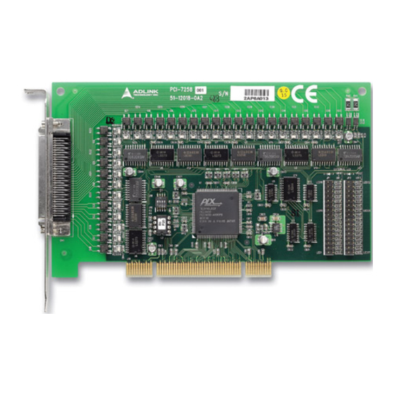
Page 26: Pcb Layout
2.2 PCB Layout PCI-7250 PCB Layout Figure 2-1: PCI-7250 Layout Installation... -
Page 27: Cpci-7252 Pcb Layout
cPCI-7252 PCB Layout Figure 2-2: cPCI-7252 Layout Installation... -
Page 28: Lpci-7250 Pcb Layout
LPCI-7250 PCB Layout Figure 2-3: LPCI-7250 PCB Layout Installation... -
Page 29: Lpcie-7250 Pcb Layout
LPCIe-7250 PCB Layout Figure 2-4: LPCIe-7250 PCB Layout Installation... -
Page 30: Input Signal Jumper Setting
2.3 Input Signal Jumper Setting Note: This section is for PCI-7250, PCI-7251, LPCI-7250, and LPCIe-7250 only. There are 8 jumpers (JP1 to JP8) on the PCI-7250, PCI-7251, LPCI-7250 and LPCIe-7250; each associated with one digital input to configure that channel as either AC-Filtered or Non-AC- Filtered. -
Page 31: Hardware Installation Outline
2.4 Hardware Installation Outline PCI Configuration PCI cards (or CompactPCI cards) are equipped with plug and play PCI controllers which can request base addresses and interrupts according to the PCI standard. The system BIOS will assign the system resources based on the PCI card configuration registers and system parameters (which are set by the system BIOS). -
Page 32: Device Installation For Windows Systems
2.5 Device Installation for Windows Systems Once Windows Vista/XP/2003/2000 has started, the Plug and Play functions of the Windows system will find and locate the new NuDAQ/NuIPC card. If this is the first time a NuDAQ/NuIPC card is installed in your Windows system, you will be prompted to input the device information source. -
Page 33: Table 2-3: Cn1 - Pci-7250/51 Pin Assignment
Legend Digital input low, channel n Din: (input signal Is not polarity sensitive) NC n: Normal close pin of relay n NO n: Normal open pin of relay n COM n: Common pin of relay n N/C: No connection Table 2-3: CN1 - PCI-7250/51 Pin Assignment Installation... -
Page 34: Cpci-7252 Pin Assignment
cPCI-7252 Pin Assignment Signal Pin Pin Signal IGND IGND DI12 DI13 DI10 DI14 DI11 DI15 DI0L DI4H DI0H DI4L DI1L DI5H DI1H DI5L D2IL DI6H DI2H DI6L DI3L DI7H DI3H DI7L COM0 COM5 COM1 COM4 COM2 COM7 COM3 COM6 Table 2-4: CN1 - cPCI-7252 Pin Assignment Legend Din: Digital input channel n... -
Page 35: Lpci/Lpcie-7250 Cn1 Pin Assignment
LPCI/LPCIe-7250 CN1 Pin Assignment Signal Pin Pin Signal COM0 COM4 COM1 COM5 COM2 COM6 COM3 COM7 IDI_0H IDI_0L IDI_1H IDI_1L IDI_2H IDI_2L IDI_3H IDI_3L IDI_4H IDI_4L IDI_5H IDI_5L IDI_6H IDI_6L IDI_7H IDI_7L Table 2-5: LPCI/LPCIe-7250 CN1 Pin Assignment Legend Din: Digital input channel n IGND: Ground of DIn signals... -
Page 36: Pci-7250 And Pci-7251 Connection
2.7 PCI-7250 and PCI-7251 Connection There are 8-relay outputs and 8-isolation inputs on both the PCI- 7250 and PCI-7251. The PCI-7251 is used as an expansion for the PCI-7250. The operations of the PCI-7251 are the same as that of the PCI-7250. There can be at most 3 PCI-7251 expansion boards to one PCI-7250. -
Page 37: Registers
Registers Detailed descriptions of the registers are specified in this chapter. This information is useful for programmers who wish to control the card with low-level programming. However, we suggest users fully understand the PCI interface before starting any low-level pro- gramming. -
Page 38: I/O Address Map
3.2 I/O Address Map All 725X registers are 8 bits long. Users can access these regis- ters using 8-bit I/O instructions. Using these registers will allow the relays and status of the inputs to be controlled. The following table shows the registers address map, including descriptions and their offset addresses relative to the base address. -
Page 39: Isolation Input Registers
The normal open signal line is ‘open’. Bit value ‘1’ means the relay is energized and the normal open signal line is now closed. The initial bit values of the control register are all ‘0’ and the status of the relay can be readback from the readback register. If the relay is open, the corresponding bit value read is ‘0’. - Page 40 Registers...
-
Page 41: Operation Theory
Operation Theory 4.1 Using Relay Output The PCI-7250/7251 contains two types of relays: Form C and Form A. Relays R0 - R3 are form C relays, and R4 - R7 are plain form A type. Note that the LPCI-7250, LPCIe-7250, and cPCI- 7252 contain Form C relays only. -
Page 42: Figure 4-2: Form A Relay
2. Form A Relay: (R4 - R7) Control Bit = High(1) Control Bit = Low(0) Figure 4-2: Form A Relay Form A relay only has two contacts: NO (Normal Open) and COM (Common). The COM post can make contact either with the NO post or not. -
Page 43: Using Isolated Input
4.2 Using Isolated Input The PCI-7250 (or PCI-7251) contains 8 identical opto-isolated control input channels. The circuit diagram of the differential input channel is shown below. Ω 2.2k DInH DInL PC-814 (opto-isolator) Figure 4-3: PCI-7250 Differential Input Circuit The digital input is first routed through a photo-coupler (PC-814), which is shown in the following diagram. -
Page 44: Figure 4-5: Lpci/Lpcie-7250 Differential Input Circuit
The LPCI-7250 and LPCIe-7250 contain 8 identical opto-isolated control input channels through PC3H4 photo-coupler. The circuit is shown as the following diagram: Ω 2.2k DInH DInL PC3H4 (opto-isolator) Figure 4-5: LPCI/LPCIe-7250 Differential Input Circuit In addition, a single-pole filter with a time constant of about 5ms is used to filter AC inputs passing through. -
Page 45: Appendix
Appendix Relay Contact Protection Circuits The contacts are the most important elements of a relay construc- tion, Contact performance conspicuously influenced by contact material, and voltage and current values applied to the contacts. Another important issue is contact protection; the right contact pro- tection circuit can suppress the counter EMF to a low level. -
Page 46: Diode Circuit
Device Selection: As a guide in selecting R and C, Ω R: 0.5 to 1 per 1V contact voltage μ C: 0.5 to 1 F per 1A contact current Values vary depending on the properties of the capacitor C acting to suppress the discharge the moment the contacts open. -
Page 47: Diode & Zener Diode Circuit
Diode & Zener diode Circuit This circuit is also suitable for DC application. Effective when the release time i in the diode circuit is too long. Contact Diode Inductive Load Device Selection: Use a zener diode with a zener voltage about the same as the power supply voltage. - Page 48 Appendix...
Need help?
Do you have a question about the PCI-725 Series and is the answer not in the manual?
Questions and answers