
Related Manuals for ADLINK Technology PCIe-7396


Summary of Contents for ADLINK Technology PCIe-7396
- Page 1 PCIe-7396 96-Channel Digital I/O Card User’s Manual Manual Rev.: February 2, 2021 Revision Date: 50-15117-1000 Part No: Leading EDGE COMPUTING...
- Page 2 Leading EDGE COMPUTING Revision History Revision Release Date Description of Change(s) 2021-02-02 Initial release.
- Page 3 PCIe-7396 Preface Copyright © 2021 ADLINK Technology Inc. This document contains proprietary information protected by copy- right. All rights are reserved. No part of this manual may be repro- duced by any mechanical, electronic, or other means in any form without prior written permission of the manufacturer.
- Page 4 Leading EDGE COMPUTING California Proposition 65 Warning WARNING: This product can expose you to chemicals including acrylamide, arsenic, benzene, cadmium, Tris(1,3-dichloro-2-propyl) phosphate (TDCPP), 1,4- Dioxane, formaldehyde, lead, DEHP, styrene, DINP, BBP, PVC, and vinyl materials, which are known to the State of California to cause cancer, and acrylamide, benzene, cadmium, lead, mercury, phthalates, toluene, DEHP, DIDP, DnHP, DBP, BBP, PVC, and vinyl materials, which are known to the State of California to cause...
-
Page 5: Table Of Contents
PCIe-7396 Table of Contents Preface ..................iii List of Tables................. vii List of Figures ................ ix 1 Introduction ................ 1 Features................1 Applications ................. 2 Specifications............... 2 Software Support ..............3 2 Getting Started ..............5 Package Contents ............... 5 Unpacking................ - Page 6 Leading EDGE COMPUTING 8254 Timer/Counter Operation .......... 22 Interrupt Circuit ..............23 Important Safety Instructions..........29 Consignes de Sécurité Importante ........31 Getting Service ..............35 Table of Contents...
-
Page 7: List Of Tables
PCIe-7396 List of Tables Table 2-1: Board Features Legend..........6 Table 2-2: SCSI Connector Pin Assingments......9 Table 2-3: Jumpers and Port Names......... 10 Table 3-1: Register Map ............14 Table 4-1: ISC Register Format..........25 Table 4-2: IRQ Trigger Conditions..........26... - Page 8 Leading EDGE COMPUTING This page intentionally left blank. viii List of Tables...
-
Page 9: List Of Figures
PCIe-7396 List of Figures Figure 2-1: Board Layout ..............6 Figure 2-2: SCSI Connector............... 8 Figure 4-1: External Trigger Function Block Diagram ...... 21 Figure 4-2: Read Data Using External Trigger Diagram ....21 Figure 4-3: Timer/Counter System Block Diagram ......22 Figure 4-4: Dual Interrupt System ............ - Page 10 Leading EDGE COMPUTING This page intentionally left blank. List of Figures...
-
Page 11: Introduction
PCIe-7396 Introduction The PCIe-7396 is a 96-bit parallel digital input/output (DIO) card designed for industrial applications. The plug and play feature of PCI Express Bus architecture makes it easy for users to install the PCIe-7396 on their systems quickly. The PCIe-7396 emulates two/four 8255 Programmable Peripheral Interface (PPI) chips. -
Page 12: Applications
Leading EDGE COMPUTING 1.2 Applications Programmable mixed digital input and output Industrial monitoring and control LED indicator control Parallel data transfer TTL, DTL, and CMOS logic sensing 1.3 Specifications Item Specification I/O channels 96-bit Logic High Voltage: 2.0V to 5.25V Logic Low Voltage: 0.0V to 0.08V Input Signal Logic High Current: 0.1 μA... -
Page 13: Software Support
PCIe-7396 1.4 Software Support ADLINK provides versatile software drivers and packages to suit various user approaches to building a system. Aside from pro- gramming libraries, such as DLLs, for most Windows-based sys- tems, ADLINK also provides drivers for other application environments such as LabVIEW. - Page 14 Leading EDGE COMPUTING 1.4.2 ADLINK MAPS/LV, LabVIEW Support For customers who develop their own programs in LabVIEW, the MAPS/LV software package must be installed. MAPS/LV, also called DAQ-LabVIEW Plus, includes the software library and sam- ple program for LabVIEW. Download and install the latest MAPS/ LV software and refer to the MAPS/LV manual for more informa- tion.
-
Page 15: Getting Started
Inspect the card module carton for obvious damage, as shipping and handling may cause damage to the module. Be sure the mod- ule is not damaged before proceeding. Do not apply power to the PCIE-7396 if it has been damaged. CAUTION: Getting Started... -
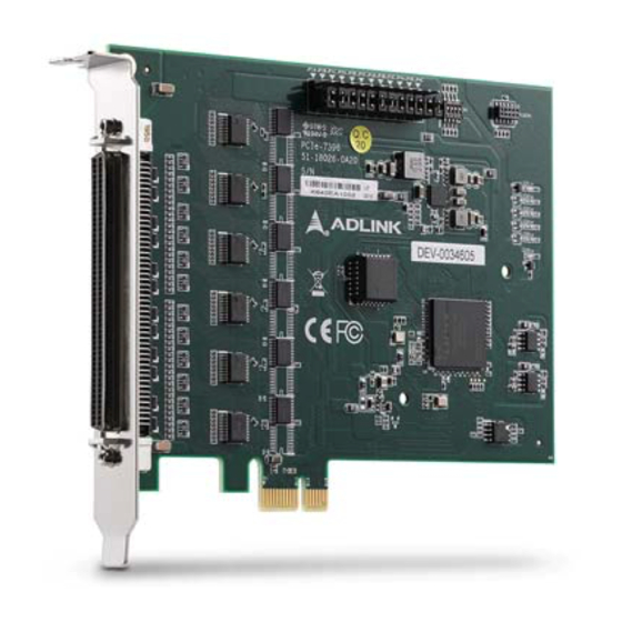
Page 16: Board Layout
Leading EDGE COMPUTING 2.3 Board Layout Figure 2-1: Board Layout Item Description Power-On State Selection Jumper Card ID Selection Switch (Reserved) Table 2-1: Board Features Legend Getting Started... -
Page 17: Installation
It is not sug- gested to assign the system resource by any other method. 2.4.2 PCI Express Slot Selection The PCIe-7396 can be inserted into any PCI Express slot without the need to configure system resources. 2.4.3 Installation Procedures 1. -
Page 18: Scsi Connector
Leading EDGE COMPUTING 2.5 SCSI Connector (51) (50) (100) Figure 2-2: SCSI Connector Getting Started... -
Page 19: Table 2-2: Scsi Connector Pin Assingments
PCIe-7396 Signal Signal Signal Signal P3A0/ P1A0 (26) P2A0 (51) (76) P4A0 EVENT P1A1 (27) P2A1 (52) P3A1 (77) P4A1 P1A2 (28) P2A2 (53) P3A2 (78) P4A2 P1A3 (29) P2A3 (54) P3A3 (79) P4A3 P1A4 (30) P2A4 (55) P3A4 (80) -
Page 20: Jumpers
GND: Ground 2.6 Jumpers The PCIe-7396 is a ‘plug and play’ add-on card using the PCI Express bus. It is unnecessary to set up its base address and IRQ level to fit the hardware of the computer system. However, there are some jumpers to set the power-on-states of all I/O ports. -
Page 21: Terminal Board Support
Port A of PPI1 is pulled high. When the jumper cap is removed, the power-on-state is floating. 2.7 Terminal Board Support The PCIe-7396 can be connected to several different daughter boards, including the DIN-100S, DIN-96DI, and DIN-96DO (EOL). The functionality and connections are specified as follows. - Page 22 Leading EDGE COMPUTING 2.7.3 DIN-96DO Terminal Board (EOL) The DIN-96DO digital output termination board features high-volt- age opto-isolation on all outputs to prevent floating potential and ground loop problems from damaging the system. It is composed of one TB-96 baseboard, one TB-96DO daughter board, and one DIN socket for easy maintenance, wiring, and installation.
-
Page 23: Register Format
PCIe-7396. 3.1 I/O Address Map Most of the PCIe-7396 registers are 32 bits. Users can access these registers with 32-bit I/O instructions. The following table shows the register map, including descriptions and their offset addresses relative to the base address. -
Page 24: Table 3-1: Register Map
Leading EDGE COMPUTING Offset Write Read 0x00 P1ABC P1ABC 0x04 P1Control Not used 0x08 P1EXTTRG Enable Not used 0x0C P1EXTTRG Disable Not used 0x10 P2ABC P2ABC 0x14 P2Control Not used 0x18 P2EXTTRG Enable Not used 0x1C P2EXTTRG Disable Not used 0x20 P3ABC P3ABC... -
Page 25: Ppi Registers
COS Interrupt Control Register, detailed in the following sections. 3.2.1 Digital Data Register The 24-bit I/O data of the PCIe-7396 is accessed from/to this reg- ister by software. The digital data can also be read back through this register. Address: BASE + 00h... - Page 26 Leading EDGE COMPUTING 3.2.2 Control Register Each PPI’s control register is used to set its three ports to be as input or output independently. Address: BASE + 04h Attribute: write only Data Format: BASE+04h BASE+05h BASE+06h BASE+07h P1n: n: port number Set to ‘0’...
- Page 27 PCIe-7396 3.2.4 External Trigger Disable Register Users can write anything to this register to disable the function of external trigger. Address: BASE + 0Ch Attribute: write only Data Format: BASE+0Ch BASE+0Dh BASE+0Eh BASE+0Fh 3.2.5 Change of State (COS) Interrupt Control Register This register is used to configure the COS interrupt.
-
Page 28: Interrupt Source Control (Isc) Register
Leading EDGE COMPUTING 3.3 Interrupt Source Control (ISC) Register The PCIe-7396 has a dual interrupt system. Two interrupt sources can be generated and be distinguished by software settings. This register is used to select the interrupt sources. Address: BASE + 50h... -
Page 29: Clear Interrupt Register
BASE+55h BASE+56h BASE+57h 3.5 Timer/Counter Register The 8254 chip occupies 4 I/O addresses in the PCIe-7396. Refer to NEC's or Intel's datasheet for the full description of the 8254’s operations. Address: BASE + 40h to BASE + 4Ch Attribute: read/write... -
Page 30: High Level Programming
Leading EDGE COMPUTING 3.6 High Level Programming You can bypass the detailed register structures of the PCIe-7396 with a high-level application programming interface (API). Register Format... -
Page 31: Functional Operations
PCIe-7396. 4.1 Digital I/O Ports The PCIe-7396 has 2/4 onboard PPIs. Each 24-bit PPI is divided into three 8-bit I/O ports: A, B, and C. All of these 6/12 ports can be programmed as input or output independently. -
Page 32: 8254 Timer/Counter Operation
Leading EDGE COMPUTING 4.2 8254 Timer/Counter Operation One 8254 programmable timer/counter chip is installed on the PCIe-7396. There are three counters and six possible operation modes for each counter. 8254 Chip EVENT Event Edge Event IRQ (PIN 51) Control Counter #0... -
Page 33: Interrupt Circuit
4.3.2 IRQ Level Setting There is only one IRQ level needed in the PCIe-7396, although it is a dual interrupt system, because it uses INT #A interrupt request signal on the PCI Express bus. The motherboard circuits transfer INT #A to one of the AT bus IRQ levels. The IRQ level is set by the BIOS and saved in the PCI Express controller. -
Page 34: Figure 4-4: Dual Interrupt System
Leading EDGE COMPUTING 4.3.3 Dual Interrupt System The PCI Express controller can receive two hardware IRQ requests. However, only one IRQ will be sent to the PCI Express bus, the two IRQ requests must be distinguished by an interrupt service routine (ISR). The two IRQ requests are INT1 and INT2. -
Page 35: Table 4-1: Isc Register Format
PCI Express controller. INT1 IRQ Sources IRQ Trigger Condition Disable INT1 disable Mode 1 COS P1&P2 (48 bits) Change of State for PCIe-7396 (default) Mode 2 P1C0 OR -P1C3 (see Table 4-2 on page 26) Mode 3 -P1C0... -
Page 36: Table 4-2: Irq Trigger Conditions
Leading EDGE COMPUTING When the IRQ sources is set as “P1C0 OR -P1C3” or “P2C0 OR - P2C3”, the IRQ trigger conditions are summarized in Table 4-2. P1C0 P1C3 IRQ Trigger Condition High P1C0=‘H’ disable all IRQ P1C3=‘L’ disable all IRQ 1->0 P1C3 falling edge trigger when P1C0=L 0->1... -
Page 37: Figure 4-5: Change Of State (Cos) Interrupt
A Change of State (COS) occurs when the input state (logic level) is changed from low to high, or from high to low. The COS detec- tion circuit will detect the edge of level change. On the PCIe-7396, the COS detection circuit is applied to all the input channels. When any channel changes its logic level, the COS detection circuit gen- erates an interrupt request to the PCI Express controller. - Page 38 Leading EDGE COMPUTING This page intentionally left blank. Functional Operations...
-
Page 39: Important Safety Instructions
PCIe-7396 Important Safety Instructions For user safety, please read and follow all instructions, Warnings, Cautions, and Notes marked in this manual and on the associated device before handling/operating the device, to avoid injury or damage. Read these safety instructions carefully. - Page 40 Leading EDGE COMPUTING A Lithium-type battery may be provided for uninterrupted backup or emergency power. Risk of explosion if battery is replaced with one of an incorrect type; please dispose of used batteries appropriately. CAUTION: This equipment is not suitable for use in locations where children are likely to be present.
-
Page 41: Consignes De Sécurité Importante
PCIe-7396 Consignes de Sécurité Importante S'il vous plaît prêter attention stricte à tous les avertissements et mises en garde figurant sur l'appareil, pour éviter des blessures ou des dommages. Lisez attentivement ces consignes de sécurité. Conservez le manuel de l'utilisateur pour pouvoir le con- sulter ultérieurement. - Page 42 Leading EDGE COMPUTING Si l'appareil ne doit pas être utilisé pendant de longues péri- odes, éteignez-le et débranchez-le de sa source d'alimenta- tion N'essayez jamais de réparer l'appareil, qui ne doit être réparé que par un personnel technique qualifié à l'aide d'outils appro- priés Une batterie de type Lithium peut être fournie pour une ali- mentation de secours ininterrompue ou d'urgence.
- Page 43 PCIe-7396 RISQUE DE BRÛLURES Partie chaude! Ne touchez pas cette surface, cela pourrait entraîner des blessures. Pour éviter tout danger, laissez la surface refroidir avant de la toucher. Consignes de Sécurité Importante...
- Page 44 Leading EDGE COMPUTING This page intentionally left blank. Consignes de Sécurité Importante...
-
Page 45: Getting Service
San Jose, CA 95138, USA Tel: +1-408-360-0200 Toll Free: +1-800-966-5200 (USA only) Fax: +1-408-360-0222 Email: info@adlinktech.com ADLINK Technology (China) Co., Ltd. 300 Fang Chun Rd., Zhangjiang Hi-Tech Park Pudong New Area, Shanghai, 201203 China Tel: +86-21-5132-8988 Fax: +86-21-5132-3588 Email: market@adlinktech.com ADLINK Technology GmbH Hans-Thoma-Straße 11...
Need help?
Do you have a question about the PCIe-7396 and is the answer not in the manual?
Questions and answers