
Related Manuals for ADLINK Technology PCIe-7300A


Summary of Contents for ADLINK Technology PCIe-7300A
- Page 1 PCI/PCIe/cPCI-7300A 80 MB Ultra-High Speed 32-CH Digital I/O Boards User’s Manual Manual Rev. 2.50 Revision Date: July 1, 2008 Part No: 50-11106-1030 Advance Technologies; Automate the World.
- Page 2 Copyright 2008 ADLINK TECHNOLOGY INC. All Rights Reserved. The information in this document is subject to change without prior notice in order to improve reliability, design, and function and does not represent a commitment on the part of the manufacturer.
- Page 3 Getting Service from ADLINK Customer Satisfaction is top priority for ADLINK Technology Inc. Please contact us should you require any service or assistance. ADLINK TECHNOLOGY INC. Web Site: http://www.adlinktech.com Sales & Service: Service@adlinktech.com TEL: +886-2-82265877 FAX: +886-2-82265717 Address: 9F, No. 166, Jian Yi Road, Chungho City,...
-
Page 5: Table Of Contents
DAQBenchTM: ActiveX Controls ........7 2 Installation ................9 What You Have..............9 Unpacking................10 Device Installation for Windows Systems ......10 cPCI/PCI/PCIe-7300A Layout..........11 Hardware Installation Outline..........13 Connector Pin Assignment ..........14 Wiring and Termination............. 17 Termination Board Support..........18 Connect with DIN-100S .......... - Page 6 4 Operation Theory .............. 33 I/O Configuration..............34 Block Diagram..............35 Digital I/O Data Flow ............36 Input FIFO and Output FIFO..........37 Bus-mastering DMA............38 Scatter/gather DMA ............40 Clocking Mode ..............41 Starting Mode..............43 Active Terminator............... 44 4.10 Digital Input Operation Mode ..........
- Page 7 5.18 _7300_DO_DMA_Start............85 5.19 _7300_DO_DMA_Status ........... 87 5.20 _7300_DO_DMA_Abort............. 88 5.21 _7300_DO_PG_Start............89 5.22 _7300_DO_PG_Stop............91 5.23 _7300_DI_Timer ..............92 5.24 _7300_DO_Timer .............. 93 5.25 _7300_Int_Timer..............94 5.26 _7300_Get_Sample............95 5.27 _7300_Set_Sample ............96 5.28 _7300_GetUnderrunStatus..........97 Appendix................99 The Intel (NEC) 8254 ............ 99 The Control Byte ............
-
Page 8: List Of Tables
List of Tables Table 2-1: Connector Pin Assignment ........14 Table 3-1: I/O Port Base Address ..........20 Table 4-1: I/O Configuration ............. 34 Table 5-1: Data Types ............. 63 List of Tables... - Page 9 List of Figures Figure 2-1: PCI-7300A Layout Diagram........11 Figure 2-2: cPCI-7300A Layout Diagram........12 Figure 2-3: PCIe-7300A Layout Diagram........12 Figure 2-4: CN1 Pin Assignment ..........16 Figure 4-1: Block diagram............35 Figure 4-2: Data flow of digital input .......... 36 Figure 4-3: Data flow of digital output ........
- Page 10 List of Figures...
-
Page 11: Introduction
It is very suitable for interface between high speed peripherals and your computer system. The cPCI/PCI/PCIe-7300A is configured as two ports, PORTA and PORTB, each port controls 16 digital I/O lines. The I/O can config- ure as either input or output, and 8-bit or 16-bit. According to out- side device environment, users can configure cPCI/PCI/PCIe- 7300A to meet all high speed digital I/O data transfer. -
Page 12: Applications
Digital pattern generator Waveform and pulse generation Parallel digital communication 1.2 Features The cPCI/PCI/PCIe-7300A Ultra-High Speed DIO cards provide the following advanced features: 32 digital input/output channels Extra 4-bit TTL digital input and output channels Transfer up to 80M Bytes per second... -
Page 13: Specifications
1.3 Specifications Digital I/O (DIO) Numbers of Channel: 32 TTL compatible inputs and/or out- puts Device: IDT 74FCT373 I/O Configurations: 16 DI & 16 DO 32 DI 32 DO Input Voltage: Low: Min. 0V; Max. 0.8 V High: Min. +2.0 V Input Load: Terminator OFF: ±... - Page 14 Connector: one 100-pin male SCSI-II style cable connector Operating Temperature: 0°C - 60°C Storage Temperature: -20°C - 80°C Humidity: 5 - 95%, non-condensing Dimensions PCI-7300A: 179mm (L) X 102mm (H) PCIe-7300A: 168 mm (L) x 112 mm (H) cPCI-7300A: 160mm (L) x 100 mm (H) Introduction...
- Page 15 PCI-7300A: +5 V @ 830 mA typical (onboard terminator off), 1.0 A typical (onboard terminator on) PCIe-7300A: +12 V @ 119 mA typical (onboard terminator off), 287 mA typical (onboard terminator on) +3.3 V @ 499 mA typical (onboard terminator off), 543...
-
Page 16: Software Support
1.4 Software Support ADLINK provides versatile software drivers and packages for users’ different approach to built-up a system. We not only pro- vide programming library such as DLL for many Windows sys- tems, but also provide drivers for software packages such as LabVIEW®... -
Page 17: Pcis-Vee: Hp-Vee Driver
are free shipped with the board. You can install and use them without license. For detail information about DAQ-LVIEW PnP, please refer to the user’s guide in the CD. (\\Manual\Software Package\DAQ-LVIEW PnP) 1.4.3 PCIS-VEE: HP-VEE Driver The PCIS-VEE includes the user objects, which are used to inter- face with HP VEE software package. - Page 18 Introduction...
-
Page 19: Installation
Installation This chapter describes how to install the cPCI/PCI/PCIe-7300A. At first, the contents in the package and unpacking information that you should be careful are described. Because the cPCI/PCI/PCIe- 7300A is following the PCI design philosophy, it is no more jump- ers and DIP switches setting for configuration. -
Page 20: Unpacking
Note: DO NOT APPLY POWER TO THE CARD IF IT HAS BEEN DAMAGED. You are now ready to install your cPCI/PCI/PCIe-7300A. 2.3 Device Installation for Windows Systems Once Windows 98/2000/XP/Vista has started, the Plug and Play function of Windows system will find the new NuDAQ/NuIPC cards. -
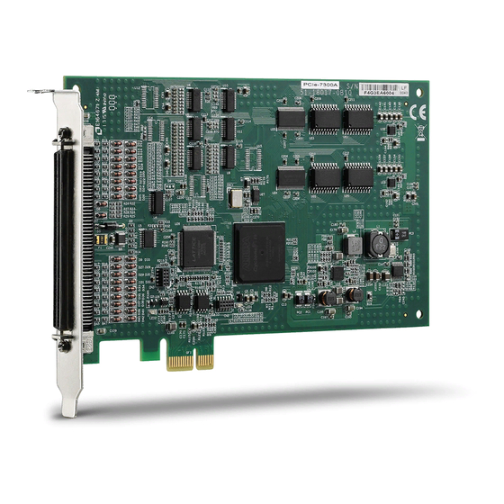
Page 21: Cpci/Pci/Pcie-7300A Layout
2.4 cPCI/PCI/PCIe-7300A Layout Figure 2-1: PCI-7300A Layout Diagram Installation... -
Page 22: Figure 2-2: Cpci-7300A Layout Diagram
Figure 2-2: cPCI-7300A Layout Diagram 167.65 Figure 2-3: PCIe-7300A Layout Diagram Installation... -
Page 23: Hardware Installation Outline
2.5 Hardware Installation Outline PCI configuration The cPCI/PCI/PCIe cards are equipped with plug and play PCI controller, it can request base addresses and interrupt accord- ing to PCI standard. The system BIOS will install the system resource based on the PCI cards’ configuration registers and system parameters (which are set by system BIOS). -
Page 24: Connector Pin Assignment
2.6 Connector Pin Assignment The PCI/cPCI/PCIe-7300A comes equipped with one 100-pin SCSI type connector (CN1) located on the rear mounting plate. The pin assignment of CN1 is illustrated in the Figure 2-3. Legend: Signa Pins Signal Name Signal Type Description Direction Ground –... - Page 25 Signa Pins Signal Name Signal Type Description Direction DI TRIG – can be used to control the DITRIG CONTROL start of data acquisition in all DI modes. AUX DI 3…0 – can be used as extra 78…81 AUXDI3…0 DATA input data or can be used as extra con- trol signals.
-
Page 26: Figure 2-4: Cn1 Pin Assignment
Figure 2-4: CN1 Pin Assignment Installation... -
Page 27: Wiring And Termination
These lines are capa- ble of inducing currents in or voltages on the cPCI/PCI/ PCIe-7300A if they run in parallel paths at a close dis- tance. To reduce the magnetic coupling between lines, separate them by a reasonable distance if they run in parallel, or run the lines at right angles to each other. -
Page 28: Termination Board Support
SCSI-100 connector. User can connect this daugh- ter board by a 100-pin SCSI type cable (ACL-102100) to the cPCI/ PCI/PCIe-7300A. It is suitable for the applications of 32-bit digital input or 32-bit digital output. 2.8.2 Connect with DIN-502S The DIN-502S with the cable ACL-10252 separates the 100-pin SCSI connector into two 50-pin SCSI connectors. -
Page 29: Registers
Registers In this chapter, the registers’ format of the cPCI/PCI/PCIe-7300A is described. This information is quite useful for the programmers who wish to handle the card by low-level programming. In addition, users can realize how to use software driver to manipulate this card after... -
Page 30: I/O Port Base Address
3.1 I/O Port Base Address The registers of the cPCI/PCI/PCIe-7300A are shown in Table 3.1. The base address of these registers is also assigned by the PCI P&P BIOS. The assigned base address is stored at offset 18h of the PCR. Therefore, users can read the PCR to know the base address by using BIOS function call. - Page 31 Legend: DI_CSR: Digital input control & status register DO_SCR: Digital output control & status register AUX_DIO: Auxiliary digital I/O port INT_CSR: Interrupt control and status register DI_FIFO: DI FIFO direct access port DO_FIFO: DO FIFO direct access port FIFO_CR: FIFO almost empty/full programming register POL_CTRL: Polarity control register for the control signals Caution: I/O port is 32-bit width...
-
Page 32: Di_Csr: Di Control & Status Register
3.2 DI_CSR: DI Control & Status Register Digital input control and status checking is done by this register. Address: BASE + 00 Attribute: READ/WRITE Data Format: Bit # 3-0 DI_HND_SHK DI_CLK_SEL DI_32 Bit # 7-4 PA_TERM_OFF DI_WAIT_TRIG -- (1) Bit # 11-8 DI_FIFO_FULL DI_OVER DI_FIFO_CLR... - Page 33 DI_EN (R/W) 0: Disable digital inputs 1: Enable digital inputs DI_FIFO_CLR (R/W) 0: No effect 1: Clear digital input FIFO. If both PORTA and PORTB are configured as inputs, both FIFO will be cleared. Always get 0 when read. DI_OVER (R/W) 0: DI FIFO does not full during input sampling 1: DI FIFO full during input sampling, some input data was lost, write “1”...
-
Page 34: Do_Csr: Do Control & Status Register
3.3 DO_CSR: DO Control & Status Register Digital input control and status checking is done by this register. Address: BASE + 04 Attribute: READ/WRITE Data Format: Bit # 3-0 DO_WAIT_NAE DO_MODE DO_32 Bit # 7-4 PG_STOP_TRIG PB_TERM_OFF DO_WAIT_TRG PAT_GEN Bit # 11-8 DO_FIFO_FULL DO_UNDER DO_FIFO_CLR... - Page 35 0: start output data immediately 1: delay output data until DOTRIG is actived PB_TERM_OFF (R/W) 0: PORTB terminator ON 1: PORTB terminator OFF PG_STOP_TRIG (R/W) 0: no effect 1: Stop pattern generation when DOTRIG is deasserted DO_EN (R/W) 0: Disable digital outputs 1: Enabled digital outputs DO_FIFO_CLR (R/W) 0:No effect...
-
Page 36: Auxiliary Digital I/O Register
3.4 Auxiliary Digital I/O Register Auxiliary 4-bit digital inputs and 4-bit digital outputs Address: BASE + 08 Attribute: READ/WRITE Data Format: Bit # 3-0 DO_AUX_3 DO_AUX_2 DO_AUX_1 DO_AUX_0 Bit # 7-4 DI_AUX_3 DI_AUX_2 DI_AUX_1 DI_AUX_0 Bit # 31-8 Don’t Care This auxiliary digital I/O is controlled by porgram I/O only. -
Page 37: Int_Csr: Interrupt Control And Status Register
3.5 INT_CSR: Interrupt Control and Status Register The interrupt of cPCI/PCI/PCIe-7300A is controlled and status is checked through this register. Address: BASE + 0x0C Attribute: READ/WRITE Data Format: Bit # 3-0 T2_INT AUXIO_INT T2_EN AUXDI0_EN Bit # 7-4 Reserved Reserved Bit # 31-8 Don’t Care... -
Page 38: Di_Fifo: Di Fifo Direct Access Port
3.6 DI_FIFO: DI FIFO direct access port The digital input FIFO data can be accessed through this port directly. Address: BASE + 0x10 Attribute: READ/WRITE Data Format: Bits 7 6 5 4 3 2 1 0 Bit # 7-0 DI_FIFO_8 Bit # 15-8 DI_FIFO_16 Bit # 31_16... -
Page 39: Do_Fifo: Do External Data Fifo Direct Access Port
3.7 DO_FIFO: DO external data FIFO direct access port The digital output FIFO data can be accessed through this port directly. Address: BASE + 0x0C Attribute: READ/WRITE Data Format: Bits 7 6 5 4 3 2 1 0 Bit # 7-0 DO_FIFO_8 Bit # 15-8 DO_FIFO_16... -
Page 40: Fifo_Cr: Fifo Almost Empty/Full Register
3.8 FIFO_CR: FIFO almost empty/full register The register is used to control the FIFO programmable almost empty/full flag. Address: BASE + 0x018 Attribute: WRITE Only Data Format: Bits 7 6 5 4 3 2 1 0 Bit 15-0 PB_PAE_PAF Bit 31_16 PA_PAE_PAF PB_PAE_PAF (WO) Programmable almost empty/full threshold of PORTB FIFO, 2... -
Page 41: Pol_Cntrl: Control Signal Polarity Control Register
3.9 POL_CNTRL: Control Signal Polarity Control Register The register is used to control the control signals’ polarity. control signals include DI_REQ, DI_ACK, DI_TRG, DO_REQ, DO_ACK and DO_TRG. Address: BASE + 0x1C Attribute: READ/WRITE Data Format: Bit # 3-0 DO_REG_NEG DI_TRG_NEG DI_ACK_NEG DI_REQ_NEG Bit # 71-4 DO_TRG_NEG DO_ACK_NEG... -
Page 42: Plx Pci-9080 Dma Control Registers
3.10 PLX PCI-9080 DMA Control Registers The registers of bus-mastering DMA as well as the control and status registers of PCI-bus interrupts are built in the PLX PCI-9080 ASIC. Users can refer to the manual of PLX PCI-9080 for detailed information. -
Page 43: Operation Theory
Operation Theory This chapter provides the detailed operation information for the cPCI/PCI/PCIe-7300A, including I/O configuration, block diagram, input/output FIFO, bus-mastering DMA, scatter/gather, clocking mode, starting mode, termination, I/O transfer mode, and auxiliary digital I/O. Operation Theory... -
Page 44: I/O Configuration
4.1 I/O Configuration The 32-bit I/O data path of PCI/cPCI/PCIe-7300A can be config- ured as 8-bit, 16-bit, or 32-bit, the possible configuration modes are listed as follows. Mode Channel Description PORTA (DI0…DI15) Both PORTA and PORTB are DI32 PORTB (DI16..DI31) configured as input channel PORTA (DO16…DO31) -
Page 45: Block Diagram
4.2 Block Diagram Figure 4-1 shows the block diagram of the cPCI/PCI/PCIe-7300A, it includes the I/O registers, two 16K FIFOs, auxiliary DIO, active terminators, and so on. Figure 4-1: Block diagram 16 Digital I/O Port, it can be set as terminated... -
Page 46: Digital I/O Data Flow
Figure 4-3: Data flow of digital output The width of local data bus on the cPCI/PCI/PCIe-7300A can be programmable to be 8-bit, 16-bit or 32-bit. The default data width is 16-bit. Port A is default to be input port, and Port B is default to be output one. -
Page 47: Input Fifo And Output Fifo
Due to the data transfer rate between external devices and the cPCI/PCI/PCIe-7300A is independent from that between cPCI/ PCI/PCIe-7300A and PCI bus. Two 16K words FIFO are provided to be I/O buffers. For digital input operation, data is sampled and transferred to the input FIFO. -
Page 48: Bus-Mastering Dma
PCI bus and the performance of each master will unavoidably drop. Therefore, in order to obtain the maximum data throughput of the cPCI/PCI/PCIe-7300A, it is recommended to remove or dis- able the bus mastering function of other bus masters, such as net- work, SCSI, modem adapters, and so on. - Page 49 hard-disk rather than memory, the bottleneck would be the data transfer rate of the hard-disk driver. Operation Theory...
-
Page 50: Scatter/Gather Dma
DMA descriptors altogether by their application programs. The cPCI/PCI/PCIe-7300A’s software driver provides the easy settings of the scatter/gather function, and some sample programs are also provided within the ADLINK all-in-one CD. Users can refer to these sample programs and the function 5.14 and 5.18 for more... -
Page 51: Clocking Mode
The specific sampling rate or the pacer rate can be program- mable by software, by external clock, or by easy handshaking pro- tocol. Four clocking modes are provided in the cPCI/PCI/PCIe-7300A to sample input data to the FIFO or output date from FIFO to the external devices. They are: 1. - Page 52 DO-ACK is asserted. That is, the external device can control the data input from the cPCI/PCI/PCIe-7300A by asserting the DO-ACK pin when it is ready to receive data.
-
Page 53: Starting Mode
4.8 Starting Mode Users can also control the starting mode of digital input and output by external signals (DITRIG and DOTRIG) with the software pro- grams. The trigger modes includes NoWait, WaitTRIG, WaitFIFO, and WaitBoth. 1. NoWait: The data transfer is started immediately when a I/O transfer command is issued. -
Page 54: Active Terminator
4.9 Active Terminator For cPCI/PCI/PCIe-7300A, it is important to terminate your cable properly to reduce or eliminate signal reflections in the cable. The PCI/cPCI/PCIe-7300A support active terminator on board, you can enable or disable the terminator by software selection. The active terminator is the same as the one used in SCSI 2. -
Page 55: Digital Input Operation Mode
4.10 Digital Input Operation Mode 4.10.1 Digital Input DMA in Internal Clock Mode There are three sources to trigger digital input in the internal clock mode: 20MHz, 10MHz, and programmable timer 82C54. There are three counters in 82C54, where the counter 0 is used for sam- pling clock source for digital input. - Page 56 Note: When the DMA function of digital input starts, the input data will be stored in the FIFO of the cPCI/PCI/PCIe-7300A. The data then transfer to system memory if PCI bus is available. If the speed of translation from external device to the FIFO...
-
Page 57: Digital Input Dma In External Clock Mode
DMA. 7. The DI-ACK signal indicates the status of the cPCI/PCI/ PCIe-7300A’s input FIFO is in external clock mode. When the digital input circuit of cPCI/PCI/PCIe-7300A is enabled and its FIFO is not almost full, the DIACK signal will remain asserted. -
Page 58: Figure 4-7: Direq As Input Data Strobe (Rising Edge Active)
The operation flow is show as below: The followings are timing diagrams of the DI-REQ and the input data. The active edge of DI-REQ can be programmed by the func- tion 5.5. Figure 4-7: DIREQ as input data strobe (Rising Edge Active) Operation Theory... -
Page 59: Digital Input Dma In Handshaking Mode
Figure 4-8: DIREQ as input data strobe (Falling Edge Active) Note: From the timing diagram of external clock mode, the maxi- mum frequency can be up to 40MHz. However, users should note that when the sampling frequency of digital input is higher than the PCI bus bandwidth (33Mhz), or the band- width of chipset (30Mhz typically) from PCI bus to system memory. - Page 60 5. After digital input data is ready on device side, the peripheral device strobe data into the cPCI/PCI/PCIe- 7300A by asserting a DIREQ signal, 6. The DIREQ signal caused the cPCI/PCI/PCIe-7300A to latch digital input data and store it into FIFO 7. The cPCI/PCI/PCIe-7300A asserts a DIACK signal when it is ready for another input, the step 5 to step 7 will be repeated again.
-
Page 61: Continuous Digital Input
If the digital input operation still active after the competition of the previous DMA transfer and do not clear the data in the input FIFO when the next DMA starts, the cPCI/PCI/PCIe-7300A can achieve the continuous digital input function in a high-speed sampling rate. - Page 62 and remove the unnecessary processes in your applica- tion programs. 3. When high-speed sampling frequency is applied, the larger block size will improve the efficiency of DMA transferring, and probability of overrun in the DMA pro- cess will be reduced. 4.
-
Page 63: Digital Output Operation Mode
4.11 Digital Output Operation Mode 4.11.1 Digital Output DMA in Internal Clock Mode There are three sources to trigger digital output: 20MHz, 10MHz, and programmable timer 82C54. There are three counters in 82C54, where the counter 1 is used timer pacer for digital output. The operations sequence of digital output with internal clock are listed: 1. -
Page 64: Digital Output Dma In Handshaking Mode
As the data output in the internal clock mode, the DOREQ signal could be use as the output strobe to indicate the output operation to the external device. The timing diagram of the DOREQ is shown as follows: Figure 4-10: DOREQ as output data strobe 4.11.2 Digital Output DMA in Handshaking Mode For digital output, through DO-REQ output signal and DO-ACK input signal, the digital output can have simple handshaking data... - Page 65 The operations sequence of digital output in handshaking mode are listed: 1. Define the input configuration to be 32-bit, 16-bit or 8-bit data width. 2. Enable or disable the active terminators. 3. Define the output clock mode as handshaking mode. Connect the handshaking signals of the external device to output pin DO-REQ and input pin DO-ACK.
-
Page 66: Digital Output Dma In Burst Handshaking Mode
The timing diagram of the DOREQ and DOACK in the DO hand- shaking mode is shown as follows: Figure 4-11: DOREQ & DOACK Handshaking Note: DOACK must be deserted before DOREQ asserts, DOACK can be asserted any time after DOREQ asserts, DOREQ will be reasserted after DOACK is asserted. - Page 67 The operations sequence of digital output in burst handshaking mode are listed: 1. Define the input configuration to be 32-bit, 16-bit or 8-bit data width. 2. Enable or disable the active terminators. 3. Define the output clock as burst handshaking mode and decide the timer pacer rate to be 20Mhz, 10Mhz, or the output of 82C54 timer 1.
- Page 68 Note: When the DMA function of digital output starts, the output data will transfer to the output FIFO of cPCI/PCI/PCIe-7300A when PCI bus is available. If the speed of translation from the FIFO on board to the external device is higher than that...
-
Page 69: Pattern Generator
The digital data is output to the peripheral device periodically based on the clock signals occur at a constant rate. The digital pattern are stored in the cPCI/PCI/PCIe-7300A’s on-board FIFO with the length of pattern less than or equal to 16K samples. -
Page 70: Auxiliary Dio
4.12 Auxiliary DIO The cPCI/PCI/PCIe-7300A also includes four auxiliary digital inputs and four digital outputs, which can be applied to achieve the simple I/O functions. Users can refer to the functions 5.8 - 5.11 for the detailed information. Operation Theory... -
Page 71: C++ Libraries
C/C++ Libraries This chapter describes the software library for operating this card. Only the functions in DOS library and Windows 95 DLL are described. Please refer to the PCIS-DASK function reference manual, which included in ADLINK CD, for the descriptions of the Windows 98/NT/2000/Vista DLL functions. -
Page 72: Libraries Installation
5.1 Libraries Installation Please refer to the “Software Installation Guide” for the detail infor- mation about how to install the software libraries for DOS, or Win- dows 95 DLL, or PCIS-DASK for Windows 98/NT/2000. The device drivers and DLL functions of Windows 98/NT/2000 are included in the PCIS-DASK. -
Page 73: Programming Guide
The naming convention rules are: In DOS Environment: _{hardware_model}_{action_name}. e.g. _7300_Initial(). All functions in cPCI/PCI/PCIe-7300A driver are with 7300 as {hardware_model}. But they can be used by cPCI/PCI/PCIe- 7300A, cPCI-7300. In order to recognize the difference between DOS library and Win- dows 95 library, a capital "W"... -
Page 74: 7300_Initial
5.3 _7300_Initial @ Description A cPCI/PCI/PCIe-7300A card is initialized according to the card number. Because the cPCI/PCI/PCIe-7300A is PCI bus architec- ture and meets the plug and play design, the IRQ and base address (pass-through address) are assigned by system BIOS directly. - Page 75 irq_no:system will give an available interrupt number to this card automatically. pci_master:TRUE: BIOS enabled PCI bus mastering FALSE: BIOS did not enable PCI bus mastering @ Return Code NoError, PCICardNumErr PCIBiosNotExistPCICardNotExist PCIBaseAddrErr C/C++ Libraries...
-
Page 76: 7300_Close
5.4 _7300_Close @ Description Close a previously initialized cPCI/PCI/PCIe-7300A card. @ Syntax Visual C/C++ (Windows 95) int W_7300_Close (int card_number) Visual Basic (Windows 95) W_7300_Close (ByVal card_number As Long) As Long C/C++ (DOS) int _7300_Close (int card_number) @ Argument card_number:The card number of the cPCI/PCI/PCIe-7300A card. -
Page 77: 7300_Configure
5.5 _7300_Configure @ Description Set the port DI/O configuration, terminator control, and control sig- nal polarity for the cPCI/PCI/PCIe-7300A card. @ Syntax Visual C/C++ (Windows 95) int W_7300_Configure (int card_number, int dio_config, int term_cntrl, int cntrl_pol) Visual Basic (Windows 95) - Page 78 PAON_PBOFF: PORTA terminator ON, PORTB terminator PAON_PBON: PORTA terminator ON, PORTB terminator Note: term_cntrl is used to control the ON/OFF of the active termi- nators, not terminal power output: TERMPER) cntrl_pol:The polarity configuration. This argument is an inte- ger expression formed from one or more of the manifest constants defined in 7300.h.
-
Page 79: 7300_Di_Mode
5.6 _7300_DI_Mode @ Description Set the clock mode and start mode for the cPCI/PCI/PCIe-7300A DI operation. @ Syntax Visual C/C++ (Windows 95) int W_7300_DI_Mode (int card_number, int clk_mode, int start_mode) Visual Basic (Windows 95) W_7300_DI_Mode (ByVal card_number As Long, ByVal... -
Page 80: 7300_Do_Mode
5.7 _7300_DO_Mode @ Description Set the clock mode and start mode for the cPCI/PCI/PCIe-7300A DO operation. @ Syntax Visual C/C++ (Windows 95) int W_7300_DO_Mode (int card_number, int clk_mode, int start_mode, int fifo_threshold) Visual Basic (Windows 95) W_7300_DO_Mode (ByVal card_number As Long, ByVal... - Page 81 DO_WAIT_FIFO: delay output data until FIFO is not almost empty DO_WAIT_BOTH: delay output data until DOTRIG is active and FIFO is not almost empty. fifo_threshold:programmable almost empty threshold of both PORTB FIFO and PORTA FIFO (if PORTA is set as output). It is avaliavle only when start_mode is DO_WAIT_FIFO @ Return Code NoError...
-
Page 82: 7300_Aux_Di
W_7300_AUX_DI (ByVal card_number As Long, aux_di As Long) As Long C/C++ (DOS) int _7300_AUX_DI (int card_number, int *aux_di) @ Argument card_number:The card number of the cPCI/PCI/PCIe-7300A card. aux_di:returns 4-bit value from auxiliary digital input port. @ Return Code NoError PCICardNumErr... -
Page 83: 7300_Aux_Di_Channel
@ Description Read data from auxiliary digital input channel. There are 4 digital input channels on the cPCI/PCI/PCIe-7300A auxiliary digital input port. When performs this function, the auxiliary digital input port is read and the value of the corresponding channel is returned. -
Page 84: 7300_Aux_Do
W_7300_AUX_DI (ByVal card_number As Long, ByVal do_data As Long) As Long C/C++ (DOS) int _7300_AUX_DI (int card_number, int do_data) @ Argument card_number:The card number of the cPCI/PCI/PCIe-7300A card. do_data:value will be written to auxiliary digital output port @ Return Code NoError... -
Page 85: 7300_Aux_Do_Channel
5.11 _7300_AUX_DO_Channel @ Description Write data to auxiliary digital output channel (bit). There are 4 aux- iliary digital output channels on the cPCI/PCI/PCIe-7300A. When performs this function, the digital output data is written to the cor- responding channel. * channel means each bit of digital output port. -
Page 86: 7300_Alloc_Dma_Mem
5.12 _7300_Alloc_DMA_Mem @ Description Contact Windows 95 system to allocate a memory for DMA trans- fer. This function is only available in Windows 95 version. @ Syntax Visual C/C++ (Windows 95) int W_7300_Alloc_DMA_Mem (U32 buf_size, HANDLE *memID, U32 *linearAddr) Visual Basic (Windows 95) W_7300_Alloc_DMA_Mem (ByVal buf_size As Long, memID As Long, linearAddr As Long) As Long @ Argument... -
Page 87: 7300_Free_Dma_Mem
5.13 _7300_Free_DMA_Mem @ Description Deallocate a system DMA memory under the Windows 95 envi- ronment. This function is only available in the Windows 95 version. @ Syntax Visual C/C++ (Windows 95) int W_7300_Free_DMA_Mem (HANDLE memID) Visual Basic (Windows 95) W_7300_Free_DMA_Mem (ByVal memID As Long ) As Long @ Argument memID:The memory ID of the system DMA memory to deallocate. -
Page 88: 7300_Di_Dma_Start
After executing this function, it is necessary to check the status of the operation by using the function _7300_DI_DMA_Status. The cPCI/PCI/PCIe-7300A bus mastering DMA is different from tradi- tional PC style DMA. Its description is as follows: Bus Mastering DMA mode of cPCI/PCI/PCIe-7300A: PCI bus mastering offers the highest possible speed available cPCI/PCI/PCIe-7300A. - Page 89 transfers are always longwords, this is 2 million long- words (2^21). 3. After the input sampling is started, the input data is stored in the FIFO of PCI controller. Each bus mastering data transfer continually tests if any data in the FIFO and then blocks transfer, the system will continuously loop until the conditions are satisfied again but will not exit the block transfer cycle if the block count is not complete.
- Page 90 (DOS):CHAIN_DMA: chaining DMA mode. By using the scatter-gather capability of cPCI/PCI/PCIe-7300A, the input data is put to several buffers which chained together. NON_CHAIN_DMA: The input data is stored in a block of contiguous memory.
- Page 91 disable_di:0: digital input operation still active after DMA trans- fer complete 1: disable digital input operation immediately when DMA transfer complete @ Return Code NoError PCICardNumErr PCICardNotInit DMATransferNotAllowed InvalidDIOCount BufNotDWordAlign DMADscrBadAlign C/C++ Libraries...
-
Page 92: 7300_Di_Dma_Status
As Long) As Long C/C++ (DOS) int _7300_DI_DMA_Status (int card_number, int *status) @ Argument card_number:The card number of the cPCI/PCI/PCIe-7300A card. status: status of the DMA data transfer 0 (DMA_DONE): DMA is completed 1 (DMA_CONTINUE): DMA is not completed... -
Page 93: 7300_Di_Dma_Abort
Visual C/C++ (Windows 95) int W_7300_DI_DMA_Abort (int card_number) Visual Basic (Windows 95) W_7300_DI_DMA_Abort (ByVal card_number As Long ) As Long C/C++ (DOS) int _7300_DI_DMA_Stop (int card_number) @ Argument card_number:The card number of the cPCI/PCI/PCIe-7300A card. @ Return Code NoError PCICardNumErr PCICardNotInit C/C++ Libraries... -
Page 94: 7300_Getoverrunstatus
W_7300_GetOverrunStatus (ByVal card_number As Long, overrun As Long) As Long C/C++ (DOS) int _7300_GetOverrunStatus (int card_number, int *overrun) @ Argument card_number:The card number of the cPCI/PCI/PCIe-7300A card. overrun:0: overrun sitation did not occur. 1: overrun situation occurred. @ Return Code NoError... -
Page 95: 7300_Do_Dma_Start
ByVal memID As Long, ByVal count As Long) As Long C/C++ (DOS) int _7300_DO_DMA_Start (int card_number, U32 *buff, U32 count, int repeat, DMA_DSCR *dma_dscr_ptr) @ Argument card_number:The card number of the cPCI/PCI/PCIe-7300A card. memID (Win-95): the memory ID of the allocated system DMA memory. Windows environment, before... - Page 96 ** This memory should be double-word alignment count:For non-chaining mode, this is the total number of digital output data in double-words (4-byte). The value of count can not exceed 2^21 (about 2 million). For chaining mode, please set this argument as 0. The number of digital output is determined by the information in DMA descriptor nodes.
-
Page 97: 7300_Do_Dma_Status
As Long) As Long C/C++ (DOS) int _7300_DO_DMA_Status (int card_number, int *status) @ Argument card_number:The card number of the cPCI/PCI/PCIe-7300A card. status: status of the DMA data transfer 0 (DMA_DONE): DMA is completed 1 (DMA_CONTINUE): DMA is not completed... -
Page 98: 7300_Do_Dma_Abort
Visual C/C++ (Windows 95) int W_7300_DO_DMA_Abort (int card_number) Visual Basic (Windows 95) W_7300_DO_DMA_Abort (ByVal card_number As Long) As Long C/C++ (DOS) int _7300_DO_DMA_Abort (int card_number) @ Argument card_number:The card number of the cPCI/PCI/PCIe-7300A card. @ Return Code NoError PCICardNumErr PCICardNotInit C/C++ Libraries... -
Page 99: 7300_Do_Pg_Start
C/C++ (DOS) int _7300_DO_PG_Start (int card_number, void *buff_ptr, U32 count) @ Argument card_number:The card number of the cPCI/PCI/PCIe-7300A card. buff_ptr:the start address of the memory buffer to store the out- put data of pattern generation. ** This memory should be double-word alignment count:the total number of pattern generation samples. - Page 100 BufNotDWordAlign DMADscrBadAlign C/C++ Libraries...
-
Page 101: 7300_Do_Pg_Stop
Visual C/C++ (Windows 95) int W_7300_DO_PG_Stop (int card_number) Visual Basic (Windows 95) W_7300_DO_PG_Stop (ByVal card_number As Long) As Long C/C++ (DOS) int _7300_DO_PG_Stop (int card_number) @ Argument card_number:The card number of the cPCI/PCI/PCIe-7300A card. @ Return Code NoError PCICardNumErr PCICardNotInit C/C++ Libraries... -
Page 102: 7300_Di_Timer
W_7300_DI_Timer (ByVal card_number As Long, ByVal c0 As Integer) As Long C/C++ (DOS) int _7300_DI_Timer (int card_number, U16 c0) @ Argument card_number:The card number of the cPCI/PCI/PCIe-7300A card. c0: frequency divider of Counter #0. Valid value ranges from 2 to 65535. Note: Since the Integer type in Visual Basic is signed integer. -
Page 103: 7300_Do_Timer
W_7300_DO_Timer (ByVal card_number As Long, ByVal c1 As Integer) As Long C/C++ (DOS) int _7300_DO_Timer (int card_number, U16 c1) @ Argument card_number:The card number of the cPCI/PCI/PCIe-7300A card. c1: frequency divider of Counter #1. Valid value ranges from 2 to 65535. Note: Since the Integer type in Visual Basic is signed integer. -
Page 104: 7300_Int_Timer
W_7300_Int_Timer (ByVal card_number As Long, ByVal c2 As Integer) As Long C/C++ (DOS) int _7300_Int_Timer (int card_number, U16 c2) @ Argument card_number:The card number of the cPCI/PCI/PCIe-7300A card. c2: frequency divider of Counter #2. Valid value ranges from 2 to 65535. Note: Since the Integer type in Visual Basic is signed integer. -
Page 105: 7300_Get_Sample
5.26 _7300_Get_Sample @ Description For the language without pointer support such as Visual Basic, programmer can use this function to access the index-th data in input DMA buffer. This function is only available in Windows 95 version. @ Syntax Visual C/C++ (Windows 95) int W_7300_Get_Sample (U32 linearAddr, U32 index, U32 *data_value, U32 portWidth) Visual Basic (Windows 95) -
Page 106: 7300_Set_Sample
5.27 _7300_Set_Sample @ Description For the language without pointer support such as Visual Basic, programmer can use this function to write the output data to the index-th position in output DMA buffer. This function is only avail- able in Windows 95 version. @ Syntax Visual C/C++ (Windows 95) int W_7300_Set_Sample (U32 linearAddr, U32 index,... -
Page 107: 7300_Getunderrunstatus
@ Description When you use _7300_DO_DMA_Start to output data, the output data is read from the FIFO on the cPCI/PCI/PCIe-7300A. If the FIFO becomes empty and next data is read from the FIFO, under- run situation occurs. Using this function to check underrun status. - Page 108 C/C++ Libraries...
-
Page 109: Appendix
Appendix 8254 Programmable Interval Timer Note: The material of this section is adopted from “Intel Micropro- cessor and Peripheral Handbook Vol. II --Peripheral” The Intel (NEC) 8254 The Intel (NEC) 8254 contains three independent, programmable, multi-mode 16 bit counter/timers. The three independent 16 bit counters can be clocked at rates from DC to 5 MHz. - Page 110 Control Byte: (Base + 7, Base + 11) SC1 SC0 RL1 RL0 M2 M1 M0 BCD SC1 & SC1 - Select Counter (Bit7 & Bit 6) SC1 SC0 COUNTER ILLEGAL RL1 & RL0 - Select Read/Load operation (Bit 5 & Bit 4) RL1 RL0 OPERATION COUNTER LATCH...
-
Page 111: Mode Definition
2. The count of the BCD counter is from 0 up to 99,999. Mode Definition In 8254, there are six different operating modes can be selected. They are: Mode 0: Interrupt on terminal count The output will be initially low after the mode set operation. After the count is loaded into the selected count register, the output will remain low and the counter will count. - Page 112 The gate input when low, will force the output high. When the gate input goes high, the counter will start form the initial count. Thus, the gate input can be used to synchronized by software. When this mode is set, the output will remain high until after the count register is loaded.
- Page 113 Mode 5: Hardware Triggered Strobe. The counter will start counting after the rising edge of the trig- ger input and will go low for one clock period when the terminal count is reached. The counter is re-triggerable. the output will not go low until the full count after the rising edge of any trigger.
- Page 114 Appendix...
Need help?
Do you have a question about the PCIe-7300A and is the answer not in the manual?
Questions and answers