Texas Instruments TPS6594-Q1 Series User Manual
Evaluation module
Hide thumbs
Also See for TPS6594-Q1 Series:
- User manual (43 pages) ,
- User manual (48 pages) ,
- User manual (51 pages)
Table of Contents
Advertisement
Quick Links
The TPS6594x-Q1 Evaluation Module (EVM) highlights the performance and flexibility of the TPS6594x-
Q1 power management integrated circuit (PMIC). The modular design allows the EVMs to be stacked to
provide a multi-PMIC solution with a single PMIC acting as the master and up to five PMIC slaves. This
document should be used in conjunction with the Programmable Processor PMIC's GUI User's Guide
SLVUBT8
and the TPS6594x-Q1 Power Management IC (PMIC) with 4-phase 14-A Buck for Processors
SLVSEA7.
...................................................................................................................
1
2
2.1
2.2
2.3
3
3.1
3.2
3.3
3.4
3.5
3.6
3.7
4
4.1
4.2
Changing the Phase Configuration
5
Additional Resources
6
Schematic, Layout, and Bill of Materials
.................................................................................................................
7
Typical Data
....................................................................................................................
8
EMI Data
9
Thermal Data
1
EVM Top View
2
EVM Header J7
3
LDO Headers
4
EVM Masters Slave Configuration
5
EVM Bottom View
6
Header J37, Recommended Power Sequence (Enable) for Master and One or More Slaves
7
Interface Settings for I
8
9
10
Schematic Page 1
11
Schematic Page 2
12
13
14
Submit Documentation Feedback
...............................................................................................................
......................................................................................
........................................................................................................
..................................................................................................................
.....................................................................................................
............................................................................................
.............................................................................................
......................................................................................................
...................................................................................................
.........................................................................................................
...............................................................................................................
......................................................................................................
................................................................................
...............................................................................................................
...............................................................................................................
..............................................................................................................
.................................................................................................................
.........................................................................................
..........................................................................................................
2
.......................................................................................
..........................................................................................................
..........................................................................................................
........................................................................................................
..................................................................................................
.....................................................................................................
Copyright © 2019, Texas Instruments Incorporated
TPS6594x-Q1 Evaluation Module
Contents
.......................................................................
................................................................
........................................................................
.............................................................................
List of Figures
...............................................................................
..............................................................................
User's Guide
SLVUBT0 - December 2019
..................
TPS6594x-Q1 Evaluation Module
3
3
3
4
4
5
5
5
6
8
9
12
12
12
12
14
15
16
27
27
27
4
6
8
9
10
11
13
14
15
16
17
18
19
20
1
Advertisement
Table of Contents

Subscribe to Our Youtube Channel
Related Manuals for Texas Instruments TPS6594-Q1 Series


Summary of Contents for Texas Instruments TPS6594-Q1 Series
-
Page 1: Table Of Contents
Phase Configuration Components ......................Schematic Page 1 ......................Schematic Page 2 ......................Layout Top, Layer 1 ....................Layout Ground, Layer 2 ..................... Layout Signal, Layer 3 SLVUBT0 – December 2019 TPS6594x-Q1 Evaluation Module Submit Documentation Feedback Copyright © 2019, Texas Instruments Incorporated... - Page 2 Header J15, USB_3V3/VSYS/VBUS, GPIO1/I2C/SPI ....................Header J8 Pullup Voltages ..................Header J37 Master/Slave Select ....................... EVM LED Indicators ................Bill of Materials of Balance of Components TPS6594x-Q1 Evaluation Module SLVUBT0 – December 2019 Submit Documentation Feedback Copyright © 2019, Texas Instruments Incorporated...
-
Page 3: Introduction
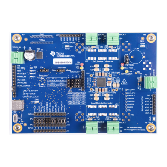
ON Request for the master device is the ENABLE pin which is a level sensitive input. Please refer SLVSEA7 for more details. Figure 1 shows the TPS659413EVM (master). SLVUBT0 – December 2019 TPS6594x-Q1 Evaluation Module Submit Documentation Feedback Copyright © 2019, Texas Instruments Incorporated... -
Page 4: Getting Started: Multiple Evm Evaluation
J28. The power supply can be applied to any of the available J6 terminals. The GUI Tool Texas Instruments provides a GUI tool to enable, configure, and evaluate the various features of the TPS6594x-Q1 with the EVM. Please refer to the GUI User's Guide... -
Page 5: Evm Details
TP10 SW_B2 TP11 SW_B3 TP12 SW_B4 TP13 SW_B5 TP14 Section 3.4 for applying input voltages other than VSYS_IN to the LDO regulators through J21 SLVUBT0 – December 2019 TPS6594x-Q1 Evaluation Module Submit Documentation Feedback Copyright © 2019, Texas Instruments Incorporated... -
Page 6: Configuration Headers
SoC Error Count Down mode. GPIO3 of the PMIC should be in the Alternative function to support the system error count down from the SoC. GPIO is connected to alternative MCU output, nERR_SoC. TPS6594x-Q1 Evaluation Module SLVUBT0 – December 2019 Submit Documentation Feedback Copyright © 2019, Texas Instruments Incorporated... - Page 7 SPI mode, Chip Select. GPIO1 of the PMIC should be in the Alternative function to support SPI communication. This setting is done in conjunction with J7, GPIO2, SDA2/SDO: Closed SLVUBT0 – December 2019 TPS6594x-Q1 Evaluation Module Submit Documentation Feedback Copyright © 2019, Texas Instruments Incorporated...
-
Page 8: Signal Headers
10 kΩ resistor pullup. J10 (PD) is located directly below J9 to enable shorting each GPIO directly to GND. TPS6594x-Q1 Evaluation Module SLVUBT0 – December 2019 Submit Documentation Feedback Copyright © 2019, Texas Instruments Incorporated... -
Page 9: Stack-Up Headers
J27 and J28. Communication between the boards is shared on header J29. This header, J29, is marked on the bottom silkscreen, as shown in Figure Figure 4. EVM Masters Slave Configuration SLVUBT0 – December 2019 TPS6594x-Q1 Evaluation Module Submit Documentation Feedback Copyright © 2019, Texas Instruments Incorporated... - Page 10 When in master mode or when the header J37 is left open the nPWRON/ENABLE pin can be controlled with the EVM push button and S1. TPS6594x-Q1 Evaluation Module SLVUBT0 – December 2019 Submit Documentation Feedback Copyright © 2019, Texas Instruments Incorporated...
- Page 11 M/S Select, Master: Closed Master Mode. The PMIC signal, VOUT_LDOVINT, is connected to the nPWRON_S which will be the ENABLE signal on the PMICs connected as slaves. SLVUBT0 – December 2019 TPS6594x-Q1 Evaluation Module Submit Documentation Feedback Copyright © 2019, Texas Instruments Incorporated...
-
Page 12: Connectors
The default settings for communication with the PMIC is I C. This default configuration for GPIO1 and GPIO2 are the function settings SCL_I2C2 and SDA_I2C2, respectively. TPS6594x-Q1 Evaluation Module SLVUBT0 – December 2019 Submit Documentation Feedback Copyright © 2019, Texas Instruments Incorporated... -
Page 13: Communication
GUI (through the micro controller). All other EVMs which are stacked should pull GPIO1 high, so that the PMIC does not respond or interfere with the SPI communication. SLVUBT0 – December 2019 TPS6594x-Q1 Evaluation Module Submit Documentation Feedback Copyright © 2019, Texas Instruments Incorporated... -
Page 14: Interface Settings For Spi Communication
TP6 and TP7 respectively. If the voltage monitors associated with BUCK3 and BUCK4 are disabled, then it is recommended to connect the FB_Bn pins to reference ground, using R4 and R6. TPS6594x-Q1 Evaluation Module SLVUBT0 – December 2019 Submit Documentation Feedback Copyright © 2019, Texas Instruments Incorporated... -
Page 15: Phase Configuration Components
Programmable Processor PMIC's GUI User’s Guide • TPS65921-Q1 Power Management IC (PMIC) With 4-Phase 14-A Buck for ProcessorsTPS65921-Q1 Power Management IC (PMIC) With 4-Phase 14-A Buck for Processors SLVUBT0 – December 2019 TPS6594x-Q1 Evaluation Module Submit Documentation Feedback Copyright © 2019, Texas Instruments Incorporated... -
Page 16: Schematic
J37-1-2 to get power on signal (ENABLE) from master. VSYS VOUT_B5 No jumper on J37 when single PMIC is used. +VBUS GNDS VCCA_S SCL_I2C2/CS_SPI GNDS GPIO1 GNDS Figure 10. Schematic Page 1 TPS6594x-Q1 Evaluation Module SLVUBT0 – December 2019 Submit Documentation Feedback Copyright © 2019, Texas Instruments Incorporated... - Page 17 SDA2/SDO SPI_MISO 2.2uF C109 PUEN 2.2uF 2.2uF SCL2 SCL2/CS SPI_CS C107 VCCA 0.1uF 1.0M 1.0M 1.0M I2C_SPI_SEL C108 0.47uF Figure 11. Schematic Page 2 SLVUBT0 – December 2019 TPS6594x-Q1 Evaluation Module Submit Documentation Feedback Copyright © 2019, Texas Instruments Incorporated...
-
Page 18: Layout Top, Layer
Schematic, Layout, and Bill of Materials www.ti.com Figure 12. Layout Top, Layer 1 TPS6594x-Q1 Evaluation Module SLVUBT0 – December 2019 Submit Documentation Feedback Copyright © 2019, Texas Instruments Incorporated... -
Page 19: Layout Ground, Layer
Schematic, Layout, and Bill of Materials www.ti.com Figure 13. Layout Ground, Layer 2 SLVUBT0 – December 2019 TPS6594x-Q1 Evaluation Module Submit Documentation Feedback Copyright © 2019, Texas Instruments Incorporated... -
Page 20: Layout Signal, Layer
Schematic, Layout, and Bill of Materials www.ti.com Figure 14. Layout Signal, Layer 3 TPS6594x-Q1 Evaluation Module SLVUBT0 – December 2019 Submit Documentation Feedback Copyright © 2019, Texas Instruments Incorporated... -
Page 21: Layout Signal, Layer
Schematic, Layout, and Bill of Materials www.ti.com Figure 15. Layout Signal, Layer 4 SLVUBT0 – December 2019 TPS6594x-Q1 Evaluation Module Submit Documentation Feedback Copyright © 2019, Texas Instruments Incorporated... -
Page 22: Layout Ground, Layer
Schematic, Layout, and Bill of Materials www.ti.com Figure 16. Layout Ground, Layer 5 TPS6594x-Q1 Evaluation Module SLVUBT0 – December 2019 Submit Documentation Feedback Copyright © 2019, Texas Instruments Incorporated... -
Page 23: Layout Bottom
Schematic, Layout, and Bill of Materials www.ti.com Figure 17. Layout Bottom SLVUBT0 – December 2019 TPS6594x-Q1 Evaluation Module Submit Documentation Feedback Copyright © 2019, Texas Instruments Incorporated... -
Page 24: Terminal Blocks
Terminal Block, 5 1792863 mm, 2x1, R/A, TH mm, 2x1, R/A, TH J7, J8, J9, J10, J11, Header, 100 mil, 11x1 Header TSW-111-07-G-S 11x1, Gold, TH TPS6594x-Q1 Evaluation Module SLVUBT0 – December 2019 Submit Documentation Feedback Copyright © 2019, Texas Instruments Incorporated... -
Page 25: Header J7 Description
RES, 1.0 M, 5%, 0402 CRCW04021M00JNE 0.063 W, AEC-Q200 Grade 0, 0402 R53, R56, R57 200 k RES, 200 k, 5%, 0402 CRCW0402200KJNE 0.063 W, 0402 SLVUBT0 – December 2019 TPS6594x-Q1 Evaluation Module Submit Documentation Feedback Copyright © 2019, Texas Instruments Incorporated... - Page 26 DSE0006A (WSON- U7, U10 0.5 Ω Dual SPDT RSW0010A TS3A5223RSWR Bidirectional Analog Switch, RSW0010A (UQFN-10) U8, U9 8-BIT PW0020A SN74GTL2003PWR BIDIRECTIONAL LOW-VOLTAGE TRANSLATOR, PW0020A (TSSOP- TPS6594x-Q1 Evaluation Module SLVUBT0 – December 2019 Submit Documentation Feedback Copyright © 2019, Texas Instruments Incorporated...
-
Page 27: Bill Of Materials Of Balance Of Components
0.063 W, AEC-Q200 Grade 0, 0402 TP9, TP10, TP11, Test Point, Miniature, Yellow Miniature 5004 TP12, TP13 Yellow, TH Testpoint Typical Data EMI Data Thermal Data SLVUBT0 – December 2019 TPS6594x-Q1 Evaluation Module Submit Documentation Feedback Copyright © 2019, Texas Instruments Incorporated... - Page 28 TI products. TI’s provision of these resources does not expand or otherwise alter TI’s applicable warranties or warranty disclaimers for TI products. Mailing Address: Texas Instruments, Post Office Box 655303, Dallas, Texas 75265 Copyright © 2019, Texas Instruments Incorporated...
Need help?
Do you have a question about the TPS6594-Q1 Series and is the answer not in the manual?
Questions and answers