Table of Contents
Advertisement
Quick Links
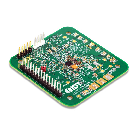
P9412
Wireless Power TRx WattShare
Description
The P9412 CSP TRx evaluation board can be used
to demonstrate the features and performance of the
P9412 Wireless Power Transceiver solution for
Mobile Device with a custom Rx only or TRx coils.
The intuitive top-level placement of components,
layout, and controls simplify the design-in process,
optimizes the user experience, and emphasizes the
impressive level of integration and abundance of
useful features that this device offers.
The device is powered by a Renesas Proprietary
TRx coil that can be copied when used with
Renesas products (Worldwide patent pending). The
P9412 operates in RX mode or TX mode depending
on the setting and the firmware loaded to its
Multiple-Time Programmable memory (MTP).
2
J3 pin I
C Access
for MTP / Registers
J8, J9 pins
for test points
V1P8_AP
input
P9412
V5P0_AP
input
Rev.1.7
Jul.8.20
TM
Solution for Wireless Charging for Wireless Power Charging
Figure 1. P9412 CSP Demo Board v1.3
P9412 Evaluation Board Manual
Features
P9412 CSP TRx WattShare
•
Solution
Delivers over 30W output power as a Receiver
•
Delivers over 6W output power as Transmitter
•
Integrated high-performance capacitor divider
•
XY Position Sensing Technology
•
I2C Connector
•
Multiple-Time Programmable Memory (MTP)
•
Fully assembled with test points and coil fixture
•
6-layer PCB with 1oz. copper
•
TM
Wireless power
SMD Test Points
CPOUT Output
to load
CPOUTS for
Kelvin sensing
WPC TRx
Coil inputs
Page 1
Advertisement
Table of Contents

Subscribe to Our Youtube Channel
Related Manuals for Renesas P9412


Summary of Contents for Renesas P9412
-
Page 1: Figure 1. P9412 Csp Demo Board V1.3
P9412 Wireless Power TRx WattShare Solution for Wireless Charging for Wireless Power Charging Description Features The P9412 CSP TRx evaluation board can be used P9412 CSP TRx WattShare Wireless power • Solution to demonstrate the features and performance of the... -
Page 2: Table Of Contents
Usage Guide ..............................7 Quick-Start Guide for Rx and Tx Mode Operation ................7 Using the Windows GUI ........................8 1.2.1. Using the GUI to Program the P9412 ..................8 1.2.2. Using the GUI to Read / Write to Registers ................12 1.2.3. - Page 3 P9412 Evaluation Board Manual 2.1.5.7. TRX Data Value 1~2 Register (PropPkt Received), TRX_Data_Value1_2_In (0x59, 0x5A) ... 34 2.1.5.8. Com Channel Send Size Register, CC_Send_Size_L (0x140), CC_Send_Size_H (0x141) ... 34 2.1.5.9. Com Channel Send Index Register, CC_Send_Index_L (0x142), CC_Send_Index_H (0x143) ..34 2.1.5.10.
- Page 4 P9412 Evaluation Board Manual 2.1.10.2. EPP Q-Factor A Register, EPP_Q_Fact_A (0x138) ..............46 2.1.10.3. EPP Q-Factor B Register, EPP_Q_Fact_B (0x139) ..............46 2.1.10.4. EPP TX Guaranteed Power Register, EPP_TXGuarPwr (0x84) ........... 46 2.1.10.5. EPP TX Potential Power Register, EPP_TXPotentPwr (0x85) ............46 2.1.10.6.
- Page 5 Figure 21. Basic Registers Initial Read Back; Before TX Mode Entry..............19 Figure 22. Tx Mode Entry, Without an Rx Placed on the P9412 Coil; Vrect and Vout Voltage Read Back ~7V ...19 Figure 23. Tx Mode, With an Rx Placed on the P9412 Coil; Use the GUI to Monitor the Status ......20 Figure 24.
- Page 6 Figure 37. Bottom Layer ............................71 Figure 38. FTDI Dongle for Programming the Firmware into P9412 MTP .............72 Figure 39. FTDI Dongle Schematic for Programming the Firmware into P9412 MTP and Reading Registers ..73 Tables Table 1. Bill of Materials ............................64 Rev.1.7...
-
Page 7: Usage Guide
Verify that power is available at the Rx output by measuring the voltage at the CPOUT1 test point to ground (GND). The P9412 will start up in Bypass mode (i.e., Cap. Div. is not running and VOUT is transferred directly to the CPOUT node) and can deliver up to 1.5A at 12V (if the Tx can support this much power transfer). -
Page 8: Using The Windows Gui
Capacitor Divider mode”. The I2C connector J3 can be used to program the P9412 or R/W to any valid Read/Write registers. The included USB-I2C Bridge (FT4222 Dongle) and GUI for Windows PC allow reading, writing to registers, and programming new firmware into MTP. -
Page 9: Figure 5. Initial Screen Of P9412 Gui
USB cable at the PC side, plug it in again and then check all connections. If the message indicates that the “FTDI dongle detected” but the P9412 is not connected, see Figure 6 – it may be necessary to select the P9412 again using the “Device” pull-down menu and clicking on “P9412 RX”. -
Page 10: Figure 7. P9412 Mtp Programming Using I C Slave Device Address 0X3C
HEX or BIN box is checked and Press the “Load File” button, a pop-up window will appear. Navigate to the current P9412 FW *.* file and Open the file. See Figure 7, which indicates the FW file was read successfully. -
Page 11: Figure 9. Gui Detects An Unprogrammed Part And Issues A Warning
P9412 Evaluation Board Manual a. If an un-programmed part is detected, the GUI will issue a warning message (see Figure 9). Follow the instructions: Turn off the external P/S and connect to Vrect or Vout, wait for 20 seconds, then turn on the P/S and try to program again by “clicking”... -
Page 12: Using The Gui To Read / Write To Registers
Turn off the external Power Supply and either set up the P9412 for TRx mode (see “Using the GUI to run in TX mode” section), or remove the external power supply from CPOUT and place the P9412 on a compatible Tx. -
Page 13: Figure 12. I2C Read / Write Registers
P9412 Evaluation Board Manual 2. To read and write specific registers, select the “Dev, I2C” tab and click the “I2C reg Rd/Wr” box. The I2C Rd/Wr block will stay accessible when different tabs are selected (see Figure 12). a. For example, to check the Rx mode CPout voltage, read the 16bit - code of I C register 0x10C. -
Page 14: Figure 14. Vout Adjustments Can Be Made In Three Ways
Vout_Set in 40 mV step, 3.52 V ~ 20V range. Note: The P9412 is configured as a BPP/EPP Rx and will connect and initially start in Bypass mode, CPOUT ≈ VOUT. In Bypass mode, the VOUT or CPOUT voltage is limited to a 12V maximum, and a standard BPP Tx is normally limited to 5W (typically CPOUT = 5V, 1A load on the Rx). -
Page 15: Using The Gui To Run In High Power Capacitor Divider Mode
Check the VOUT voltage by measuring the VOUT test point or by using the GUI (“Basic 2” tab, Monitoring: Vout, and Vout_set). Once it is determined that the P9412 is in Bypass mode and the VOUT voltage is set to less than 12V, reduce the output load to 0mA. -
Page 16: Figure 16. Enable Cap Divider Mode Operation
P9247 QC TX, a “Load OK” message should be displayed as shown in Figure 17. This indicates that the GUI is now able to change the P9412’s VOUT voltage and send a command to the P9247 to change the TX input voltage after the time interval given. -
Page 17: Figure 18. P9412 Transition To High Power Operation
Up6. The step-up sequence may take several seconds to complete. Similarly, the system can be set back to 9Vout operation by clicking the “Decr” button. Figure 18. P9412 Transition to High Power Operation In addition to using the Incr and Decr buttons it is possible to manually control the sequence using the “Single step incr”... -
Page 18: Using The Gui To Run In Tx Mode
Using the GUI to Run in TX Mode Use the following procedure to enter TX mode operation: 1. Remove the P9412 from the TX pad. Remove load from the CPOUT pin. 2. Connect an external 7V Power supply to CPOUT and GND. -
Page 19: Figure 21. Basic Registers Initial Read Back; Before Tx Mode Entry
“RD all” button. The Vrect, Vout, and VCPout voltages should be near the external power supply voltage applied to CPOUT as shown. The Iout current should be low since the RX is not placed on the P9412 coil. Verify “TX mode”... -
Page 20: Figure 23. Tx Mode, With An Rx Placed On The P9412 Coil; Use The Gui To Monitor The Status
P9412 Evaluation Board Manual 5. Place the Rx on the P9412’s coil and check the output voltage of the Rx. If a connection is established, there should be ~5V present on the Rx output. Continue to monitor the P9412 Vrect, Vout, Iout, and RX freq registers. -
Page 21: I 2 C Function
The default slave address of the P9412 device is 0x3Ch. When writing to the P9412, care should be taken to only write to registers marked exclusively as Read/Write (“RW”). Registers marked as Read Only (“R”) should never be attempted to be written to. Likewise, register locations marked “Reserved’”, should not be written to. -
Page 22: I2C Read Back Of Mtp Contents
I2C Read back of MTP contents In order to verify the contents of the P9412 in case the GUI is not available or cannot be used, the following commands can be used to read-back the memory contents. Do not attempt to write to memory this way. Refer to... -
Page 23: Registers
P9412 Evaluation Board Manual Registers The following tables comprise the list of address locations, field names, available operations (R, W, or RW), default values, and functional descriptions of all internally accessible registers contained within the P9412 (FW Minor Revision 0038). 2.1.1. -
Page 24: Configuration Major Revision Registers, Cfg_Major_Rev (0X1C)
P9412 Evaluation Board Manual Address Register Field Name Default Function and Description and bit Value 0x 10 [7:0] FW_Date_Code 0x 0D [71:64] 0x 11 [7:0] FW_Date_Code 0x 0E Space [79:72] 0x 12 [7:0] FW_Date_Code 0x 0F [87:80] 0x 10 0x 13 [7:0]... -
Page 25: Status And Interrupt Registers
P9412 Evaluation Board Manual 2.1.2. Status and Interrupt Registers 2.1.2.1. Status Registers, Status_L (0x34), Status_H (0x35) Address Register Field Name Default Function and Description and bit Value 0x34 [7] Set when Vout is ON. Cleared when Vout is OFF. Interrupt event is STAT_VOUT generated on SET and CLR events. -
Page 26: Interrupt Enable Registers, Int_Enable_L (0X38), Int_Enable_H (0X39)
P9412 Evaluation Board Manual Address Register Field Name Default Function and Description and bit Value 0x37 [6] CD_ERROR_INT “1” indicates a pending interrupt for Capacitor Divider Error event 0x37 [5] Reserved Reserved 0x37 [4] “1” indicates a pending interrupt for proprietary mode entry. Refer to System Mode register (0x4C) and Proprietary Mode Error Register (0xC9). -
Page 27: Interrupt Clear Registers, Int_Clear_L (0X3A), Int_Clear_H (0X3B)
P9412 Evaluation Board Manual 2.1.2.4. Interrupt Clear Registers, INT_Clear_L (0x3A), INT_Clear_H (0x3B) Address Register Field Name Default Function and Description and bit Value 0x3A [7] VOUT state change interrupt flag clear. AP writes “1” to clear the corresponding Interrupt Registers’ bit and this bit is self-cleared to “0” (by STAT_VOUT_CLR MCU) afterwards. -
Page 28: Battery Status And Power Transfer Registers
P9412 Evaluation Board Manual 2.1.3. Battery Status and Power Transfer Registers 2.1.3.1. Charge Status Register, CHG_Status (0x3E) Address Register Field Name Default Function and Description and bit Value 0x3E [7:0] CHG_Status 0x00 The AP writes this register with the value intended to be sent as payload to the Charge Status Packet as defined below. -
Page 29: Trx Vout Voltage Registers, Vout_L (0X42), Vout_H (0X43)
P9412 Evaluation Board Manual 2.1.4.2. TRX Vout Voltage Registers, Vout_L (0x42), Vout_H (0x43) Address Register Field Name Default Function and Description and bit Value 0x42 [7:0] Vout_L [7:0] 8 LSB of current main LDO Vout Voltage value. The AP may read this register to get current Vout level in mV. -
Page 30: Command And Communication Registers
P9412 Evaluation Board Manual 2.1.5. Command and Communication Registers 2.1.5.1. System Command Register, SYS_CMND_L (0x4E), SYS_CMND_H (0x4F) Address Register Field Name Default Function and Description and bit Value 0x4E [7] EPP RENEGOTIATE Initiate Renegotiation Request in EPP mode. The AP must configure the new requested parameters before setting this bit. - Page 31 P9412 Evaluation Board Manual The Proprietary Packet follows the WPC specification for its form. The FW does not check the content of the packet, so the AP may load any header and data, including the capability to simulate packets already defined by WPC for a special function.
-
Page 32: Trx Header Register (Proppkt Send), Trx_Header_Out (0X50)
Note: The contents of these registers is based on the most recently written value (for example, if a PPP packet is sent, the values stored in these registers will match those written by the P9412 FW or the AP, unless they are over-written (updated) or power is cycled). -
Page 33: Trx Data Value1 Register (Proppkt Send), Trx_Data_Value1_Out (0X51)
P9412 Evaluation Board Manual 2.1.5.4. TRX Data Value1 Register (PropPkt Send), TRX_Data_VALUE1_Out (0x51) Address Register Field Name Default Function and Description and bit Value 0x51 [7:0] RX Data_Value1 Out 0x00 0x00 = Unknown 0x01 = Request_TX-ID RX Mode 0x05 = Charge Status... -
Page 34: Trx Header Register (Proppkt Received), Trx_Header_In (0X58)
P9412 Evaluation Board Manual 2.1.5.6. TRX Header Register (PropPkt Received), TRX_Header_In (0x58) Address Register Field Name Default Function and Description and bit Value 0x58 [7:0] TX Header In 0x00 0x00 = Unknown RX Mode 0x01 = TX-ID 0x02 = AFC_TX... -
Page 35: Com Channel Receive Size Register, Cc_Recv_Size_L (0X144), Cc_Recv_Size_H (0X145)
P9412 Evaluation Board Manual 2.1.5.10. Com Channel Receive Size Register, CC_Recv_Size_L (0x144), CC_Recv_Size_H (0x145) Address Register Field Name Default Function and Description and bit Value 0x144 [7:0] ccRdSize [7:0] 0x00 8 LSB of Com Channel Receive Size of the message to be received. -
Page 36: Adt Error Code Register, Adt_Error_Code (0X14D)
P9412 Evaluation Board Manual 2.1.5.16. ADT Error Code Register, ADT_Error_Code (0x14D) Address Register Field Name Default Function and Description and bit Value 0x14D [7:5] Reserved 0x00 Reserved 0x14D [4] ADT RCVD OVFLW “1” indicates Received ADT OverFlow 0x14D [3] ADT STR TO “1”... -
Page 37: 2.1.5.18. Frequency Shift Keyed Modulation (Fsk) Transmitter To Receiver Communication
P9412 Evaluation Board Manual 2.1.5.18. Frequency Shift Keyed modulation (FSK) Transmitter to Receiver Communication The MFC-IC implements FSK communication when used in conjunction with WPC compliant transmitters such as the P9235S. The FSK communication protocol allows the transmitter to send data to the receiver using the power transfer link in the form of modulating the power transfer signal. -
Page 38: Hw Flag Register, Hw_Flag (0X81)
Value 0x81 [7] VP5p0AP_EN[7] V5p0AP switch control. AP writes a “1” to enable the V5p0AP switch to power the P9412 from an external 5V supply. The P9412 is normally powered from Vrect. 0x81 [6:5] Reserved Reserved 0x81 [4] ALIGN_EN XY Alignment enable. -
Page 39: Rx Mode High Vout Communication Modulation Fet Register, Hivout_Cmfet (0X11B)
Tx coil magnetic field source. To do this requires a special RX coil that includes XY position sensing coils. The position sensing coils are connected to the P9412’s GP0 and GP1 pins which monitors the resulting voltage. When the coil is centered the voltage induced on the position coils will be 0V. -
Page 40: Align Adc Offset Registers, Alignadcoffx (0X164), Alignadcoffy (0X165)
P9412 Evaluation Board Manual Where: Align Threshold is used to select between Slope1 and Slope2 for position calculation. • Align Slope1 and Align Slope2 are determined based on characterization of XY coils under test • Align Slope2 Offset is necessary to complete the slope‐intercept form of a line equation used for Slope2. -
Page 41: Align Offset Registers, Alignoffx (0X16A), Alignoffy (0X16B)
P9412 Evaluation Board Manual 2.1.6.12. Align Offset Registers, AlignOffX (0x16A), AlignOffY (0x16B) Address Register Field Name Default Function and Description and bit Value 0x16A [7:0] AlignOffX 0xE8 Signed 8 bit integer representing the second line offset value of the 2-piece linear approximation for the X alignment value. -
Page 42: Vrect Correction Factor Register, Vrcorrfactor (0X93)
P9412 Evaluation Board Manual 2.1.7.3. Vrect Correction Factor Register, VrCorrFactor (0x93) Address Register Field Name Default Function and Description and bit Value 0x93 [7:0] VrCorrFactor 0x0C Coefficient used in the Vrect Target calculation algorithm. Default value: 0x0C. 2.1.7.4. Vrect Maximum Correction Register, VrMaxCorr_L (0x94), VrMaxCorr_H (0x95) -
Page 43: Trx Cpout Voltage Registers, Vcpout_L (0X10C), Vcpout_H (0X10D)
The seventh pair calibrates the internal DC Load, and the eighth pair is used during EPP Calibration Phase 1. The set values of the FOD Registers are found with the help of Renesas developed calibration procedure using the nok9 tester. -
Page 44: Tx Fod Threshold Registers, Tx_Fod_Thrsh_L (0Xd4), Tx_Fod_Thrsh_H (0Xd5)
P9412 Evaluation Board Manual Address Register Field Name Default Function and Description and bit Value 0x7C[7:0] FOD_6_A 0X14 FOD calibration parameters 0x7D[7:0] FOD_6_B 0X00 FOD calibration parameters 0x7E[7:0] FOD_7_A 0X01 FOD calibration parameters 0x7F[7:0] FOD_7_B 0X50 FOD calibration parameters For TX mode of operation, the FOD parameter is a single value and the threshold is set by the difference of the TX power (power transmitted) and the RX power (power received). -
Page 45: Wpc Basic And Extended Protocol Registers
WPC Basic and Extended Protocol Registers After the Rx has been placed on an EPP TX, the P9412 must report its Q-Factor to the Tx so the Tx may check for an Open FOD alarm event. The Tx is responsible for measuring the current quality factor of the Tx coil before connecting to the Rx device, and the P9412 will report the typical Q observed by the device. -
Page 46: Epp Q-Factor A Register, Epp_Q_Fact_A (0X138)
P9412 Evaluation Board Manual 2.1.10.2. EPP Q-Factor A Register, EPP_Q_Fact_A (0x138) Address Register Field Name Default Function and Description and bit Value 0x138 [7:0] EPP_Q_Fact_A 0x00 Q-Factor value using GPIO0 input, 10’s unit. See Table below This register is populated only for Reference Design Version 2 (see Reference Design Version Register, RefDesignVer (0x4A). -
Page 47: Epp Current Rpp Header Register, Mpcur_Rpp (0X88)
P9412 Evaluation Board Manual 2.1.10.8. EPP Current RPP Header Register, MPCur_RPP (0x88) Address Register Field Name Default Function and Description and bit Value 0x88 [7:0] MPCur_RPP 0x04 Current value of the Received Power Packet header. 0x31 BPP default value: 0x04; EPP default value: 0x31. -
Page 48: Epp Request Fsk Modulation Register, Mpreq_Fsk (0X8F)
P9412 Evaluation Board Manual 2.1.10.15. EPP Request FSK Modulation Register, MPReq_FSK (0x8F) Address Register Field Name Default Function and Description and bit Value 0x8F [7:3] Reserved 0x00 Reserved 0x8F [2] FSK_POLARITY Requested value to Re-Negotiate FSK modulation polarity. 0x8F [1:0] FSK_DEPTH Requested value to Re-Negotiate FSK modulation depth. -
Page 49: Extended Identification Packet Register, Wpc_Extid (0Xe4 ~ 0Xeb)
P9412 Evaluation Board Manual 2.1.10.19. Extended Identification Packet Register, WPC_ExtID (0xE4 ~ 0xEB) Address Register Field Name Default Function and Description and bit Value 0xE4 [7:0] WPC_ExtID[0] MSB of Extended Device Identifier 0xE5 [7:0] WPC_ExtID[1] 0xE6 [7:0] WPC_ExtID[2] 0xE7 [7:0]... -
Page 50: Wpc Manufacturer Id Register, Wpc_Manufid_L (0X15E), Wpc_Manufid_H (0X15F)
The AP is required to start the high power operation by sending a command to transition to cap divider mode (if not already operating in CD mode). Once verified that the P9412 is in CD mode, the AP sends a command to enable the Renesas proprietary mode. - Page 51 P9412 Evaluation Board Manual The detailed sequence of steps is as follows: 1. Clear all interrupts a. Write 0xFFFF to register 0x3A b. Write 0x20 to register 0x4E 2. Cap Divider mode should be enabled. a. Read CD mode status register 0x100, it should read 0x02 if in Cap Divider mode.
-
Page 52: Figure 30. Proprietary High Power Protocol Flow Chart
P9412 Evaluation Board Manual P9412 RX FW AP SW P9247 TX FW CapDivider should be enabled for Proprietary Mode AP enables Proprietary Mode Write 0x1 to 0x4F RX sends “Request Proprietary mode” packet TX response RX authenticates TX response System Interrupt to AP... -
Page 53: Proprietary Tx Potential Power Register, Proptxpotenpwr (0Xc4)
Check propCurrentPwr (0xC6) for achieved power level. BIT 1: PROPERRAUTH - Error during TX authentication. Either TX does not support Renesas Prop Protocol, or the authentication is failed. BIT 2: PROPERRNEGINPRG - Negotiation is in progress. New Power request is sent from AP during ongoing power negotiation. It does not stop the ongoing negotiation. -
Page 54: Tx Mode Registers
P9412 Evaluation Board Manual 2.1.12. TX Mode Registers 2.1.12.1. TX Status Registers, Status_L (0x34), Status_H (0x35) Address Register Field Name Default Function and Description and bit Value 0x34 [7] Reserved Reserved 0x34 [6] CEP OVERDRIVE “1” indicates a CEP Over Drive condition exists. See TX Mode CEP... -
Page 55: Tx Interrupt Enable Registers, Int_Enable_L (0X38), Int_Enable_H (0X39)
P9412 Evaluation Board Manual Address Register Field Name Default Function and Description and bit Value 0x36 [4] OVER_VOLT_INT “1” indicates a pending interrupt for Over Voltage event. 0x36 [3] OVER_CURR_INT “1” indicates a pending interrupt for Over Current event. 0x36 [2] OVER_TEMP_INT “1”... -
Page 56: Tx Interrupt Clear Registers, Int_Clear_L (0X3A), Int_Clear_H (0X3B)
P9412 Evaluation Board Manual Address Register Field Name Default Function and Description and bit Value 0x39 [2] AC Missing_ EN AP writes "1" is to enable the interrupt from the Interrupt Registers’ corresponding bit, “0” is to disable the interrupt. Interrupt only generated after power up from battery (external source different from AC power). -
Page 57: Tx Mode System Command Register, Txsyscmnd_L (0X4E), Txsyscmnd_H (0X4F)
P9412 Evaluation Board Manual 2.1.12.6. TX Mode System Command Register, TxSysCmnd_L (0x4E), TxSysCmnd_H (0x4F) Address Register Field Name Default Function and Description and bit Value 0x4E [7:6] Reserved Reserved 0x4E [5] TX_CLR_INT If AP sets this bit to "1" then MFC-IC MCU clears the interrupt corresponding to the bit(s) which has a value of “1”... -
Page 58: Tx Mode Api Current Limit Registers, I_Api_Limit_L (0X56), I_Api_Limit_H (0X57)
P9412 Evaluation Board Manual 2.1.12.9. TX Mode API Current Limit Registers, I_API_Limit_L (0x56), I_API_Limit_H (0x57) Address Register Field Name Default Function and Description and bit Value 0x56 [7:0] I_API_Limit [7:0] 0xDC 8 LSB of the TX mode input current limit. The AP writes to this register to update this value as required. -
Page 59: Tx Mode Api Current Hysteresis Register, I_Api_Hys (0X82)
P9412 Evaluation Board Manual limit set by TX Mode Max Operating Frequency Register (0x96) and reduce the duty below the minimum duty set by the TX Mode Minimum Duty Setting Register (0x93). In this case the FW is unable to force the TX input current below the I_API Upper threshold level. -
Page 60: Tx Minimum Frequency (Period) Register, Minfreqper_L (0X94), Minfreqper_H (0X95)
P9412 Evaluation Board Manual 2.1.12.15. TX Minimum Frequency (Period) Register, MinFreqPer_L (0x94), MinFreqPer_H (0x95) Address Register Field Name Default Function and Description and bit Value 0x94 [7:0] MinFreqPer_L [7:0] 0x43 TX mode minimum allowable frequency in number of 120MHz clock cycles... -
Page 61: Tx Mode Over-Current Protection Register, Tx_Ocp_L (0Xa0), Tx_Ocp_H (0Xa1)
P9412 Evaluation Board Manual 2.1.12.20. TX Mode Over-Current Protection Register, TX_OCP_L (0xA0), TX_OCP_H (0xA1) Address Register Field Name Default Function and Description and bit Value 0xA0 [7:0] Tx_OCP_L [7:0] 0x34 8 LSB of current unsigned integer value contained in this field indicating the Tx Mode Over-current protection threshold. -
Page 62: Tx Control Delay Register, Tx_Controldelay (0Xae)
P9412 Evaluation Board Manual 2.1.12.25. TX Control Delay Register, TX_ControlDelay (0xAE) Address Register Field Name Default Function and Description and bit Value 0xAE [7:0] TX_ControlDelay [7:0] 0x04 Sets the delay time of the rectifier switches in TX mode. Default value is 0x04 = 33.3 ns TX_ControlDelay (s) = TX_ControlDelay (decimal) / 120MHz = 4 / 120M = 33.3ns... -
Page 63: Schematic Diagram
P9412 Evaluation Board Manual Schematic Diagram Figure 31. P9412 DEMO Board v1.3 Schematic Rev.1.7 Page 63 Jul.8.20... -
Page 64: Bill Of Materials
P9412 Evaluation Board Manual Bill of Materials Table 1. Bill of Materials Item Quantity Reference Part PCB Footprint Part Number PGND1,LC1,CPOUT1, AC1, AC2, Y-Align, X-Align, test_pt_sm_135 VRECT,VOUTS,VOUT,SDA,SCL,PGND, PCLAMP,LC,GND_SOUT,GND_SCP, CPOUTS,CPOUT CPBST1,CPBST3, CPP,CPN, tp_sm_45D SMD_Pad_Only VSENS,DEMOD C1,C2,C3,C4 100nF 50V 0402 GRM155R61H104KE19D 0402 GRM155R61H104KE19D 3.3nF 50V... - Page 65 P9412 Evaluation Board Manual Item Quantity Reference Part PCB Footprint Part Number GP1,GP2,GP3,OD4,GP4,OD5, GP5,OD6,OD0,CPOUT_GD, TP_SM_ 30CIR SMD_Pad_Only nEN,VOUT_GD, TxEN, Pdet, INT, PCLP_DR, PCLAMP_Dr, GP0 ISP,ISN TP_SM_ 30CIR SMD_Pad_Only sip5 901200765 jumper2pin01in 68000-102HLF header_1x15_0 Header15 TSW-115-14-T-S p1Pitch60p42d 4 HEADER sip-4 3-644456-4...
-
Page 66: Board Layout
P9412 Evaluation Board Manual Board Layout Figure 32. Top and Top Silkscreen Layer Rev.1.7 Page 66 Jul.8.20... -
Page 67: Figure 33. Inner1 Gnd Layer
P9412 Evaluation Board Manual Figure 33. Inner1 GND Layer Rev.1.7 Page 67 Jul.8.20... -
Page 68: Figure 34. Inner2 Power/Signal/Gnd Layer
P9412 Evaluation Board Manual Figure 34. Inner2 POWER/Signal/GND Layer Rev.1.7 Page 68 Jul.8.20... -
Page 69: Figure 35. Inner3 Power/ Gnd Layer
P9412 Evaluation Board Manual Figure 35. Inner3 POWER/ GND Layer Rev.1.7 Page 69 Jul.8.20... -
Page 70: Figure 36. Inner4 Power/Signal/Gnd Layer
P9412 Evaluation Board Manual Figure 36. Inner4 POWER/Signal/GND Layer Rev.1.7 Page 70 Jul.8.20... -
Page 71: Figure 37. Bottom Layer
P9412 Evaluation Board Manual Figure 37. Bottom Layer Rev.1.7 Page 71 Jul.8.20... -
Page 72: Ftdi Dongle
P9412 Evaluation Board Manual FTDI Dongle Figure 38. FTDI Dongle for Programming the Firmware into P9412 MTP Caution: The +5V and +8V DC power supplies are intended for I2C rail bias only and current consumption must be limited to less than 50mA. These power supplies should not be loaded except for programming or register polling to prevent damage to the dongle. -
Page 73: Figure 39. Ftdi Dongle Schematic For Programming The Firmware Into P9412 Mtp And Reading Registers
P9412 Evaluation Board Manual Figure 39. FTDI Dongle Schematic for Programming the Firmware into P9412 MTP and Reading Registers Rev.1.7 Page 73 Jul.8.20... -
Page 74: Ordering Information
P9412 Evaluation Board Manual Ordering Information Part Number Temperature Range (°C) P9412-EVK 0°C to +85°C Revision History Revision Date Description • Added Proprietary High Power Protocol Jul.8.20 • Removed raw ADC registers Rev.1.7 Page 74 Jul.8.20... - Page 75 Renesas' products are provided only subject to Renesas' Terms and Conditions of Sale or other applicable terms agreed to in writing. No use of any Renesas resources expands or otherwise alters any applicable warranties or warranty disclaimers for these products.
Need help?
Do you have a question about the P9412 and is the answer not in the manual?
Questions and answers