Table of Contents
Advertisement
Quick Links
One Technology Way • P.O. Box 9106 • Norwood, MA 02062-9106, U.S.A. • Tel: 781.329.4700 • Fax: 781.461.3113 • www.analog.com
Evaluation Board for the
FEATURES
Simple evaluation of the
AD9166
with only a single connection needed
Integrated on-board clocking, featuring the
Integrated on-board power and power sequencer
EVALUATION KIT CONTENTS
AD9166-FMC-EBZ
Mini USB cable
RECOMMENDED EQUIPMENT LIST
ADS7-V2EBZ
pattern generator and data capture board
Spectrum analyzer
Optional dual sinusoidal clock source (capable of sourcing
6 GHz, with <0.5 ps rms jitter)
GENERAL DESCRIPTION
This user guide is for the AD9166-FMC-EBZ evaluation board.
The evaluation board connects to an
generator for quick evaluation of the AD9166, a high speed,
vector signal generator. The
ADS7-V2EBZ
the signal data and sends it to the evaluation board across a
JESD204B link, which simplifies evaluation of the device. The
evaluation board is powered by the field-programmable gate
PLEASE SEE THE LAST PAGE FOR AN IMPORTANT
WARNING AND LEGAL TERMS AND CONDITIONS.
AD9166
vector signal generator IC
ADF4372
ADS7-V2EBZ
pattern
automatically formats
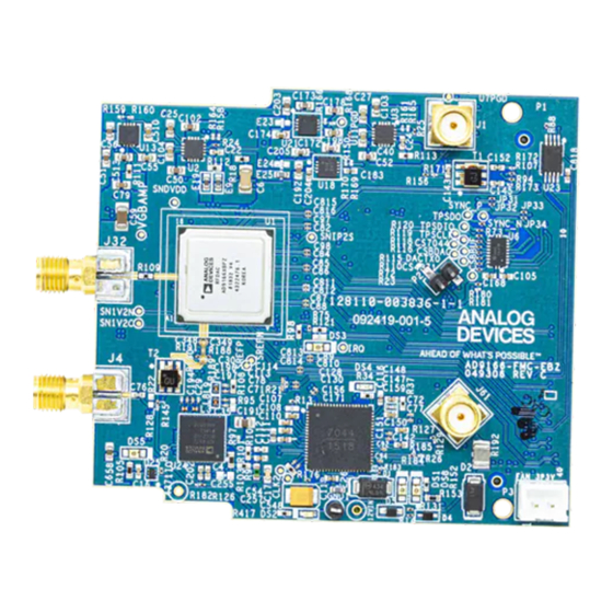
AD9166-FMC-EBZ EVALUATION BOARD PHOTOGRAPH
Rev. 0 | Page 1 of 23
AD9166-FMC-EBZ
DC to 9 GHz Vector Signal Generator
array (FPGA) mezzanine card (FMC) power supply provided
through the ADS7-V2EBZ.
Figure 1 shows the top side of the evaluation board. The
evaluation board includes a clock buffer, the HMC7044, which
provides a reference clock to the
signals to both the
ADS7-V2EBZ
converter (DAC) integrated inside the AD9166. The on-board
ADF4372
generates a sampling clock for the DAC.
The reference and sampling clocks can be connected externally
through the on-board Subminiature Version A (SMA) ports.
SYSREF± can be connected from an external source, such as an
FPGA development kit, across the FMC connector to the
AD9166.
The various clock configurations are outlined in Figure 3. The
clock paths can be selected by soldering 0 Ω resistors (jumpers)
in the correct locations on the evaluation board and configuring
the
ADF4372
and
HMC7044
Clocking section.
Complete specifications for the
AD9166
data sheet available from Analog Devices, Inc., and
must be consulted in conjunction with this user guide when
using the evaluation board.
Figure 1.
User Guide
UG-1698
ADS7-V2EBZ
and SYSREF±
and the digital-to-analog
as described in the On-Board
AD9166
can be found in the
Advertisement
Table of Contents

Related Manuals for Analog Devices AD9166-FMC-EBZ


Summary of Contents for Analog Devices AD9166-FMC-EBZ
-
Page 1: Features
The various clock configurations are outlined in Figure 3. The clock paths can be selected by soldering 0 Ω resistors (jumpers) GENERAL DESCRIPTION in the correct locations on the evaluation board and configuring This user guide is for the AD9166-FMC-EBZ evaluation board. ADF4372 HMC7044 as described in the On-Board... -
Page 2: Table Of Contents
General Description ................. 1 Using the ADS7-V2EBZ to Play a Pattern to the Evaluation Board ....................11 AD9166-FMC-EBZ Evaluation Board Photograph ..... 1 Configure the Spectrum Analyzer ........... 11 Revision History ................2 Load and Play Pattern to the ADS7-V2EBZ ......11 Evaluation Board Hardware ............ -
Page 3: Evaluation Board Hardware
FIN, the external VCO input on the CLKIN1/FIN pin of the HMC7044, and bypass PLL2 altogether. Using the CLKIN1/FIN A block diagram of the clock paths on the AD9166-FMC-EBZ pin is the default clocking scheme on the AD9166-FMC-EBZ evaluation board is shown in Figure 3. -
Page 4: External Clocking
1. ALL SWITCHES ARE 0Ω RESISTORS (SOLDER JUMPERS). 2. REF IS THE REFERENCE INPUT. 3. FIN IS THE EXTERNAL VCO INPUT ON THE CLKIN1/FIN PIN. Figure 3. Block Diagram of the AD9166-FMC-EBZ Evaluation Board Rev. 0 | Page 4 of 23... -
Page 5: Evaluation Board Software
AD9166-FMC-EBZ User Guide UG-1698 EVALUATION BOARD SOFTWARE The AD9166-FMC-EBZ evaluation board is configured using Use the DPGDownloader program for loading signal vectors an easy to use graphical user interface called analysis, control, into the ADS7-V2EBZ, to be played by the... -
Page 6: Hardware Setup
JESD204B link to supply data samples from an FPGA. Consider using an FMC adapter to avoid wearing out the FMC AD9166 operates as a direct digital synthesizer (DDS). connector. However, the SPI bus to control the AD9166-FMC-EBZ is Rev. 0 | Page 6 of 23... -
Page 7: Getting Started
INITIAL SETUP DPGDownloader software and the necessary files for the Complete the following initial steps to get started with the AD9166-FMC-EBZ evaluation board, including the schematic, evaluation of the device: board layout, and data sheet. Download the DPGDownloader Install the DPGDownloader software on the PC. Analog... -
Page 8: Dc Test/Nco Mode
1 GHz: For Operation Mode, select DC Test Mode. Ensure that the AD9166-FMC-EBZ evaluation board is Set FDAC to 4.9152 GHz. configured and powered up according to the Hardware Select the NCO Enable box. - Page 9 AD9166-FMC-EBZ User Guide UG-1698 Figure 6. ACE—Initial Configuration Figure 7. AD9166 Chip View and Clock Source Selection in Rev. 0 | Page 9 of 23...
- Page 10 UG-1698 AD9166-FMC-EBZ User Guide Figure 8. Spectrum Analyzer Plot of DAC Output in NCO Mode (Showing a Single Tone at 1 GHz) Rev. 0 | Page 10 of 23...
-
Page 11: Using The Ads7-V2Ebz To Play A Pattern To The Evaluation Board
AD9166-FMC-EBZ User Guide UG-1698 USING THE ADS7-V2EBZ TO PLAY A PATTERN TO THE EVALUATION BOARD CONFIGURE THE SPECTRUM ANALYZER LOAD AND PLAY PATTERN TO THE ADS7-V2EBZ Configure the spectrum analyzer as follows: Configure the hardware according to the instructions provided in the Hardware Setup section. - Page 12 Status indicator may show a red cross, as shown in Figure 11. the data-words to create 16-bit words for transfer to the 13. Click the download button to download the pattern from data framer. Because the datapath is 16 bits, Analog Devices the computer to the ADS7-V2EBZ unit.
-
Page 13: Configure The Evaluation Board
The minimum interpolation ratio is 1 for the AD9166. Click the Apply button at the bottom of the AD9166 STARTUP WIZARD window. Figure 12. AD9166-FMC-EBZ Evaluation Board View and Clock Source Selection in Rev. 0 | Page 13 of 23... - Page 14 UG-1698 AD9166-FMC-EBZ User Guide Note the line rate frequency from the AD9166 in the Set the Frequency Shift field to the desired shift frequency DPGDownloader window as 6.75 Gbps, as shown in (in Hz). Figure 15. The SYNC Status indicator then changes to the Change the DC Back-Off(dB) box to 0 dB.
- Page 15 AD9166-FMC-EBZ User Guide UG-1698 Generate and download other vectors after the JESD204B Figure 15. The data type is real only (not complex) and link is up. Interpolation Mode is set to 1X. 10. Repeat Step 2 to Step 6 to run a new setting, such as a...
-
Page 16: Using External Files
UG-1698 AD9166-FMC-EBZ User Guide USING EXTERNAL FILES ADF4372 phase frequency detector (PFD) spur level is related to the PFD frequency. A lower PFD frequency can help The DPGDownloader software allows users to import and use reduce the PFD spur, while it also narrows the loop bandwidth files generated outside the tool. -
Page 17: Ace User Guide
AD9166-FMC-EBZ User Guide UG-1698 USER GUIDE views can program the registers and are based on user preference. A comprehensive user guide is available on the Analog Devices, Inc., website. For any general information relating to Because the AD9166 has a large register map, the Functional... -
Page 18: Jesd204B Lane Mapping Of The Ad9166-Fmc-Ebz Evaluation Board
AD9166 (Lane 4 of the Xilinx JESD204B IP) The user can configure another Xilinx Virtex7-based evaluation board to drive the AD9166-FMC-EBZ evaluation board. The There is also input data pin polarity (positive and negative) JESD204B parameters are available in the AD9166 data sheet. -
Page 19: Troubleshooting
DPGDownloader Does Not Recognize the Evaluation Board Debugging the Evaluation Board Using On-Board LEDs The AD9166-FMC-EBZ evaluation board can be run with or There are six LEDs on the AD9166-FMC-EBZ evaluation board: without an ADS7-V2EBZ, as long as it is connected across the DS1, DS2, DS3, DS4, DS5, and DS8. - Page 20 (SERDES) link does not come up: Before configuring the AD9166-FMC-EBZ evaluation board, it Check to ensure that the DPGDownloader software is is a good practice to soft reset the evaluation board by clicking configured to play a particular signal vector (sometimes...
- Page 21 AD9166-FMC-EBZ User Guide UG-1698 Figure 22. Register Write Error Indicating Does Not Recognize the Evaluation Board Rev. 0 | Page 21 of 23...
- Page 22 UG-1698 AD9166-FMC-EBZ User Guide ADS7-V2EBZ Firmware Update Needed To manually update the ADS7-V2EBZ firmware, open the DPGDownloader application and click the Advanced/Debug Each ADS7-V2EBZ is loaded with the latest firmware available button, as shown in Figure 23. Click the Update button. The at the time of manufacturing.
- Page 23 By using the evaluation board discussed herein (together with any tools, components documentation or support materials, the “Evaluation Board”), you are agreeing to be bound by the terms and conditions set forth below (“Agreement”) unless you have purchased the Evaluation Board, in which case the Analog Devices Standard Terms and Conditions of Sale shall govern. Do not use the Evaluation Board until you have read and agreed to the Agreement.
Need help?
Do you have a question about the AD9166-FMC-EBZ and is the answer not in the manual?
Questions and answers