Advertisement
Quick Links
One Technology Way • P.O. Box 9106 • Norwood, MA 02062-9106, U.S.A. • Tel: 781.329.4700 • Fax: 781.461.3113 •
Getting Started with the AD9125-EBZ Evaluation Board
WHAT'S IN THE BOX
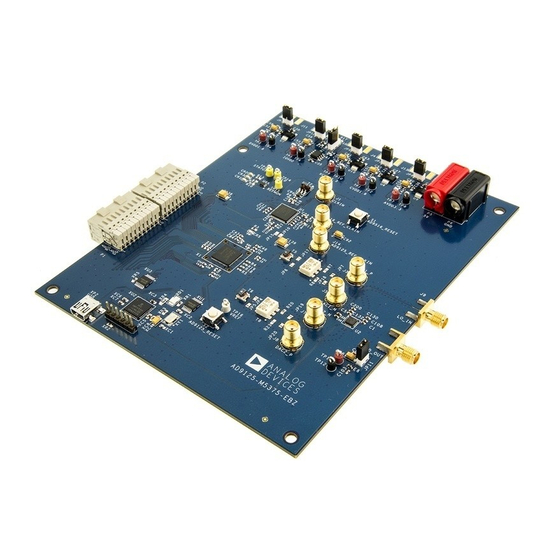
AD9125-EBZ Evaluation Board
Evaluation Board CD
Mini-USB Cable
INTRODUCTION
The AD9125 Evaluation Board connects to the Analog Devices Digital Pattern Generator (DPG) to allow for quick evaluation of the
AD9125. Control of the SPI port in the AD9125 is available through USB with accompanying PC software.
To ease the subsystem evaluation, a clock distribution chip (AD9516) and a quadrature modulator are also designed into this evaluation
board.
SOFTWARE
The AD9125 Evaluation Board is designed to receive data from a Data Patten Generator (DPG). The DAC Software Suite, plus the AD9125
Update, is required for evaluation. The DAC Software Suite is included on the Evaluation Board CD, or can be downloaded from the DPG
web site at http://www.analog.com/dpg. This will install DPGDownloader (for loading vectors into the DPG) and the AD9125 SPI
Controller application. The AD9125 Evaluation Board DPGDownloader software has an easy-to-use legacy graphical user interface (GUI),
but ACE, a newer evaluation software from ADI, is the preferred evaluation software. ACE can be downloaded from the ACE website at
https://wiki.analog.com/resources/tools-software/ace. The ACE plug-in for the evaluation board is available for download on the AD9125
eval webpage in the software section at http://www.analog.com/en/design-center/evaluation-hardware-and-software/evaluation-boards-
kits/EVAL-AD9125.html#eb-overview.
HARDWARE SETUP
Connect a +5V DC power supply to the banana jacks (P5 and P6). A clock source should be connected to the SMA jack labeled J1 (CLKIN)
and should be set to 500 MHz and 3 dBm. A second clock source should be connected to the SMA jack labeled J9 (LO_IN). This source
should be set to 1.8 GHz and 0 dBm. The AD9516 buffers this clock and distributes clock signals with proper frequencies to the AD9125
and the DPG. In order to monitor the AD9125 outputs, a spectrum analyzer should be connected to the SMA jack labeled J3 (DAC1_P) for
I channel DAC, J8 (DAC2_P) for Q channel DAC, or J6 (MOD_OUT) for the quadrature modulator output. The DPG connects through
connector P1 and P2 on the left edge of the evaluation board, and the USB cable should be connected to the mini USB connector labeled
XP2 USB on the lower left side of the board. Note that the PC software needs to be installed before connecting the USB cable to your
computer.
Information furnished by Analog Devices is believed to be accurate and reliable. However, no
responsibility is assumed by Analog Devices for its use, nor for any infringements of patents or other
rights of third parties that may result from its use. Specifications subject to change without notice.
No license is granted by implication or otherwise under any patent or patent rights of Analog
Devices. Trademarks and registered trademarks are the property of their respective owners.
AD9125 Evaluation Board
www.analog.com
RECOMMENDED EQUIPMENT
Sinusoidal Clock Source (at least 1.0 GHz)
Sinusoidal Clock Source (for modulator LO)
Spectrum Analyzer
DC Power Supply
Digital Pattern Generator Series 2 or 3 (DPG)
One Technology Way, P.O. Box 9106, Norwood, MA 02062-9106, U.S.A.
Tel: 781.329.4700
Fax: 781.461.3113
Quick Start Guide
www.analog.com
©2010 Analog Devices, Inc. All rights reserved.
Advertisement

Related Manuals for Analog Devices AD9125


Summary of Contents for Analog Devices AD9125
- Page 1 500 MHz and 3 dBm. A second clock source should be connected to the SMA jack labeled J9 (LO_IN). This source should be set to 1.8 GHz and 0 dBm. The AD9516 buffers this clock and distributes clock signals with proper frequencies to the AD9125 and the DPG.
-
Page 2: Jumper Configurations
Figure 2: Modulator Output Configuration The solder jumper on the left side of C139 determines whether the ref/sync clock of the AD9125 is from the AD9516 or an external source through the SMA jack J14 (AD9125_REF_CLKIN). When the AD9516 is used for the clock source, the jumper should be configured so that the center pad is connected to the top pad. - Page 3 If the board is connected properly, ACE will detect it and display it on the Start page under “Attached Hardware. ” Double click this board. Ensure that the button is green in the subsystem image under the “System” tab. If not, click it, select the AD9125, and click “Acquire. ” Double click on the subsystem image.
- Page 4 Quick Start Guide AD9125-EBZ Figure 6 Double click on the dark blue AD9125 on the board diagram. Ensure that the settings of the AD9125 match with Figure 7 and click “Apply Changes. ” Figure 7 Open the DPG Downloader software. The ‘DCO frequency’ shown should be 250MHz. (Due to the resolution of the DPG frequency counter, the measured frequency could be a little off).
- Page 5 SPI Software This setup configures the AD9125 to generate a sine wave by using the DPG as a data source. This allows the user to measure the singletone AC performance at the DAC output. Install the software as described in the Software section, and connect all the required cables as described in the Hardware Setup section.
- Page 6 Using the DAC output jumper configuration, along with the same ACE and DPGDownloader setups, the resulting spectrum out of J3 is in Figure __ and the resulting spectrum of J8 is in Figure __. ©2010 Analog Devices, Inc. All rights reserved. Trademarks and registered trademarks are the property of their respective owners.
-
Page 7: Appendix A: Spi Controller
DAC receives data first from the interleaved bus. For use with the DPG2, this should always be set to IQ Pairs. The Interface Mode selects how wide the data bus will be. This setting will need to match the setting in the DPG AD9125 panel for proper operation with the DPG2. -
Page 8: Appendix B - Ace Software Features
Main DAC Control This tab controls the two main DACs in the AD9122/AD9125. The Full-Scale Current of each DAC can be set with the I DAC Gain and Q DAC Gain controls. The I Sleep and Q Sleep controls put their respective DAC into a low-power sleep state. When the AD9122/AD9125 is used with a modulator, the Phase Compensation/DC Offset controls can be used to correct any mismatches between the two DACs. - Page 9 More direct changes to registers and bit fields can be made in the memory map, which is linked from the chip block diagram (Figure 7) through the “Proceed to Memory Map” button. In this view, names, addresses, and data can be manually altered by the user. ©2010 Analog Devices, Inc. All rights reserved. Trademarks and registered trademarks are the property of their respective owners.
- Page 10 Figure 67: Macro tool in ACE. The “Stop Recording,” “Record,” and “Save Macro” commands are located at the top of the macro tool ©2010 Analog Devices, Inc. All rights reserved. Trademarks and registered trademarks are the property of their respective owners.
- Page 11 Figure 78: Conversion set-up for macro to hex Figure 19: Converted text file For more information about ACE and its features, visit https://wiki.analog.com/resources/tools-software/ace. ©2010 Analog Devices, Inc. All rights reserved. Trademarks and registered trademarks are the property of their respective owners. D00000-0-1/07(A)
Need help?
Do you have a question about the AD9125 and is the answer not in the manual?
Questions and answers