
Subscribe to Our Youtube Channel
Related Manuals for Cypress CY14NVSRAMKIT-001


Summary of Contents for Cypress CY14NVSRAMKIT-001
- Page 1 CY14NVSRAMKIT-001 nvSRAM Development Kit User Guide Doc. # 002-03522 Rev. *A Cypress Semiconductor 198 Champion Court San Jose, CA 95134-1709 www.cypress.com...
- Page 2 Cypress is not liable, in whole or in part, and you shall and hereby do release Cypress from any claim, damage, or other liability arising from or related to all Unintended Uses of Cypress products.
-
Page 3: Table Of Contents
6. Kit Example Firmware Example Firmware Structure ..................41 nvSRAM Access APIs ....................42 6.2.1 nvSRAMRead (uint32_t address, uint8_t length, uint8_t *txData) ....42 6.2.2 void nvSRAMWrite (uint32_t address, uint16_t data) ........43 CY14NVSRAMKIT-001 nvSRAM Development Kit User Guide, Doc. # 002-03522 Rev. *A... - Page 4 CY14NVSRAMKIT-001 Kit Block Diagram ..............49 CY14NVSRAMKIT-001 Kit Components Placement ..........50 CY14NVSRAMKIT-001 Kit Schematic...............51 Pin Assignment Table ....................55 Bill of Materials (BOM) ....................58 FM4 MCU Evaluation Board ..................61 Revision History CY14NVSRAMKIT-001 nvSRAM Development Kit User Guide, Doc. # 002-03522 Rev. *A...
-
Page 5: Safety Information
If such interference is detected, suitable mitigating measures should be taken. The CY14NVSRAMKIT-001, as shipped from the factory, has been verified to meet with the requirements of CE as a Class A product. - Page 6 Handling Supercapacitors The CY14NVSRAMKIT-001 board uses a 0.1 Farad supercapacitor for RTC backup. It is advisable not to touch the capacitor positive pin (anode) with a bare hand or a conducting material to avoid electrical shock.
-
Page 7: Introduction
Introduction Thank you for your interest in the CY14NVSRAMKIT-001 nvSRAM Development Kit (DVK). The kit (shield) is designed as an easy-to-use and inexpensive development kit, showcasing the features of Cypress high-speed, parallel access (asynchronous interface), nonvolatile SRAM (nvSRAM). This kit works in conjunction with the SK-FM4-U120-9B560 FM4 MCU Evaluation Board, a starter kit for ®... -
Page 8: Getting Started
Visit www.cypress.com/CY14NVSRAMKIT-001 for more information. Inspect the contents of the kit; if you find any part missing, contact your nearest Cypress sales office for help. Getting Started This guide helps you to get acquainted with the CY14NVSRAMKIT-001 DVK. The Kit Installation chapter on page 10 describes the installation of the kit software. -
Page 9: Additional Learning Resources
FBGA fine-pitch ball grid array microcontroller unit nvSRAM nonvolatile static random access memory quick start guide real time clock TSOP thin small outline package user guide CY14NVSRAMKIT-001 nvSRAM Development Kit User Guide, Doc. # 002-03522 Rev. *A... -
Page 10: Kit Installation
Therefore, all software and drivers for that evaluation board need to be installed to work with the CY14NVSRAMKIT-001 DVK. Follow these steps to install the FM4-related software and drivers. 1. Download the “Complete Driver, Documentation, Software and Tools package” from the... -
Page 11: Uninstall Sk-Fm4-U120-9B560 Kit Software And Driver
(see Figure 2-4). Figure 2-4. nvSRAM DVK Software The CY14NVSRAMKIT-001 Kit Setup executable file installs the kit contents, which include kit software, firmware, hardware files, and user documents. 2. The kit startup screen appears as shown in Figure 2-5. - Page 12 When the installation begins, a list of packages appears on the installation page. A green check mark appears next to each package after successful installation. 4. If this is the first Cypress product that you have installed, enter your contact information or select Continue without Contact Information. Click Finish to complete the kit installation.
-
Page 13: Uninstall Cy14Nvsramkit-001 Dvk Contents
Go to Start > Control Panel > Programs and Features; select the appropriate software ■ package and click Uninstall. Go to Start > All Programs > Cypress > Cypress Update Manager > Cypress Update ■ Manager. Select the CY14NVSRAMKIT-001 Kit Rev ** row and click Uninstall. -
Page 14: Kit Overview
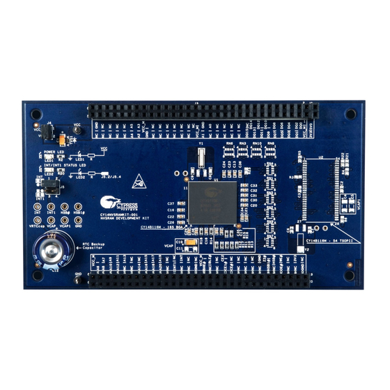
Kit Overview CY14NVSRAMKIT-001 Kit Overview The CY14NVSRAMKIT-001 DVK can be used to understand the features of parallel nvSRAMs (asynchronous interface). The DVK is an add-on board, which contains a 16-Mbit, x16, 3.3 V, parallel nvSRAM with RTC. It provides two 30x2 headers (J1 and J3) compatible with an SK-FM4-U120- 9B560 FM4 MCU Evaluation Board. -
Page 15: Kit Introduction And Configuration Guide
The following sections describe various aspects of the kit hardware and the kit setup. 3.2.1 Power Supply Jumper The CY14NVSRAMKIT-001 DVK hardware operates at 3.3 V, selected through header J4, as shown Figure 3-2. The factory default jumper setting is 3.3 V (short pins 1 and 2 of J4). -
Page 16: Interrupt (Int And Int1) Pins
INT/INT1 STATUS LED can cause output contention when the output driver of either nvSRAM is configured as active HIGH (push or pull) output. CY14NVSRAMKIT-001 nvSRAM Development Kit User Guide, Doc. # 002-03522 Rev. *A... -
Page 17: Test Points
Test point for the kit board ground CAUTION: The VCC test point is only for probing and measurement purposes. Do not power the kit using this test point to avoid any damage to the board. CY14NVSRAMKIT-001 nvSRAM Development Kit User Guide, Doc. # 002-03522 Rev. *A... -
Page 18: 54 Tsop Ii - Not Populated By Default
Figure 3-8. FM4 MCU Evaluation Board Mounted on CY14NVSRAMKIT-001 CAUTION: The FM4 MCU Evaluation Board is plugged onto the CY14NVSRAMKIT-001 DVK through its compatible headers J1, J2, and J3. Because J1 and J3 are high pin-count connectors on the FM4 MCU Eval- uation Board, removing the FM4 MCU Evaluation Board can be difficult and may lead to bending its J1 and J3 connector pins. - Page 19 Kit Overview Figure 3-9. 3.3-V Setting on FM4 MCU Evaluation Board CY14NVSRAMKIT-001 nvSRAM Development Kit User Guide, Doc. # 002-03522 Rev. *A...
-
Page 20: Kit Operation
The FM4 MCU is a 32-bit ARM Cortex-M4 microcontroller device. A firmware code is required to configure the MCU as the nvSRAM host controller to access the nvSRAM device on the CY14NVSRAMKIT-001 DVK. The firmware example code provided with the DVK collateral supports different nvSRAM functionalities such as write/read memory access, RTC register access, hardware store, software store, and sleep mode by toggling the dedicated sleep (ZZ#) pin on the nvSRAM. - Page 21 Note: LED5 (Green) indicates the board is powered from the USB port via the CN3 connector. LED3 (Red) indicates the board is powered in the Programming (and Debugging) mode. CY14NVSRAMKIT-001 connection to the FM4 MCU Evaluation Board is not necessary during programming.
- Page 22 Debug and Programming (DAP) port (CN3) driver. 9. Click the Full Operation button to program the device. When the operation starts, a window pops up with the message shown in Figure 4-6. CY14NVSRAMKIT-001 nvSRAM Development Kit User Guide, Doc. # 002-03522 Rev. *A...
- Page 23 Figure 4-7. End of MCU Flash Programming 11. After the programming is complete, the other buttons, which were grayed out initially, are enabled. However, these operations are not required to use the nvSRAM DVK. CY14NVSRAMKIT-001 nvSRAM Development Kit User Guide, Doc. # 002-03522 Rev. *A...
-
Page 24: Run The Fm4 Mcu Evaluation Board
7. Connect the MCU board to a PC via the CN4 port. Refer to A.6.5 Jumper Setting Table - FM4 MCU Evaluation Board Run Mode on page 64 more details. CY14NVSRAMKIT-001 nvSRAM Development Kit User Guide, Doc. # 002-03522 Rev. *A... - Page 25 Spansion Virtual Communications Port driver. Connecting the FM4 MCU Evaluation Board USB port ‘CN4’ to the PC should recognize the port as a ‘Spansion Virtual Communications Port’. CY14NVSRAMKIT-001 nvSRAM Development Kit User Guide, Doc. # 002-03522 Rev. *A...
-
Page 26: Spansion Virtual Communication Port Driver Installation
Ports (COM & LPT) in the Device Manager as shown in Figure 4-18. 4. If the driver is not installed, the board appears as Virtual Comm Port under Other devices in the Device Manager as shown in Figure 4-13. CY14NVSRAMKIT-001 nvSRAM Development Kit User Guide, Doc. # 002-03522 Rev. *A... - Page 27 Figure 4-13. Other Devices - Virtual Comm Port 5. Right-click Virtual Comm Port and select Properties as shown in Figure 4-14. The Virtual Comm Port Properties window opens up; select Update Driver from the Driver tab. CY14NVSRAMKIT-001 nvSRAM Development Kit User Guide, Doc. # 002-03522 Rev. *A...
- Page 28 Figure 4-14. Update Virtual Comm Port Driver 6. In the Update Driver window, select Browse my computer for driver software as shown in Figure 4-15. Figure 4-15. Browse Virtual Comm Port Driver Software CY14NVSRAMKIT-001 nvSRAM Development Kit User Guide, Doc. # 002-03522 Rev. *A...
- Page 29 9. When the driver is installed successfully, the board will appear as Spansion Virtual Communi- cations Port under Ports (COM & LPT) in the Device Manager as shown in Figure 4-18. Now the board is ready for use with the CY14NVSRAMKIT-001 DVK software. CY14NVSRAMKIT-001 nvSRAM Development Kit User Guide, Doc. # 002-03522 Rev. *A...
-
Page 30: Development Kit Setup
CAUTION: Remove the USB connection to power off the FM4 MCU Evaluation Board before plugging on the CY14NVSRAMKIT-001 board. Software details are provided in the Kit Software chapter on page CY14NVSRAMKIT-001 nvSRAM Development Kit User Guide, Doc. # 002-03522 Rev. *A... - Page 31 Note: The CY14NVSRAMKIT-001 DVK factory setting is 1 Hz square-wave output at the INT pin. This will blink the INT/INT1 STATUS LED (LED2) every second when the jumper J5 pin 1 and 2 is shorted with 3.3 V VCC power applied to the kit.
-
Page 32: Kit Software
Kit Software Open the nvSRAM kit software from Start > All Programs > Cypress > nvSRAM Kit. Figure 5-1. nvSRAM Kit Software Startup Window CY14NVSRAMKIT-001 nvSRAM Development Kit User Guide, Doc. # 002-03522 Rev. *A... - Page 33 The kit will appear as "Spansion Virtual Communications Port". Select this COM port from the drop- down list. When the COM port is selected, the COM port status will change to CONENCTED as indi- cated in Figure 5-2. Figure 5-2. nvSRAM Features CY14NVSRAMKIT-001 nvSRAM Development Kit User Guide, Doc. # 002-03522 Rev. *A...
- Page 34 - Sleep: Drives nvSRAM ZZ# low and puts it in the SLEEP mode. - Wakeup: Drives nvSRAM ZZ# high and wakes it up from the SLEEP mode. Execute Clicking this button will execute the selected nvSRAM feature. CY14NVSRAMKIT-001 nvSRAM Development Kit User Guide, Doc. # 002-03522 Rev. *A...
- Page 35 Clicking this button will read from the selected RTC registers. A read operation will set the Read 'R' bit automatically for the RTC reading except the Flags register. CY14NVSRAMKIT-001 nvSRAM Development Kit User Guide, Doc. # 002-03522 Rev. *A...
- Page 36 Set squarewave 512 Hz 4096 Hz 32768 Hz Note: After setting squarewave, the nvSRAM RTC registers are read back and the GUI is updated with data from the device. CY14NVSRAMKIT-001 nvSRAM Development Kit User Guide, Doc. # 002-03522 Rev. *A...
- Page 37 Kit Software The File menu functions are shown in Figure 5-4. Figure 5-4. Load/Dump Features Figure 5-5. Load Memory Figure 5-6. Dump Memory Figure 5-7. Load RTC Selection CY14NVSRAMKIT-001 nvSRAM Development Kit User Guide, Doc. # 002-03522 Rev. *A...
- Page 38 Kit Software Figure 5-8. Load RTC Figure 5-9. Dump RTC Selection CY14NVSRAMKIT-001 nvSRAM Development Kit User Guide, Doc. # 002-03522 Rev. *A...
- Page 39 This menu selection will dump the 16 bytes of data from the nvSRAM RTC registers to a Dump RTC… file. Exit This menu selection will exit the application. The Help menu functions are shown in Figure 5-11. CY14NVSRAMKIT-001 nvSRAM Development Kit User Guide, Doc. # 002-03522 Rev. *A...
- Page 40 Table 5-4. Help Menu Help Menu Description User Guide… This menu selection (or pressing [F1]) will open the kit user guide. About… This menu selection provides information about the nvSRAM Kit Software CY14NVSRAMKIT-001 nvSRAM Development Kit User Guide, Doc. # 002-03522 Rev. *A...
-
Page 41: Kit Example Firmware
Project Files File Path <Install_Directory>\CY14NVSRAMKIT-001 nvSRAM Development Main project Kit\1.0\Firmware\Source\main_project\IAR <Install_Directory>\CY14NVSRAMKIT-001 nvSRAM Development nvSRAM project files Kit\1.0\Firmware\Source\cypress\nvp\nvSRAM\ <Install_Directory>\CY14NVSRAMKIT-001 nvSRAM Development FM4 library Kit\1.0\Firmware\Source\library <Install_Directory>\CY14NVSRAMKIT-001 nvSRAM Development Bin file Kit\1.0\Firmware\Source\main_project\IAR\nvSRAM_Kit\Exe CY14NVSRAMKIT-001 nvSRAM Development Kit User Guide, Doc. # 002-03522 Rev. *A... -
Page 42: Nvsram Access Apis
(uint32_t address, uint8_t length, uint8_t *txData) /****************************************************************************** ** \param address - memory address ** \param length - number of bytes to read ** \param txData - read data buffer CY14NVSRAMKIT-001 nvSRAM Development Kit User Guide, Doc. # 002-03522 Rev. *A... -
Page 43: Void Nvsramwrite (Uint32_T Address, Uint16_T Data)
** \param length - number of bytes to read ** \param txData - read data buffer *****************************************************************************/ void nvSRAMReadRTC (uint8_t address, uint8_t length, uint8_t *txData) uint16_t tempData; uint8_t u8Counter; CY14NVSRAMKIT-001 nvSRAM Development Kit User Guide, Doc. # 002-03522 Rev. *A... -
Page 44: Void Nvsramwritertc (Uint8_T Address, Uint8_T Data)
** \param pat - user data pattern type (0x01, 0x02, 0x03, 0x04) ** \param data - write data word *****************************************************************************/ void write_data_pattern (uint8_t pat, uint16_t data) switch(pat) case DATA_PAT: \\ pat = 0x00 nvSRAMWriteFullMem(data, data); break; CY14NVSRAMKIT-001 nvSRAM Development Kit User Guide, Doc. # 002-03522 Rev. *A... -
Page 45: Void Autostore (Boolean_T Enable)
(FUNCTION_MODE_2, 0x1, temp); \\ FUNCTION_MODE_2 is read address 0x83E0 nvSRAMRead (FUNCTION_MODE_3, 0x1, temp); \\ FUNCTION_MODE_3 is read address 0x7C1F nvSRAMRead (FUNCTION_MODE_4, 0x1, temp); \\ FUNCTION_MODE_4 is read address 0x703F CY14NVSRAMKIT-001 nvSRAM Development Kit User Guide, Doc. # 002-03522 Rev. *A... -
Page 46: Void Softwarestorerecall (Boolean_T Mode)
(M_SOFTRECALL_ENABLE, 0x1, temp); \\ M_ SOFTRECALL_ENABLE is read address 0x4C63 6.2.10 void SleepIF (boolean_t mode) /******************************************************************************** ** \param mode - true, enables nvSRAM sleep; false, disables nvSRAM sleep CY14NVSRAMKIT-001 nvSRAM Development Kit User Guide, Doc. # 002-03522 Rev. *A... -
Page 47: Void Squarewave (Uint8_T Mode)
This section describes changes to be made in the firmware to enable access for the 16-Mbit, 1Mx16 nvSRAM (CY14B116M) in the 54 TSOP II package. This package option is default DNI on the CY14NVSRAMKIT-001 DVK hardware. The hardware must be populated with the CY14B116M, 54 TSOP II nvSRAM to access this feature. -
Page 48: Changes In Cy14B116.H
The sleep pin (ZZ#) is not available on the nvSRAM 54 TSOP II package. Hence, the Sleep and Wakeup features, described in Table 5-1 on page 34, is not applicable for the 54 TSOP II package. CY14NVSRAMKIT-001 nvSRAM Development Kit User Guide, Doc. # 002-03522 Rev. *A... -
Page 49: Appendix
Appendix CY14NVSRAMKIT-001 Kit Block Diagram CY14NVSRAMKIT-001 nvSRAM Development Kit User Guide, Doc. # 002-03522 Rev. *A... -
Page 50: Cy14Nvsramkit-001 Kit Components Placement
CY14NVSRAMKIT-001 Kit Components Placement CY14NVSRAMKIT-001 nvSRAM Development Kit User Guide, Doc. # 002-03522 Rev. *A... -
Page 51: Cy14Nvsramkit-001 Kit Schematic
CY14NVSRAMKIT-001 Kit Schematic CY14NVSRAMKIT-001 nvSRAM Development Kit User Guide, Doc. # 002-03522 Rev. *A... - Page 52 CY14NVSRAMKIT-001 nvSRAM Development Kit User Guide, Doc. # 002-03522 Rev. *A...
- Page 53 CY14NVSRAMKIT-001 nvSRAM Development Kit User Guide, Doc. # 002-03522 Rev. *A...
- Page 54 CY14NVSRAMKIT-001 nvSRAM Development Kit User Guide, Doc. # 002-03522 Rev. *A...
-
Page 55: Pin Assignment Table
Port 5_9 MADATA10_0 Port 5_A MADATA11_0 Port 5_B MADATA12_0 Port 3_0 MADATA13_0 Port 3_1 MADATA14_0 Port 3_2 MADATA15_0 Port 3_3 MAD00_0 Port 3_D MAD01_0 Port 3_E MAD02_0 Port 3_F CY14NVSRAMKIT-001 nvSRAM Development Kit User Guide, Doc. # 002-03522 Rev. *A... - Page 56 Port 1_6 MAD14_0 Port 1_7 MAD15_0 Port 1_8 MAD16_0 Port 1_9 MAD17_0 Port 1_A MAD18_0 Port 1_B MAD19_0 Port 1_C MAD20_0 Port 1_D A20 (32 Mb) MAD21_0 Port 1_E CY14NVSRAMKIT-001 nvSRAM Development Kit User Guide, Doc. # 002-03522 Rev. *A...
- Page 57 MCSX4_0 Port 0_8 CE# (54-TSOP II) MCSX3_0 Port 0_6 Port 6_7 HSB1# (54-TSOP) 110 Port 6_6 HSB# (165-FBGA) 111 Port 6_5 Port 6_4 MWEX_0 Port 6_3 MOEX_0 Port 6_2 CY14NVSRAMKIT-001 nvSRAM Development Kit User Guide, Doc. # 002-03522 Rev. *A...
-
Page 58: Bill Of Materials (Bom)
CMD17-21VGC/TR8 0805 SMD Visual Communica- LED RED CLEAR 0805 LED2 LED Red tions Company - CMD17-21VRC/TR8 RES SMD 330 OHM 1% Panasonic Elec- 330E ERJ-3EKF3300V 1/10W 0603 tronic Components CY14NVSRAMKIT-001 nvSRAM Development Kit User Guide, Doc. # 002-03522 Rev. *A... - Page 59 TP14 VRTCcap_TP 5001 .040"D Black Crystal 32.7680kHz 20ppm 12.5pF 50 kOhm - 32.768 KHz Citizen Finedevice CMR200T32.768KDZF 40°C - 85°C Surface (12.5 pF) Co Ltd Mount Cylindrical Can, Radial CY14NVSRAMKIT-001 nvSRAM Development Kit User Guide, Doc. # 002-03522 Rev. *A...
- Page 60 "Cypress Semicon- 2", "Attention Observe ductor Precautions Install on Bottom of PCB As per the Silk Screen in the Corners BUMPER CYLINDRI- Bumpon Protective SJ61A6 CAL .312X.215 BLACK Products Rollstock CY14NVSRAMKIT-001 nvSRAM Development Kit User Guide, Doc. # 002-03522 Rev. *A...
-
Page 61: Fm4 Mcu Evaluation Board
This section provides details on the SK-FM4-U120-9B560 FM4 MCU Evaluation Board jumpers and their settings in Program and Run modes. A.6.1 FM4 MCU Evaluation Hardware (Top Side) - Jumper Details A.6.2 FM4 MCU Evaluation Hardware (Top Side) - Jumper Function Overview CY14NVSRAMKIT-001 nvSRAM Development Kit User Guide, Doc. # 002-03522 Rev. *A... - Page 62 (Do not change!) Closed: Test-Mode Open: Run-Mode Operation of MD0 Closed: Programming-Mode Open: SIN0 is disconnected from CMSIS-DAP CMSIS-DAP Closed: CMSIS-DAP’s virtual COM port is Virtual COM port (SIN0_0) connect CY14NVSRAMKIT-001 nvSRAM Development Kit User Guide, Doc. # 002-03522 Rev. *A...
- Page 63 Sets Mode 1 pin (MD1) for programming J1-J6, J8, J9, J13, These jumpers are not populated by default (Open) on the Table A-1 J16, J17, J22-J25 FM4 MCU Evaluation Board CY14NVSRAMKIT-001 nvSRAM Development Kit User Guide, Doc. # 002-03522 Rev. *A...
- Page 64 COM port Sets jumper for blue LED (LED2) J1-J8, J13, J16, J17, These jumpers are not populated by default (Open) on the FM4 MCU Table A-1 J22-J25 Evaluation Board CY14NVSRAMKIT-001 nvSRAM Development Kit User Guide, Doc. # 002-03522 Rev. *A...
-
Page 65: Revision History
Document Title: CY14NVSRAMKIT-001 nvSRAM Development Kit User Guide Document Number: 002-03522 Origin of Revision ECN# Issue Date Description of Change Change 5052981 12/16/2015 Initial version of kit guide. 5713267 04/26/2017 SHEA Updated logo and copyright CY14NVSRAMKIT-001 nvSRAM Development Kit User Guide, Doc. # 002-03522 Rev. *A...
Need help?
Do you have a question about the CY14NVSRAMKIT-001 and is the answer not in the manual?
Questions and answers