
Related Manuals for Cypress CY15FRAMKIT-002


Summary of Contents for Cypress CY15FRAMKIT-002
- Page 1 CY15FRAMKIT-002 Serial F-RAM Development Kit User Guide Document Number: 002-23147 Rev. *A Cypress Semiconductor 198 Champion Court San Jose, CA 95134-1709 www.cypress.com...
- Page 2 Cypress product as a Critical Component in a High- Risk Device.
-
Page 3: Table Of Contents
Use of Zero-ohm and No-Load Resistors ........................30 Bill of Materials (BOM) ..............................31 CY15FRAMKIT-002 Board - Jumper Details ......................31 Appendix ................................... 33 GUI Menu ................................... 33 Revision History ................................37 CY15FRAMKIT-002 Serial F-RAM Development Kit User Guide, Document Number: 002-23147 Rev. *A... -
Page 4: Introduction
1. Introduction Thank you for your interest in the CY15FRAMKIT-002 F-RAM™ Kit (DVK). The kit (shield) is designed as an easy-to-use and inexpensive development kit as well as evaluation platform for Cypress’s latest Quad SPI enabled Serial F-RAM. This ®... -
Page 5: Kit Overview
2. Kit Overview CY15FRAMKIT-002 Kit Overview The CY15FRAMKIT-002 kit can be used to understand the features of serial F-RAMs (SPI and QSPI). The DVK is an add- ™ on board, which contains a 4-Mbit Excelon -Ultra QSPI F-RAM. It has four connectors that are Arduino UNO-compatible and connect to either an ST NUCLEO-L433RC-P MCU Evaluation Board or an Arduino UNO R3 compatible board for SPI evaluation. -
Page 6: Kit Introduction And Configuration Guide
ST NUCLEO-L433RC-P MCU Evaluation base board or other Arduino UNO R3-compatible base board. • The CY15FRAMKIT-002 board operates with 1.8 V or 3.3 V supply. Max operating voltage of the device is 3.6 V. Exceeding the maximum voltage limit (3.6 V) may damage the board. - Page 7 Morpho headers to the ST NUCLEO-L433RC-P MCU Evaluation Board for QSPI interface evaluation – Figure 4 J9 and J10. You can plug the CY15FRAMKIT-002 board onto the ST NUCLEO-L433RC-P MCU Evaluation Board through these connectors. For the schematic, see Appendix.
- Page 8 Arduino headers to the ST NUCLEO-L433RC-P MCU Evaluation Board for SPI Interface evaluation – Figure 5 J1, J2, J3 and J4. You can plug the CY15FRAMKIT-002 board onto the ST NUCLEO-L433RC-P MCU Evaluation Board through these connectors. For the schematic, see Appendix.
- Page 9 You can mount a 4-Mbit (512Kx8), Excelon-Ultra Quad SPI F-RAM device to evaluate the GQFN package in addition to the default 8-pin SOIC option on the CY15FRAMKIT-002 board. An independent chip select control is provided for the 8-pin GQFN package, which enables access to the second device on the board with an appropriate firmware modification.
-
Page 10: F-Ram And Mcu Kit Connection
Figure 9. 8-pin GQFN – Not Populated by Default 2.3 F-RAM and MCU Kit Connection The CY15FRAMKIT-002 is plugged into the ST MCU Evaluation Board through Arduino (J1, J2, J3 and J4) and Morpho (J9, J10), connectors as shown in Figure Figure 10. -
Page 11: Kit Operation
STM32L433RC controller as the target, but they can be easily modified to be compatible with any other ST microcontroller with a Quad SPI interface. In the firmware section of this document, appropriate sections will be highlighted to ensure compatibility with other ST microcontrollers. CY15FRAMKIT-002 Serial F-RAM Development Kit User Guide, Document Number: 002-23147 Rev. *A... - Page 12 The Excelon_QSPI/Inc and Excelon_QSPI/Src folders contain header files critical for initializing the QSPI and LPUART modules of the ST controller. Function declarations for accessing Cypress’s QSPI F-RAM are also provided in this folder. CY15FRAMKIT-002 Serial F-RAM Development Kit User Guide, Document Number: 002-23147 Rev. *A...
- Page 13 Before compiling, appropriate properties for the target must be selected. Press ALT+F7 or select Project > Options for Target, or click the button circled in the figure above. CY15FRAMKIT-002 Serial F-RAM Development Kit User Guide, Document Number: 002-23147 Rev. *A...
- Page 14 On the Debug tab, ST-Link Debugger should be populated automatically if the Nucleo board is plugged into a USB port on the computer and the drivers are installed correctly. Click Settings on the Debug tab to select the appropriate Flash Programming Algorithm for this device. CY15FRAMKIT-002 Serial F-RAM Development Kit User Guide, Document Number: 002-23147 Rev. *A...
- Page 15 Select the appropriate programming algorithm as shown below, and click Add. The STM32L433RC MCU has 256 KB On-Chip flash. Add the qspiFRAM.c file in the Application/User space. Add the guiFRAM.c file if you are evaluating the device features using a UART terminal. CY15FRAMKIT-002 Serial F-RAM Development Kit User Guide, Document Number: 002-23147 Rev. *A...
- Page 16 Look under Ports (COM & LPT) to determine the COM port number to use. The controller will be waiting for the appropriate GUI command. See Appendix B for GUI commands. CY15FRAMKIT-002 Serial F-RAM Development Kit User Guide, Document Number: 002-23147 Rev. *A...
-
Page 17: Quad Spi Configuration For Stm32L433Rc
FlashSize: The default value in the example project is 24, which corresponds to the total number of address bits needed to address the memory attached to the interface. The Cypress F-RAM on the kit is a 4-Mbit device but has 3-byte addressing. - Page 18 Quad SPI Interface Pin STM32L433RC Pin QUADSPI_CS# PB11 QUADSPI_CLK PB10 QUADSPI_IO0 QUADSPI_IO1 QUADSPI_IO2 QUADSPI_IO3 Figure 14. Quad SPI Pin Assignment on Morpho Connector QUADSPI_IO1 QUADSPI_CS QUADSPI_IO0 QUADSPI_IO2 QUADSPI_CLK QUADSPI_IO3 CY15FRAMKIT-002 Serial F-RAM Development Kit User Guide, Document Number: 002-23147 Rev. *A...
- Page 19 Kit Operation The CY15FRAMKIT-002 board plugs into the Nucleo board. Both Arduino and Morpho connectors need to be plugged in. In addition to initializing the Quad SPI block as described earlier, the QSPI_Init() function also ensures initialization of the controller pins as Quad SPI pins.
-
Page 20: Firmware Details
Cypress Semiconductor. Each function has been supplemented with comments to help understand the usage. Revision 1.0 of the functions covers limited features of the device. The detailed feature set of Cypress’ Quad SPI F-RAM can be found in the device datasheet. The functions listed here are for enabling easy usage of the Quad SPI F-RAM features and are not an official release of driver support from Cypress Semiconductor. - Page 21 F-RAM. The function assumes that the controller and the F-RAM device is in SPI operating mode. QUAD bit must be set prior to executing this function. CY15FRAMKIT-002 Serial F-RAM Development Kit User Guide, Document Number: 002-23147 Rev. *A...
- Page 22 It is recommended to avoid using this function to ensure that unrelated register bits are not affected. It is recommended to instead use the individual register bit manipulation functions included in the API. CY15FRAMKIT-002 Serial F-RAM Development Kit User Guide, Document Number: 002-23147 Rev. *A...
- Page 23 This function is self-sufficient. No other register bits are affected by this function. void FRAM_QUAD_DISABLE(void); Clears the QUAD bit. This function is self-sufficient. No other register bits are affected by this function. CY15FRAMKIT-002 Serial F-RAM Development Kit User Guide, Document Number: 002-23147 Rev. *A...
-
Page 24: Appendix
BASE_VDD Arduino F-RAM Header (SOIC Package) Debug Level Headers to select Arduino or Header Shifter Morpho connector signals Controller Side Device Side F-RAM Morpho (GQFN Header Package) CY15FRAMKIT-002 Serial F-RAM Development Kit User Guide, Document Number: 002-23147 Rev. *A... -
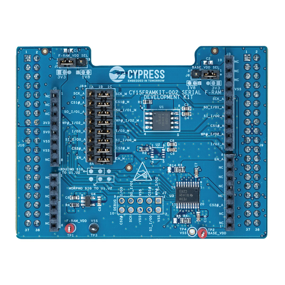
Page 25: Cy15Framkit-002 Kit Component Placements
Arduino Header (J3) Arduino Header (J1) F-RAM, SOIC package (U1) F-RAM, GQFN package (U2) Arduino Header (J4) Arduino Header (J2) Voltage Regulator (U4) Level Shifter (U3) Debug header (J7) CY15FRAMKIT-002 Serial F-RAM Development Kit User Guide, Document Number: 002-23147 Rev. *A... -
Page 26: Cy15Framkit-002 Kit Schematic
Appendix CY15FRAMKIT-002 Kit Schematic CY15FRAMKIT-002 Serial F-RAM Development Kit User Guide, Document Number: 002-23147 Rev. *A... -
Page 27: Pin Assignment Table
SCL / D15 J4 Connector (8 pins) ST Controller Arduino Signal CY15FRAMKIT-002 Kit Signals Signals J4_1 RX/D0 PA3/PA10 J4_2 TX/D1 PA2/PA9 J4_3 PA12 CS2#_A J4_4 PWM / D3 J4_5 CY15FRAMKIT-002 Serial F-RAM Development Kit User Guide, Document Number: 002-23147 Rev. *A... - Page 28 J9_20 J9_21 J9_22 SI_I/O0_M J9_23 EN_M J9_24 WP#_I/O2_M J9_25 PB10 SCK_M J9_26 I/O3_M J9_27 PA15 J9_28 J9_29 J9_30 J9_31 J9_32 AGND J9_33 PA12 CS2#_M J9_34 J9_35 PA2/PA9 J9_36 CY15FRAMKIT-002 Serial F-RAM Development Kit User Guide, Document Number: 002-23147 Rev. *A...
- Page 29 J10_16 J10_17 PA14 J10_18 J10_19 J10_20 J10_21 J10_22 J10_23 PC13 J10_24 J10_25 PC14 J10_26 J10_27 PC15 J10_28 J10_29 J10_30 J10_31 J10_32 J10_33 VBAT J10_34 J10_35 J10_36 J10_37 J10_38 CY15FRAMKIT-002 Serial F-RAM Development Kit User Guide, Document Number: 002-23147 Rev. *A...
-
Page 30: Use Of Zero-Ohm And No-Load Resistors
Solder R12 which will connect signals from J8B (J8_1B – J8_8B) to F-RAM Device (U1, U2) directly SO_I/O1 Solder R13 which will connect signals from J8B (J8_1B – J8_8B) to F-RAM Device (U1, U2) directly SI_I/O0 CY15FRAMKIT-002 Serial F-RAM Development Kit User Guide, Document Number: 002-23147 Rev. *A... -
Page 31: Bill Of Materials (Bom)
CY15FRAMKIT-002 Kit Signals (Arduino Signal) J8_1A J8_1B SCK_A J8_2A J8_2B CS1#_A J8_3A J8_3B SO_I/O1_A J8_4A J8_4B WP#_I/O2_A J8_5A J8_5B I/O3_A J8_6A J8_6B SI_I/O0_A J8_7A J8_7B CS2#_A J8_8A J8_8B EN_A CY15FRAMKIT-002 Serial F-RAM Development Kit User Guide, Document Number: 002-23147 Rev. *A... - Page 32 CY15FRAMKIT-002 Kit Signals (Morpho Signal) J8_1B J8_1C SCK_M J8_2B J8_2C CS1#_M J8_3B J8_3C SO_I/O1_M J8_4B J8_4C WP#_I/O2_M J8_5B J8_5C I/O3_M J8_6B J8_6C SI_I/O0_M J8_7B J8_7C CS2#_M J8_8B J8_8C EN_M CY15FRAMKIT-002 Serial F-RAM Development Kit User Guide, Document Number: 002-23147 Rev. *A...
-
Page 33: Appendix
This section is applicable only if the user includes the guiMENU (.c/.h) files in the project. The API provided in these files allows for testing the QSPI F-RAM device mounted on the CY15FRAMKIT-002 board by sending commands over the serial interface to the controller. - Page 34 Prints out current Register Latency setting. “804” Updates the Register latency value with new value. Function will fail if user attempts to set the latency higher than 3. CY15FRAMKIT-002 Serial F-RAM Development Kit User Guide, Document Number: 002-23147 Rev. *A...
- Page 35 Appendix Figure 16. GUI Menu CY15FRAMKIT-002 Serial F-RAM Development Kit User Guide, Document Number: 002-23147 Rev. *A...
- Page 36 Figure 19: Write/Read Example In this write/read example, 8 bytes are written starting from address location 16. Next, a read operation is performed for 16 locations starting from address 12. CY15FRAMKIT-002 Serial F-RAM Development Kit User Guide, Document Number: 002-23147 Rev. *A...
-
Page 37: Revision History
Revision Issue Date Origin of Description of Change Change 12/14/2018 NILE/GVCH New Spec 05/23/2019 GVCH Section 2.1: Updated J8 description Section 2.2.7 and Figure 6: Updated J8 description CY15FRAMKIT-002 Serial F-RAM Development Kit User Guide, Document Number: 002-23147 Rev. *A...
Need help?
Do you have a question about the CY15FRAMKIT-002 and is the answer not in the manual?
Questions and answers