
Related Manuals for Advantech PCL-818L


Summary of Contents for Advantech PCL-818L
- Page 2 Co., Ltd. assumes no responsibility for its use, nor for any infringe- ments of the rights of third parties which may result from its use. PC-LabCard is a trademark of Advantech Co., Ltd. IBM and PC are trademarks of International Business Machines Corporation. MS- DOS, Microsoft C and QuickBASIC are trademarks of Microsoft Corporation.
-
Page 3: Table Of Contents
Introduction ................ 2 Features ................2 Specifications ..............3 Daughterboards ..............5 Software support ..............7 Initial inspection .............. 10 Switch and jumper settings ..........10 Connector pin assignments ..........16 Hardware installation ............19 Software installation ............20 Analog input connections ..........22 Expanding analog inputs .......... - Page 4 Counter read/write and control registers ......50 Counter operating modes ..........53 Counter operations ............55 Counter applications ............56 Using DMA transfer with the PCL-818L ......59 VR assignment ..............68 A/D calibration ..............69 D/A calibration ..............69...
- Page 5 Chapter 1 General information...
- Page 6 A/D conversion with DMA and individual channel gains. The PCL-818L is an advanced new version of our popular PCL-818. A custom 160-pin ASIC chip integrates the functions of the full-size PCL-818. This chip gives you maximum accuracy and reliability, along with minimum cost, size and power consumption.
- Page 7 • Channels: 16 single-ended or 8 differential, switch selectable • Resolution: 12 bits • Input ranges (bipolar, V ±0.625, ± 1.25, ±2.5, ±5 or ±1.25, ± 2.5, ±5, ±10 All input ranges are software programmable. • Overvoltage: Continuous ±30 V max. •...
- Page 8 Pacer channel 0: Internal 100 KHz or external clock (10 MHz max). Source selected with Timer/Counter Enable Register (BASE+10) • Pacer output: 0.00023 Hz (71 minutes/pulse) to 2.5 MHz • Level: IRQ 2 to 7, software selectable • Enable: Via INTE bit of Control Register (BASE+9) PCL-818L User's Manual...
- Page 9 • Operating temp: 0 to +50 • Storage temp: -20 to +65 We offer a wide variety of optional daughterboards to help you get the most from your PCL-818L. You will need the PCLD-774 Analog Expansion Board or PCLD-8115 Wiring Terminal Board to make connections.
- Page 10 This board holds eight opto-isolated solid state relay modules and provides an additional eight outputs to drive external relays. These boards let you control relays through the PCL-818L's 16-bit digital output channels. PCLD-785B provides 24 SPDT relays, while the PCLD-885 provides 16 SPST power relays.
-
Page 11: Features
The PCL-818L comes with a powerful and easy-to-use software driver whose functions can be accessed by referring to a user-defined Parameter Table. With these driver functions your application pro- gramming becomes much easier, especially when you want to use some of the sophisticated features available from the PCL-818L, such as interrupt or DMA data transfer. - Page 12 16 channels of acquired data to disk. It can store at up to 200 KB/sec with no limitations on file size. Advantech Contact your local PC-LabCard representative for more information about these software packages. PCL-818L User's Manual...
- Page 13 Chapter 2 Installation...
-
Page 14: Specifications
It should be free of marks and scratches and in perfect order on receipt. As you unpack the PCL-818L, check it for signs of shipping damage (damaged box, scratches, dents, etc.). If it is damaged or fails to meet specifications, notify our service department or your local sales representative immediately. - Page 15 We set the PCL-818L for a base address of Hex 300 at the factory. If you need to adjust it to some other address range, set switch SW1 as shown in the following table: Range (hex) Switch position 000 - 00F...
- Page 16 You have two choices: DI0 (pin 1) on connector CN2 or TRIG0 (pin 35) on CN3. TRIG0 DI0 (default) TRIG0 TRIG0 You have two choices: DI2 (pin 3) on connector CN2 or GATE0 (pin 36) on CN3. GATE0 DI2 (default) GATE0 GATE0 PCL-818L User's Manual...
- Page 17 This setting has the same effect as that achieved by SW6 positions 7 and 8 on the PCL-718 card. Jumper JP4 selects reference voltage source for the PCL-818L's D/A converters. You can use the card's internal reference or supply an external reference.
- Page 18 If you use an internal reference voltage (set with JP4), the PCL-818L provides a choice of DC internal reference voltage sources: -5 V and - 10 V. JP5 selects the source, as shown below: -10 V -5 V (default) The PCL-818L offers 16 single-ended or eight differential analog input channels.
-
Page 19: Daughterboards
Jumpers JP8 to JP11 switch digital output channels 0 to 3 between the card's 20-pin connector and 37-pin connector. If you set the jumpers to the left (D) side, the digital output signals will come out on connec- tor CN1 (20-pin). If you set the jumpers to the right (S) side, the output signals will come out on connector CN3 (37-pin). -
Page 20: Connector Pin Assignments
The PCL-818L has two on-board 20-pin flat-cable connectors (insulation displacement, mass termination) and a DB-37 connector accessible from the card bracket. See the figure in Appendix B for the location of each connector. Connector pin assignments appear below. A/D S... - Page 21 D/I 0 D/I 1 D/I 2 D/I 3 D/I 4 D/I 5 D/I 6 D/I 7 D/I 8 D/I 9 D/I 10 D/I 11 D/I 12 D/I 13 D/I 14 D/I 15 D.GND D.GND +5 V +12 V A/DS0 A/DS8 A/DS1 A/DS9 A/DS2...
- Page 22 +5 V Note: Jumpers JP8 to JP11 select the output connector (either CN1 or CN3) for digital output signals 0 to 3. If you switch the output to CN1, no signals will appear on CN3, and vice versa. PCL-818L User's Manual...
-
Page 23: Hardware Installation
Save the screw to secure the interface card retaining bracket. 6. Carefully grasp the upper edge of the PCL-818L card. Align the hole in the retaining bracket with the hole on top of the expansion slot and align the gold striped edge connector with the expansion slot socket. - Page 24 The PCL-818L includes a floppy disk with utility software. The disk contains the following: 1. A comprehensive I/O driver for A/D, D/A, digital I/O and counter applications. This driver lets you use standard functions, written in common programming languages, to operate the PCL-818L. You do not need to perform detailed register programming.
- Page 25 Chapter 3 Signal connections...
- Page 26 PC and other hardware. This chapter provides information on signal connections for different types of data acquisi- tion applications. The PCL-818L supports either 16 single-ended or eight differential analog inputs. Jumper JP7 selects the input channel configuration. The major difference between single-ended and differential input connections is the number of signal wires per input channel.
- Page 27 If the signal source has one side connected to a local ground, the HIGH A.GND signal source ground and the PCL-818L ground will not be at exactly the same voltage, as they are connected through the ground return of the equipment and building wiring. The difference between the ground voltages forms a common-mode voltage.
- Page 28 HIGH Vin=Vs+Vcm You can expand any or all of the PCL-818L's A/D input channels with multiplexing daughterboards. Most daughterboards require the PCLD-774 Analog Expansion Board or the PCLD-8115 Screw Terminal Board for connections. The PCLD-789 Amplifier and Multiplexer multiplexes 16 differential inputs to one A/D input channel.
- Page 29 The PCL-818L provides one D/A output channel. You can use the internal precision -5 V or -10 V reference to generate 0 to +5 V or 0 to +10 V D/A output. For other D/A output ranges, use an external reference.
- Page 30 To receive an OPEN/SHORT signal from a switch or relay, add a pull- up resistor to ensure that the input is held at a high level when the contacts are open. See the figure below: 4.7K D.GND PCL-818L User's Manual...
- Page 31 Chapter 4 Register structure and format...
- Page 32 The key to programming the PCL-818L is to understand the function of the card's 16 registers. The PCL-818L requires 16 consecutive addresses in the PC's I/O space. Each address corresponds to a card register. The address of each register is specified as an offset from the card's base address.
- Page 33 Two read-only registers at BASE+0 and BASE+1 hold A/D conver- sion data. The 12 bits of data from the conversion are stored in BASE+1 bit 7 to bit 0 and BASE+0 bit 7 to bit 4. BASE+0 bits 3 to 0 store the source A/D channel number.
- Page 34 The high nibble provides the stop scan channel number, and the low nibble provides the start scan channel number. The MUX is initialized automatically to the start channel when you write to this register. Each A/D trigger sets the MUX to the next channel. PCL-818L User's Manual...
- Page 35 With continuous triggering the MUX will scan from the start channel to the end channel, then repeat. For example, if the start channel is 3 and the stop channel is 7, then the scan sequence is 3, 4, 5, 6, 7, 3, 4, 5, 6, 7, 3, 4...
- Page 36 The PCL-818L offers 16 digital input channels and 16 digital output channels. These I/O channels use the input and output ports at address BASE+3 and BASE+11. Value Value Value DI15 DI14 DI13 DI12 DI11 DI10 Value DO15 DO14 DO13 DO12...
- Page 37 Read-only register BASE+8 provides information on the A/D configu- ration and operation. Writing to this I/O port with any data value clears the its INT bit. The other data bits do not change. Value End of Conversion. The A/D converter is idle, ready for the next conversion.
- Page 38 818L will generate an interrupt when it completes an A/D conversion. Use this setting for interrupt driven data transfer. If DMAE = 1 the PCL-818L will generate an interrupt when it receives a T/C (terminal count) signal from the PC's DMA controller, indicating that a DMA transfer has completed.
- Page 39 Enables DMA transfer. Each A/D conversion initiates two successive DMA request signals. These signals cause the 8237 DMA controller to transfer two bytes of conversion data from the PCL-818L to memory. Note: You must program the PC's 8237 DMA controller and the DMA page register before you set DMAE to 1.
- Page 40 Write register BASE+10 enables or disables the PCL-818L's timer/ counter Value Disable/enable pacer Pacer enabled Pacer controlled by TRIG0. This blocks trigger pulses sent from the pacer to the A/D until TRIG0 is taken high. Counter 0 input source mode...
- Page 41 Chapter 5 A/D conversion...
- Page 42 This chapter explains how to use the PCL-818L's A/D conversion functions. The first five sections cover A/D data format, input range selection, status register settings, MUX scan setting, trigger modes and data transfer. The last section gives step by step implementation guidelines for A/D operations.
- Page 43 BASE+2. Bits D0 to D3 hold the starting channel number, and positions D4 to D7 hold the stop scan channel number. When you set the PCL-818L for eight differential input channels, bits CH3 and CL3 must be zero.
- Page 44 A/D applications because the triggering rate is too slow. 2. You can use the PCL-818L's on-board Intel 8254 programmable interval timer/counter to generate timing related signals. Counters 1 and 2 of the Intel 8254 can provide A/D converter trigger pulses with precise periods.
- Page 45 3. Direct memory access (DMA) transfer moves the A/D data from the PCL-818L hardware device to the PC system memory without the system CPU. DMA is very useful in high speed data transfer, but it is complicated to operate. Before the DMA operation you must set the DMA level (JP3), the DMA enable bit control register (BASE+9) and the registers in the 8237 DMA controller.
- Page 46 Your program can perform A/D by writing all the I/O port instructions directly, or you can take advantage of the PCL-818L driver. We suggest that you make use of the driver functions in your program. This will make your programming job easier and improve your program's performance.
- Page 47 Chapter 6 D/A conversion...
- Page 48 D/A converter. This double buffering process protects D/A data integrity through a single step update. The PCL-818L provides a precision fixed internal -5 V or -10 V reference, selectable by means of Jumper JP5. This reference voltage is available at connector CN3 pin 11.
- Page 49 The PCL-818L supports a variety of D/A operations. It can function as a digital attenuator (by inputting variable AC or DC references) or as a generator of arbitrary waveforms. In your application program you can perform D/A functions by addressing the PCL-818L's registers directly, or you can take advan- tage of the Advantech driver functions.
- Page 50 PCL-818L User's Manual...
- Page 51 Chapter 7 Digital input and output...
-
Page 52: Digital Signal Connections
The PCL-818L provides 16 digital input channels and 16 digital output channels. You read digital input data from registers BASE+3 and BASE+11. After the read operation the input lines go to three- state (data is not latched). You write digital output data to registers BASE+3 and BASE+11. The registers latch the output value (you can read it back). - Page 53 Chapter 8 Programmable counter/timer...
- Page 54 A/D converter, but you can also access it for your own use from connector CN3 pin 37. Counter 0 is not used by the PCL-818L and is available for your use. You can access it through CN3 pin 18.
- Page 55 The data format for the control register appears below: Value SC1 & SC0 Select counter. Counter Read-back command RW1 & RW0 Select read/write operation Operation Counter latch Read/write LSB Read/write MSB Read/write LSB first, then MSB M2, M1 & M0 Select operating mode Mode 0 interrupt on terminal count...
- Page 56 If you set both SC1 and SC0 to 1 and STA to 0, the register selected by C2 to C0 contains a byte which shows the status of the counter. The data format of the counter read/write register then becomes: Value PCL-818L User's Manual...
- Page 57 Current state of counter output Null count is 1 when the last count written to the counter register has been loaded into the counting element The counter enable register, located at address BASE+10, has a close relationship with the counter operation. Refer to Chapter 4, Timer/ counter enable register, for the register data format.
- Page 58 After the mode is set, the output will be high. When the count is loaded, the counter will begin counting. On terminal count, the output will go low for one input clock period then go high again. PCL-818L User's Manual...
- Page 59 If you reload the count register during counting, the new count will be loaded on the next CLK pulse. The count will be inhibited while the GATE input is low. The counter will start counting after the rising edge of the trigger input and will go low for one clock period when the terminal count is reached.
- Page 60 A subsequent read operation on the selected counter will retrieve the latched value. The 8254 programmable interval timer/counter on your PCL-818L interface card is a very useful device. You can program counters 1 and 2 to serve as a pacer to generate A/D conversion trigger pulses.
- Page 61 Chapter 9 Direct memory access operation...
- Page 62 Direct memory access (DMA) improves system performance by allowing external devices to transfer information directly to or from the PC's memory without using the CPU. The PCL-818L's DMA capability significantly improves the system performance in high speed A/D applications. The 8237 DMA controller chip on the PC system board handles the DMA operation.
- Page 63 1. When you configure your hardware, check your to see which (if any) PC DMA channel is available (level 1 or level 3) and set PCL-818L jumper JP1 accordingly. 2. If you will be using the PCL-818L driver for your DMA transfer programming, see the Software Drivers User’s Manual for information.
- Page 64 PCL-818L User's Manual...
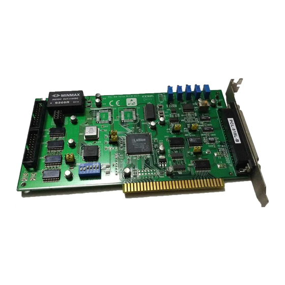
- Page 66 Appendix B Connector, Switch and VR Locations...
- Page 67 Differential or single-ended inputs A/D input voltage range selection (±5 or ±10) JP8 to JP11 Digital output connector, CN1 or CN3 (daughterboard ctrl.) A/D full scale A/D bipolar offset D/A full scale D/A offset PGA offset Test point 1 PCL-818L User's Manual...
- Page 68 Appendix C PC I/O port address map 65...
- Page 69 378 - 37F LPT1: (1st printer port) 380 - 3AF Reserved 3B0 - 3BF Mono Display/Print adapter 3C0 - 3CF Reserved 3D0 - 3DF Color/Graphics 3E0 - 3EF Reserved 3F0 - 3F7 Floppy disk drive 3F8 - 3FF COM1: PCL-818L User's Manual...
- Page 70 Appendix D Calibration...
- Page 71 Regular calibration checks are important to maintain accuracy in data acquisition and control applications. We provide a calibration pro- gram, CALB.EXE, on the PCL-818L software disk to assist you in this task. The minimum equipment required to perform a satisfactory calibration is a 4½-digit digital multimeter and a voltage calibrator or a stable,...
- Page 72 If you precisely calibrate a D/A output range, you can use the it with the CALB.EXE program to calibrate the card's A/D input. To calibrate the ±10 V A/D range, first calibrate the 0 to 10 V D/A output. To calibrate the ±5 V A/D range, first calibrate the 0 to 5 V D/A output.
- Page 73 PCL-818L User's Manual...
- Page 74 The purpose of this 'User's Note' is to inform you of the new jumper settings on the PCL-818L revised A2 card. If your PCL-818L card is revision A1, this note will not apply to you. The revision change is to simplify the multiplexing capability of the PCL-818L.
- Page 75 PCL-818L User's Manual...
Need help?
Do you have a question about the PCL-818L and is the answer not in the manual?
Questions and answers