Table of Contents
Advertisement
Quick Links
Advertisement
Table of Contents

Related Manuals for Advantech PCL-818 Series


Summary of Contents for Advantech PCL-818 Series
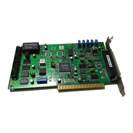
- Page 1 PCL-818 Series 12-bit ISA Multifunction Card User Manual...
- Page 2 No part of this man- ual may be reproduced, copied, translated or transmitted in any form or by any means without the prior written permission of Advantech Co., Ltd. Information provided in this manual is intended to be accurate and reli- able.
- Page 3 Product Warranty (2 years) Advantech warrants to you, the original purchaser, that each of its prod- ucts will be free from defects in materials and workmanship for two years from the date of purchase. This warranty does not apply to any products which have been repaired or...
-
Page 4: Declaration Of Conformity
This product has passed the CE test for environmental specifications when shielded cables are used for external wiring. We recommend the use of shielded cables. This kind of cable is available from Advantech. Please contact your local supplier for ordering information. - Page 5 Safety Instructions Read these safety instructions carefully. Keep this User's Manual for later reference. Disconnect this equipment from any AC outlet before cleaning. Use a damp cloth. Do not use liquid or spray detergents for clean- ing. For plug-in equipment, the power outlet socket must be located near the equipment and must be easily accessible.
- Page 6 The sound pressure level at the operator's position according to IEC 704- 1:1982 is no more than 70 dB (A). DISCLAIMER: This set of instructions is given according to IEC 704-1. Advantech disclaims all responsibility for the accuracy of any statements contained herein. PCL-818 Series User Manual...
-
Page 7: Table Of Contents
Chapter 2 Installation ............. 12 Unpacking ............... 12 Driver Installation ............13 Figure 2.1:Advantech Automation Software Setup ..13 Figure 2.2:Options for Driver Setup ......14 Hardware Installation ............. 15 Device Setup & Configuration........16 Figure 2.3:Device Manager ......... 16 Figure 2.4:Device Settings ........... - Page 8 FIFO Status — BASE+19H ..........61 C.19 FIFO Clear — BASE+19H ..........62 Appendix D Calibration ............. 64 VR Assignment .............. 65 Figure D.1:PCL-818HD/HG/L VR Assignment ..65 A/D Calibration ............... 66 D/A Calibration ............... 66 PCL-818 Series User Manual viii...
- Page 9 Overview Sections include: • Introduction • Features • Applications • Installation guide • Software Overview • Device Driver Roadmap • Accessories...
-
Page 10: Chapter 1 Overview
A/D conversion with DMA and individual gains for each channel. The PCL-818HD uses a CPLD chip designed in-house by Advantech engineers. This single chip integrates most of the card's functions, giving you maximum accuracy and reliability, along with minimum cost, size and power consumption. -
Page 11: Features
1.2 Features • 16 single-ended or eight differential analog inputs, switch selectable • 12-bit A/D, up to 100 KHz sampling rate with DMA transfer and differ- ent gain for each channel • Software-selectable gain: x 0.5, 1, 2, 4 or 8 •... -
Page 12: Applications
Note: For detailed specifications of the PCL-818HD/HG/L, please refer to Appendix A, Specifications. 1.3 Applications • Transducer and sensor measurements • Waveform acquisition and analysis • Process control and monitoring • Vibration and transient analysis PCL-818 Series User Manual... -
Page 13: Installation Guide
Before you install your PCL-818HD/HG/L card, please make sure you have the following necessary components: • PCL-818HD/HG/L DA&C Card • PCL-818HD/HG/L User’s Manual • Driver Software Advantech DLL drivers (included in the CD-ROM) • Wiring Cable PCL-10120/10137 (option) • Wiring Board... -
Page 14: Figure 1.1:Installation Flow Chart
Figure 1.1: Installation Flow Chart PCL-818 Series User Manual... -
Page 15: Software Overview
Device Drivers The Advantech Device Drivers software is included on the companion CD-ROM at no extra charge. It also comes with all the Advantech DA&C cards. Advantech’s Device Drivers features a complete I/O function library to help boost your application performance. The Advantech... -
Page 16: Device Driver Roadmap
• C++ Builder For instructions on how to begin programming works in each develop- ment tool, Advantech offers a Tutorial Chapter in the Device Drivers Manual for your reference. Please refer to the corresponding sections in this chapter on the Device Drivers Manual to begin your programming efforts. - Page 17 Programming with Device Drivers Function Library Advantech Device Drivers offer a rich function library that can be uti- lized in various application programs. This function library consists of numerous APIs that support many development tools, such as Visual C++, Visual Basic, Delphi and C++ Builder.
-
Page 18: Accessories
1.7 Accessories Advantech offers a complete set of accessory products to support the PCL-818HD/HG/L card. These accessories include: Wiring Cables • PCL-10120 The PCL-10120 cable is a 20-pin flat cable for PCL- 818HD/HG/L cards. • PCL-10137 The PCL-10137 shielded cable is specially designed for PCL-818HD/HG/L cards to provide high resistance to noise. - Page 19 Installation Sections include: • Unpacking • Driver Installation • Hardware Installation • Device Setup & Configuration...
-
Page 20: Chapter 2 Installation
Do not install a damaged card into your system. Note: Keep the anti-static bag for future use. You might need the original bag to store the card if you have to remove the card from PC or transport it elsewhere. PCL-818 Series User Manual... -
Page 21: Driver Installation
818HD/HG/L card into your system, since this will guarantee a smooth installation process. The Advantech Device Drivers Setup program for the PCL-818HD/HG/L card is included in the companion CD-ROM that is shipped with your DA&C card package. Please follow the steps below to install the driver software: Step 1: Insert the companion CD-ROM into your CD-ROM drive. -
Page 22: Figure 2.2:Options For Driver Setup
Figure 2.2: Options for Driver Setup For further information on driver-related issues, an online version of the Device Drivers Manual is available by accessing the following path: Start/Advantech Automation/Device Manager/Device Driver’s Manual PCL-818 Series User Manual... -
Page 23: Hardware Installation
Step 9: Plug in the power cord and turn on the computer. After your card is properly installed on your system, you can now config- ure your device using the Advantech Device Manager Program that has itself already been installed on your system during driver setup. A com- plete device installation procedure should include device setup, configu- ration and testing. -
Page 24: Device Setup & Configuration
2.4 Device Setup & Configuration The Advantech Device Manager program is a utility that allows you to set up, configure and test your device, and later stores your settings on the system registry. These settings will be used when you call the APIs of Advantech Device Drivers. -
Page 25: Figure 2.4:Device Settings
Step 3:Scroll down the List of Devices box to find the device that you wish to install, then click the Add… button. You will see a Device Setting dialog box such as the one in Fig. 2-4. Configuring the Device Step 4:On the Device Setting dialog box (Fig. -
Page 26: Figure 2.5:Device Name
Figure 2.5: Device Name After your card is properly installed and configured, you can click the Test… button to test your hardware by using the testing utility supplied. PCL-818 Series User Manual... -
Page 27: Figure 2.6:Test Utility
Figure 2.6: Test Utility For more detailed information, please refer to Chapter 2 of the Device Drivers Manual. You can also find the rich examples on the CD-ROM to speed up your programming. Chapter 2... - Page 28 PCL-818 Series User Manual...
-
Page 29: Signal Connections
Signal Connections Sections include: • Overview • Switch & Jumper Settings • Signal Connections • Field Wiring Considerations... -
Page 30: Chapter 3 Signal Connections
PCL- 818HD/HG/L via the I/O connector. 3.2 Switch & Jumper Settings The PCL-818HD/HG/L card has one function switch and five jumper set- tings. Figure 3.1: Connectors, Jumpers& Switches PCL-818 Series User Manual... - Page 31 Base Address Selection (SW1) You control the PCL-818HD/HG/L's operation by reading or writing data to the PC's I/O (input/output) port addresses. The PCL-818HD/HG/L requires 32 consecutive address locations with the FIFO buffer enabled or 16 locations with the FIFO disabled. Switch SW1 sets the card's base (beginning) address.
- Page 32 Jumpers Function Description Channel 3 (default) Channel 1 D/A Reference Voltage, Int./Ext. (JP11) Jumper JP11 selects reference voltage source for the PCL-818HD/HG/L's D/A converters. You can use the card's internal reference or supply an external reference. PCL-818 Series User Manual...
- Page 33 Table 3-3: Jumper JP11 Settings Jumpers Function Description JP11 External Internal (default) When you set JPI1 to INT, the D/A converter takes its reference voltage input from the card's on-board reference. Jumper JP10 selects either -5 V or -10 V on-board reference voltage. With JP11 set to INT the D/A chan- nel has an output range of 0 to +5 V or 0 to +10 V, respectively.
- Page 34 Fclk is 1 MHz or 10 MHz, as set by jumper JP8. Div l and Div2 are the dividers set in counter 1 and counter 2 in the 8254. See Chapter 8 for more details. Table 3-5: Jumper JP8 Settings Jumpers Function Description 1 MHz (default) 10 MHz PCL-818 Series User Manual...
- Page 35 FIFO Enable/Disable (JP6) When you enable the PCL-818HD/HG 's FIFO (First In First Out) buffer, each time the card makes an A/D reading, it will store the data in both the A/D output registers (accessed at addresses BASE+0/1) and in the FIFO buffer (accessed at BASE+23/24).
- Page 36 DB-37 connector, such as the PCLD-789D, read the digital output signals from the DB-37 connector (CN3). With other daughter boards you will need to connect an external 20-pin flat cable from CN1 to the daughter board. PCL-818 Series User Manual...
- Page 37 Table 3-8: Jumper Settings Jumpers Function Description JP1 (first) D0 (default) JP1 (second) D1 (default) JP1 (third) D2 (default) JP1 (fourth) D3 (default) Chapter 3...
-
Page 38: Signal Connections
Counter 0 CLK 17 36 Counter 0 GATE Counter 0 OUT 18 37 PACER Counter 0 OUT 18 37 PACER +5 V 19 +5 V 19 Note: The S0/S1 is NC, and S2/S3 is AGND for PCL-818HG PCL-818 Series User Manual... -
Page 39: I/O Connector Signal Description
3.3.2 I/O Connector Signal Description Table 3-9 I/O Connector Signal Descriptions Signal Name Reference Direction Description A/D S <0..15> A.GND Input Analog input (single-ended), channels 0 through A/D H <0..7> A.GND Input Analog input high (differential), channels 0 through 7. A/D L <0..7>... - Page 40 PCL-818HD/HG/L ground directly. In some cases you may also need a wire connection between the PCL-818HD/HG/L ground and the signal source ground for better grounding. The following two dia- grams show correct and incorrect connections for a differential input with local ground: PCL-818 Series User Manual...
- Page 41 Correct Connection HIGH Vin=Vs Incorrect Connection HIGH Vin=Vs+Vcm Expanding Analog Inputs You can expand any or all of the PCL-818HD/HG/L's A/D input channels using multiplexing daughterboards. Daughterboards without D-type con- nectors require the PCLD-774 Analog Expansion Board. The PCLD-789(D) Amplifier and Multiplexer multiplexes 16 differential inputs to one A/D input channel.
-
Page 42: Figure 3.2:Analog Output Connections
Connector CN3 provides D/A signals. Important D/A signal connections such as input reference, D/A outputs and analog ground appear below: CN3-31 D/A REF IN CN3-30 D/A OUT CN3-9,10,28,29 A.GND JP11 ON-Board CN3-11 VREF -10V JP10 Figure 3.2: Analog Output Connections PCL-818 Series User Manual... - Page 43 Digital Signal Connections The PCL-818HD/HG/L has 16 digital input and 16 digital output chan- nels. The digital I/O levels are TTL compatible. The following figure shows connections to exchange digital signals with other TTL devices: TTL Devices D.GND D.GND To receive an OPEN/SHORT signal from a switch or relay, add a pull-up resistor to ensure that the input is held at a high level when the contacts are open.
-
Page 44: Field Wiring Considerations
The signals transmitted on the cable will be directly affected by the qual- ity of the cable. In order to ensure better signal quality, we recommend that you use the PCL-10137 shielded cable. PCL-818 Series User Manual... - Page 45 Specifications...
-
Page 46: Appendix A Specifications
Offset error: Adjustable to zero Gain 0.5,1 5,10 50,100 1000 Gain error 0.01 0.02 0.04 0.08 0.08 (% FSR) Ch Type S.E./D S.E./D SNR: 68 dB ENOB: 11 bits External TTL Trigger 0.4 V max. Input High 2.4 V min. PCL-818 Series User Manual... -
Page 47: Analog Output
A.2 Analog Output Channels Resolution 12-bit Output Range Using Internal Reference 0 ~ +5V, 0 ~ +10 V (Internal & External Reference) Using External Reference -10V ~ +10 V Accuracy Relative ±0.5 LSB Differential ±0.5 LSB (monotonic) Non-linearity Gain Error Adjustable to zero Slew Rate 10V/s... -
Page 48: Counter/Timer
+5 V @ 650 mA Temperature Max. +5 V @ 700 mA 0 ~ 60 °C (32 ~158°F) (refer to IEC 68-2-1,2) Operation Storage -20~85°C (-4~185°F) Relative Humidity 5~95%RH non-condensing (refer to IEC 68-2-3) Certification CE certified PCL-818 Series User Manual... - Page 49 Block Diagram...
-
Page 50: Appendix B Block Diagram
1 2 -b it A /D C o n v e rte r P ro g . G a in w ith A m p life r S a m p le a n d H o ld PCL-818 Series User Manual... - Page 51 Register Structure & Format...
-
Page 52: Appendix C Register Structure & Format
Drivers for user programming under the Windows 95/98/NT/2000/ME/ XP operating system. We advise users to program the PCL-818HD/HG/L using the 32-bit Device Drivers provided by Advantech to avoid the com- plexity of low-level registry programming. The most important consideration in programming the PCL-818HD/HG/ L the register level is to understand the function of the card's registers. - Page 53 Table C-1 PCL-818HD/HG/L Register Format (Part 1) Base Addr. +HEX A/D low byte data and channels Software A/D trigger A/D high byte data and channels AD11 AD10 AD9 A/D range control MUX scan channel status MUX scan channel control Digital Input (low byte) Digital Output (low byte) D/A output data D/A output data...
- Page 54 Digital Input (high byte) DI15 DI14 DI13 DI12 DI11 DI10 Digital Output (high byte) DO15 DO14 DO13 DO12 DO11 DO10 DO9 DO8 Counter 0 Counter 0 Counter 1 Counter 1 Counter 2 Counter 2 Counter Control PCL-818 Series User Manual...
-
Page 55: A/D Data & Channels - Base+00H~01H
Table C-1 PCL-818HD/HG/L Register Format (Part 3) Base Addr. +HEX Clear FIFO Interrupt Request A/D data and channels from FIFO A/D data and channels from FIFO AD11 AD10 AD9 FIFO status FIFO clear C.3 A/D Data & Channels — BASE+00H~01H Table C-2 Register for A/D Data &... -
Page 56: Software A/D Trigger - Base+00H
Table C-4 Register for A/D Range Control Write A/D range control Bit # BASE + 01H G3 ~ G0 A/D range control the least significant bit (LSB) of the A/D range the most significant bit (MSB) PCL-818 Series User Manual... - Page 57 Range codes appear below: PCL-818HD Input Range (V) Unipolar/Bipolar Gain Code -5 to +5 -2.5 to +2.5 -1.25 to +1.25 -0.625 to +0.625 0 to 10V 0 to 5V 0 to 2.5V 0 to 1.25V -10V to +10V PCL-818HG Input Range (V) Unipolar/Bipolar Gain Code ±5V...
-
Page 58: Mux Scan Channel Control - Base+02H
For example, if the start channel is 3 and the stop channel is 7, then the scan sequence is 3, 4, 5, 6, 7, 3, 4, 5, 6, 7, 3, 4.… PCL-818 Series User Manual... - Page 59 Table C-5 Register for MUX Scan Channel Control Write MUX scan channel control Bit # BASE + 02H CH3 ~ CH0 Stop scan channel number the least significant bit (LSB) of the stop channel the most significant bit (MSB) CL3 ~ CL0 Start scan channel number the least significant bit (LSB) of the start channel the most significant bit (MSB) The MUX scan register low nibble, CL3 to CL0, also acts as a pointer...
-
Page 60: Mux Scan Channel Status - Base+02H
Bit # BASE + 03H DO7 BASE + 0BH DO15 DO14 DO13 DO12 DO11 DO10 DO15 ~ DO0 Digital output data the least significant bit (LSB) of the DO data DO15 the most significant bit (MSB) PCL-818 Series User Manual... -
Page 61: D/A Output - Base+04/05H
Table C-8 Register for Digital Output Read Digital Input Bit # BASE + 03H BASE + 0BH DI15 DI14 DI13 DI12 DI11 DI10 DI15 ~ DI0 Digital input data the least significant bit (LSB) of the DI data DI15 the most significant bit (MSB) Note: Digital Outputs D0 - D3 is selectable from the 20- pin connector or the 37-pin D connector. -
Page 62: Fifo Interrupt Control - Base+06H
C.10 FIFO Interrupt Control — BASE+06H Table C-10 Register for FIFO Interrupt Control Write FIFO interrupt control Bit # BASE + 06H FINT FINT Enable/disable FIFO interrupt FIFO interrupt disabled FIFO interrupt enabled Note: This register is not used for PCL-818L. PCL-818 Series User Manual... -
Page 63: Clear Interrupt Request - Base+08H
C.11 Clear Interrupt Request — BASE+08H Write any value to register BASE+08H to clear the interrupt request. Table C-11 Register for Clear Interrupt Request Write A/D control Bit # BASE + 09H C.12 A/D Status — BASE+08H Read-only register BASE+08H provides information on the A/D configu- ration and operation. - Page 64 Your software should therefore wait for the signal INT = 1 before it reads the conversion data. It should then clear the INT bit by writing any value to the A/D status register BASE+08H. PCL-818 Series User Manual...
-
Page 65: A/D Control - Base+09H
C.13 A/D Control — BASE+09H Read/write register BASE+09H provides information on the PCL- 818HD/HG/L's operating modes. Table C-13 Register for A/D Control Read/Write A/D control Bit # BASE + 09H INTE DMAE INTE Disable/enable generated interrupts Disables the generation of interrupts. No interrupt signal can be sent to the PC bus. - Page 66 PCL-818HD/HG/L to memory. Note: You must program the PC's 8237 DMA controller the DMA page register before you set DMAE to 1. ST1 to ST0 Trigger source Trigger Source Software trigger External trigger Pacer trigger PCL-818 Series User Manual...
-
Page 67: Timer/Counter Enable - Base+0Ah
C.14 Timer/Counter Enable — BASE+0AH Write register BASE+0AH enables or disables the PCL-818HD/HG/L's timer/counter. Table C-14 Register for Timer/Counter Enable Write Timer/Counter enable Bit # BASE + 0AH TC0 Disable/enable pacer Pacer enabled Pacer controlled by TRIG0. This blocks trigger pulses sent from the pacer to the A/D until TRIG0 is taken high. -
Page 68: Clear Fifo Interrupt Request - Base+14H
(MSB) C3 ~ C0 A/D channel number from which the data is derived the least significant bit (LSB) of the channels the most significant bit (MSB) Note: This register is not used for PCL-818L. PCL-818 Series User Manual... -
Page 69: Fifo Status - Base+19H
C.18 FIFO Status — BASE+19H The register at BASE+19H clears the FIFO buffer and sets its empty flag (EF). The FIFO status register, address BASE+19H, has flags which you can read to determine the current state of the FIFO buffer, including full flag, half-full flag, and empty flag. -
Page 70: Fifo Clear - Base+19H
Writing any value to BASE+19H clears all data in the FIFO and sets the empty flag (EF) to 1. Table C-18 Register for FIFO Clear Write FIFO clear Bit # BASE + 19H Note: This register is not used for PCL-818L. PCL-818 Series User Manual... - Page 71 Calibration...
-
Page 72: Appendix D Calibration
DA&C card is already stable. A calibration program, CALB.EXE, is included on the CD-ROM: CALB.EXE PCL-818HD/HG/L calibration utility This calibration utility is designed for the Microsoft DOS environment. Access this program from the default location: C:\Program Files\Advantech\ADSAPI\Utilities\PCL818 PCL-818 Series User Manual... -
Page 73: Vr Assignment
D.1 VR Assignment The six variable resistors (VRs) on the PCL-818HD/HG/L board help you make accurate adjustment on all A/D and D/A channels. See the fig- ure in Appendix B for help finding the VRs. The following list shows the function of each VR: Function A/D unipolar offset... -
Page 74: A/D Calibration
Set the D/A data to 4095 and adjust VR5 until the D/A output voltage equals the reference voltage minus 1 LSB, but with the opposite sign, For example, if V is -5 V, then V should be +4.9988 V. PCL-818 Series User Manual...
Need help?
Do you have a question about the PCL-818 Series and is the answer not in the manual?
Questions and answers