Advertisement
Quick Links
Advertisement

Related Manuals for Advantech PCL-740


Summary of Contents for Advantech PCL-740
- Page 2 Advantech Co., Ltd. Information provid- ed in this manual is intended to be accurate and reliable. However, Advantech Co., Ltd. assumes no responsibility for its use, nor for any infringements of rights of third parties which may result from its use.
- Page 3 Description ................2 Features ..................3 Applications ...................3 Specifications .................4 Initial Inspection ..............8 PCL-740 Jumper and Switch Locations ......9 Card Configuration ............10 Jumper settings ..............12 Card installation ..............16 Register Structure ............... 18 Programming example ............21...
- Page 4 Chapter 1 Introduction...
- Page 5 I/O more reliable. By buffering data into 16-byte packets before putting it on the bus the UART drastically reduces the CPU load. This makes the PCL-740 especially suitable for high speed serial I/O applications and applications under MS Windows.
-
Page 6: Chapter 1 Introduction
• Serial Port can be configured to RS-232/422/485 or current-loop • 16C550 FIFO UART (with 16-byte FIFO) • Baud rate up to 115 Kbps • IRQ selection: 3, 4, 5, 6, 7, 9, 10, 11, 12 or 15 • Complete RS-232 modem-control signals •... - Page 7 • Signals: TxD, RxD, RTS, CTS, DTR, DSR, DCD, RI, GND • Mode: Asynchronous, full duplex • Baud-rate: 50 to 115200 bps • Stop bits: 1, 1.5, 2 • Parity: Even, odd or none • Data bits: 5, 6, 7, 8 PCL-740 User's Manual...
- Page 8 • Signal driver/Receiver: 6N136 • Signals: TxD+, TxD-, RxD+, RxD- • Current value: 20 mA (Standard) • Mode: Asynchronous, full duplex • Baud-rate: 50 to 115200 bps • Transmission distance: 1000 m • Signal driver/receiver: SN75176, SN75173 • Signals: TxD+, TxD-, RxD+, RxD-, RTS+, RTS-, CTS+, CTS-, GND •...
- Page 9 PCL-740 User's Manual...
- Page 10 Chapter 2 Hardware Installation...
- Page 11 It should be free of marks and scratches and in perfect working order on receipt. As you unpack the PCL-740, check it for signs of shipping damage (damaged box, scratches, dents, etc.). If it is damaged or it fails to meet specifications, notify our service department or your local sales representative immediately.
-
Page 12: Chapter 2 Hardware Installation
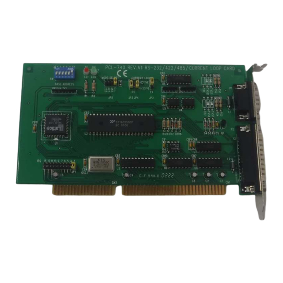
RS-232/Current-loop RS-422/485 Current-loop select Tx Active/Passive Rx Active/Passive Protocol Selection Base Address Selection Chapter 2 Hardware Installation... - Page 13 Each port of the PCL-740 card has two associated status jumper groups and one six position DIP switch. If you do not use the boards default settings then these all require configuring prior to use. I/O port base address, interrupt level, RS-232/422/485/current-loop driver mode and receiver status all require setting up.
- Page 14 The board will be shipped in the RS-232 mode. If your requirements are the same as this default setting, you may simply install the card without the need for any setting up. The PCL-740 DIP switch and jumper default settings are as shown below:...
- Page 15 Note: When either RS-232, RS-422 or RS-485 mode is selected, the two current-loop Tx/Rx active/passive jumpers are inoperable. Should you want to configure the PCL-740 to operate in the current- loop mode, configure the main jumper for current-loop. You also have to set Tx and Rx for active or passive mode.
- Page 16 The I/O base address the PC-740 is selectable by a 6 position DIP switch, SW1. Refer to page 9 for the locations of the DIP switch SW1. The base address can be set anywhere in the I/O address area from hex 200 to hex 3F8. If you have more than one card installed you must select a different base address for each card.
- Page 17 The switch sum is set to 2F8 = 200 + 80 + 40 + 20 + 10 + 8, (HEX). Base address Deci- line value value NOTE: On the PCL-740 the address line A9 is does not appear on the DIP switch as it is permanently hard-wired to HEX 200 on the card.
- Page 18 The PCL-740 card is designed to access interrupt levels 3 up to level 15 with the exception of 8, 13, and 14. If the card is to be designated as COM1:, the interrupt level must be set to IRQ4 (the default). For COM2: the setting is IRQ3.
- Page 19 (save the screw to secure the interface card retaining bracket). Remove the anti-vibration card clamp if supplied. 6. Carefully grasp the upper edge of the PCL-740 card. Align the hole in the retaining bracket with the hole on top of the expansion slot.
- Page 20 Appendix A Register structure and format...
- Page 21 The two bytes BASE+0 and BASE+1 together form a 16-bit number, the divisor, which determines the baud rate. Set the divisor as follows: Baud rate Divisor Baud rate Divisor 2304 2400 1536 3600 1047 4800 133.5 7200 9600 19200 38400 1200 56000 1800 115200 2000 PCL-740 User's Manual...
-
Page 22: Appendix A Register Structure And Format
BASE+1 Interrupt Status Register (ISR) when DLAB=0 bit 0 Enable received-data-available interrupt bit 1 Enable transmitter-holding-register-empty interrupt bit 2 Enable receiver-line-status interrupt bit 3 Enable modem-status interrupt BASE+2 FIFO Control Register (FCR) bit 0 Enable transmit and receive FIFOs bit 1 Clear contents of receive FIFO bit 2 Clear contents of transmit FIFO bits 6-7 Set trigger level for receiver FIFO interrupt. - Page 23 0 Delta CTS bit 1 Delta DSR bit 2 Trailing edge ring indicator bit 3 Delta received line signal detect bit 4 CTS bit 5 DSR bit 6 RI bit 7 Received line signal detect BASE+7 Temporary data register PCL-740 User's Manual...
- Page 24 The following C example shows how to program the PCL-740's registers directly. It uses I/O ports hex 3F8 and 2F8 to test the PCL- 740’s send, receive and FIFO functions. /**************************************************/ /* Program: DEMO01.C /* Description: Sends a string from COM1 to COM2 then reads it back from COM2 and displays it on the screen.
- Page 25 (max 15 char) or Q to quit:"); gets(cmd); while (cmd[0] != ‘q’ && cmd[0] != ‘Q’) /* Send string on Port 1 (COM1) */ i=0; cmd[strlen(cmd)] = 0x0d; flag=1; while (flag) outportb(base0,cmd[i]); /* Send data */ if (cmd[i] == 0x0d) flag=0; i++; PCL-740 User's Manual...
- Page 26 /* Receive data on Port 2 (COM2) */ i=0; flag=1; timeout=TIME_OUT; while (flag) /* Check for received data on port*/ if ((inportb(base1+5) & 1) !=0) rec[i]=inportb(base1); /* Receive data */ if (rec[i] == 0x0d) rec[i+1]=’\0'; flag=0; printf(“\nReceived data: %s\n”, rec); i++;...
- Page 27 PCL-740 User's Manual...
- Page 28 Appendix B: PC I/O Address Assignments...
- Page 29 The following table indicates the PC I/O address usage assignment. To prevent conflicting settings of the PCL-740 with other devices or I/O cards, you are recommended to refer this table. 000 - 00F DMA (8237A) 020 - 021 8259A IRQ Controller...
Need help?
Do you have a question about the PCL-740 and is the answer not in the manual?
Questions and answers