Table of Contents
Advertisement
Quick Links
MC9S08JS16
MC9S08JS8
MC9S08JS16L
MC9S08JS8L
Reference Manual
HCS08
Microcontrollers
MC9S08JS16RM
Rev. 4
4/2009
freescale.com
Related Documentation:
• MC9S08JS16 (Data Sheet)
Contains pin assignments and diagrams, all electrical
specifications, and mechanical drawing outlines.
Find the most current versions of all documents at:
http://www.freescale.com
Advertisement
Table of Contents

Related Manuals for Freescale Semiconductor MC9S08JS16 Series


Summary of Contents for Freescale Semiconductor MC9S08JS16 Series
- Page 1 MC9S08JS16 MC9S08JS8 MC9S08JS16L MC9S08JS8L Reference Manual Related Documentation: HCS08 Microcontrollers • MC9S08JS16 (Data Sheet) Contains pin assignments and diagrams, all electrical specifications, and mechanical drawing outlines. Find the most current versions of all documents at: http://www.freescale.com MC9S08JS16RM Rev. 4 4/2009 freescale.com...
- Page 3 MC9S08JS16 Features 8-Bit HCS08 Central Processor Unit (CPU) transceiver; supports endpoint 0 and up to 6 additional endpoints • 48 MHz HCS08 CPU (central processor • SPI — One 8- or 16-bit selectable serial unit) peripheral interface module with a receive •...
- Page 5 MC9S08JS16 MCU Series Reference Manual Covers: MC9S08JS16 MC9S08JS8 MC9S08JS16L MC9S08JS8L MC9S08JS16RM Rev. 4 4/2009...
- Page 6 Added MC9S08JS16L and MC9S08JS8L information. ® This product incorporates SuperFlash technology licensed from SST. Freescale and the Freescale logo are trademarks of Freescale Semiconductor, Inc. © Freescale Semiconductor, Inc., 2008-2009. All rights reserved. MC9S08JS16 MCU Series Reference Manual, Rev. 4 Freescale Semiconductor...
-
Page 7: Table Of Contents
Chapter 17 Development Support ....... . . 283 MC9S08JS16 MCU Series Reference Manual, Rev. 4 Freescale Semiconductor... - Page 9 3.6.2 Stop2 Mode ........................32 3.6.3 On-Chip Peripheral Modules in Stop Modes ..............33 Chapter 4 Memory MC9S08JS16 Series Memory Map ....................35 4.1.1 Reset and Interrupt Vector Assignments ................36 Register Addresses and Bit Assignments ..................37 RAM (System RAM) ........................43 USB RAM ............................44 Bootloader ROM ..........................44...
- Page 10 5.7.4 System Options Register 1 (SOPT1) ................73 5.7.5 System Options Register 2 (SOPT2) ................74 5.7.6 Flash Protection Defeat Register (FPROTD) ..............75 5.7.7 SIGNATURE Register (SIGNATURE) ................75 5.7.8 System Device Identification Register (SDIDH, SDIDL) ..........76 MC9S08JS16 MCU Series Reference Manual, Rev. 4 Freescale Semiconductor...
- Page 11 7.3.6 Indexed Addressing Mode ....................92 Special Operations ...........................93 7.4.1 Reset Sequence .........................93 7.4.2 Interrupt Sequence ......................93 7.4.3 Wait Mode Operation ......................94 7.4.4 Stop Mode Operation ......................94 7.4.5 BGND Instruction ......................95 HCS08 Instruction Set Summary ....................96 MC9S08JS16 MCU Series Reference Manual, Rev. 4 Freescale Semiconductor...
- Page 12 Initialization / Application Information ..................132 9.5.1 MCG Module Initialization Sequence ................132 9.5.2 MCG Mode Switching ....................133 9.5.3 Calibrating the Internal Reference Clock (IRC) .............144 Chapter 10 Modulo Timer (S08MTIMV1) 10.1 Introduction ...........................147 MC9S08JS16 MCU Series Reference Manual, Rev. 4 Freescale Semiconductor...
- Page 13 12.2.5 SCI Status Register 2 (SCIS2) ..................177 12.2.6 SCI Control Register 3 (SCIC3) ..................178 12.2.7 SCI Data Register (SCID) ....................179 12.3 Functional Description ........................179 12.3.1 Baud Rate Generation .....................179 12.3.2 Transmitter Functional Description ................180 MC9S08JS16 MCU Series Reference Manual, Rev. 4 Freescale Semiconductor...
- Page 14 Chapter 14 Timer/Pulse-Width Modulator (S08TPMV3) 14.1 Introduction ...........................215 14.2 Features ............................215 14.3 TPMV3 Differences from Previous Versions ................217 14.3.1 Migrating from TPMV1 ....................219 14.3.2 Features ...........................220 14.3.3 Modes of Operation ......................220 MC9S08JS16 MCU Series Reference Manual, Rev. 4 Freescale Semiconductor...
- Page 15 15.3.7 Error Interrupt Status Register (ERRSTAT) ..............253 15.3.8 Error Interrupt Enable Register (ERRENB) ..............254 15.3.9 Status Register (STAT) ....................255 15.3.10Control Register (CTL) ....................256 15.3.11Address Register (ADDR) ....................257 15.3.12Frame Number Register (FRMNUML, FRMNUMH) ...........257 MC9S08JS16 MCU Series Reference Manual, Rev. 4 Freescale Semiconductor...
- Page 16 17.3.6 Hardware Breakpoints ....................297 17.4 Register Definition ........................297 17.4.1 BDC Registers and Control Bits ..................297 17.4.2 System Background Debug Force Reset Register (SBDFR) ..........299 17.4.3 DBG Registers and Control Bits ..................300 MC9S08JS16 MCU Series Reference Manual, Rev. 4 Freescale Semiconductor...
-
Page 17: Chapter 1 Device Overview
Device Overview Introduction MC9S08JS16 series MCUs are members of the low-cost, high-performance HCS08 family of 8-bit microcontroller units (MCUs). All MCUs in the family use the enhanced HCS08 core and are available with a variety of modules, memory sizes, memory types, and package types. -
Page 18: Mcu Block Diagram
Chapter 1 Device Overview MCU Block Diagram The block diagram in Figure 1-1 shows the structure of the MC9S08JS16 series MCU. ON-CHIP ICE AND HCS08 CORE USBDP DEBUG MODULE (DBG) USBDN FULL SPEED BKGD/MS MODULE USB ENDPOINT TRANSCEIVER PTA0/KBIP0/TPMCH0 PTA1/KBIP1/MISO... -
Page 19: System Clock Distribution
The fixed frequency clock (FFCLK) is internally synchronized to the bus clock and must not exceed one half of the bus clock frequency. Flash and EEPROM have frequency requirements for program and erase operation. See MC9S08JS16 Series Data Sheet for details. - Page 20 TCLK — TCLK is the optional external clock source for the TPM or MTIM modules. The TCLK must be limited to 1/4th the frequency of the BUSCLK for synchronization. See Chapter 14, “Timer/Pulse-Width Modulator (S08TPMV3),” for more details. MC9S08JS16 MCU Series Reference Manual, Rev. 4 Freescale Semiconductor...
-
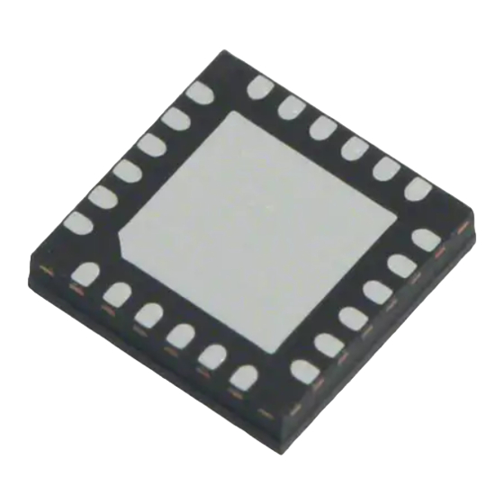
Page 21: Chapter 2 Pins And Connections
This chapter describes signals that connect to package pins. It includes a pinout diagram, a table of signal properties, and detailed discussion of signals. Device Pin Assignment PTB0/IRQ/TCLK PTA5/KBIP5/TPMCH1 PTB1/RESET USB33 PTB2/BKGD/MS 24-Pin QFN USBDP PTB3/BLMS USBDN PTA0/KBIP0/TPMCH0 Figure 2-1. MC9S08JS16 Series in 24-pin QFN Package MC9S08JS16 MCU Series Reference Manual, Rev. 4 Freescale Semiconductor... -
Page 22: Recommended System Connections
PTA0/KBIP0/TPMCH0 PTA1/KBIP1/MISO PTA4/KBIP4/SS PTA2/KBIP2/MOSI PTA3/KBIP3/SPSCK Figure 2-2. MC9S08JS16 Series in 20-Pin SOIC Package Recommended System Connections Figure 2-3 shows pin connections that are common to almost all MC9S08JS16 series application systems. MC9S08JS16 MCU Series Reference Manual, Rev. 4 Freescale Semiconductor... - Page 23 0.5 mA for a 10 kΩ resistor). The load on PTB2/PTB3 must be smaller than 50 pF. 10. When using internal V as supply, there needs to be an external cap. USB33 Figure 2-3. Basic System Connections MC9S08JS16 MCU Series Reference Manual, Rev. 4 Freescale Semiconductor...
-
Page 24: Power
After configured as RESET, the pin remains RESET until the next LVD or POR. The RESET pin when enabled can be used to reset the MCU from an external source when the pin is driven low. MC9S08JS16 MCU Series Reference Manual, Rev. 4 Freescale Semiconductor... -
Page 25: Background/Mode Select (Bkgd/Ms)
Small capacitances from cables and the absolute value of the internal pullup device play almost no role in determining rise and fall times on the BKGD pin. MC9S08JS16 MCU Series Reference Manual, Rev. 4 Freescale Semiconductor... -
Page 26: Bootloader Mode Select (Blms)
2.3.7 General-Purpose I/O and Peripheral Ports The MC9S08JS16 series of MCUs supports up to 14 general-purpose I/O pins, including two output-only pins, which are shared with on-chip peripheral functions (timers, serial I/O, keyboard interrupts, etc.). When a port pin is configured as a general-purpose output or a peripheral uses the port pin as an output, software can select one of two drive strengths and enable or disable slew rate control. - Page 27 Selecting a higher priority pin function with a lower priority function already enabled can cause spurious edges to the lower priority module. All modules that share a pin must be disabled before another module is enabled. MC9S08JS16 MCU Series Reference Manual, Rev. 4 Freescale Semiconductor...
- Page 28 Chapter 2 Pins and Connections MC9S08JS16 MCU Series Reference Manual, Rev. 4 Freescale Semiconductor...
-
Page 29: Chapter 3 Modes Of Operation
Chapter 3 Modes of Operation Introduction The operating modes of the MC9S08JS16 series are described in this section. Entry into each mode, exit from each mode, and functionality while in each mode are described. Features • Active background mode for code development •... -
Page 30: Wait Mode
The active background mode is used to program a bootloader or user application program into the flash program memory before the MCU is operated in run mode for the first time. When the MC9S08JS16 series devices are shipped from the Freescale factory, the flash program memory is erased by default unless specifically noted, so there is no program that could be executed in run mode until the flash memory is initially programmed. -
Page 31: Stop Modes
Some HCS08 devices that are designed for low-voltage operation (1.8 to 3.6 V) also include stop1 mode. The MC9S08JS16 series of MCUs do not include stop1 mode. Table 3-1 shows all of the control bits that affect stop mode selection and the mode selected under various conditions. -
Page 32: Stop2 Mode
To maintain I/O states for pins that are configured as general-purpose I/O before entering stop2, the user must restore the contents of the I/O port registers, which have been saved in RAM, to the port registers MC9S08JS16 MCU Series Reference Manual, Rev. 4 Freescale Semiconductor... -
Page 33: On-Chip Peripheral Modules In Stop Modes
EREFSTEN set in MCGC2, else in standby. For high frequency range (RANGE in MCGC2 set), the LVD must also be enabled in stop3. USBEN in CTL is set and USBPHYEN in USBCTL0 is set, else off. MC9S08JS16 MCU Series Reference Manual, Rev. 4 Freescale Semiconductor... - Page 34 Chapter 3 Modes of Operation MC9S08JS16 MCU Series Reference Manual, Rev. 4 Freescale Semiconductor...
-
Page 35: Chapter 4 Memory
MC9S08JS16 Series Memory Map Figure 4-1 shows the memory map for the MC9S08JS16 series. On-chip memory in the MC9S08JS16 series of MCUs consists of RAM, flash program memory for nonvolatile data storage, plus I/O and control/status registers. The registers are divided into three groups: •... -
Page 36: Reset And Interrupt Vector Assignments
The vector names shown in this table are the labels used in the Freescale-provided equate file for the MC9S08JS16 series. For more details about resets, interrupts, interrupt priority, and local interrupt mask controls, refer to Chapter 5, “Resets,... -
Page 37: Register Addresses And Bit Assignments
Therefore, care must be taken when using these locations if the code will be ported to other MCUs. Register Addresses and Bit Assignments The registers in the MC9S08JS16 series are divided into these three groups: MC9S08JS16 MCU Series Reference Manual, Rev. 4 Freescale Semiconductor... - Page 38 Cells that are not associated with named bits are shaded. A shaded cell with a 0 indicates this unused bit always reads as a 0. Shaded cells with dashes indicate unused or reserved bit locations that could read as 1s or 0s. MC9S08JS16 MCU Series Reference Manual, Rev. 4 Freescale Semiconductor...
- Page 39 Bit 7 Bit 0 0x0028– Reserved — — — — — — — — 0x002F 0x0030 SPIC1 SPIE SPTIE MSTR CPOL CPHA SSOE LSBFE 0x0031 SPIC2 SPMIE SPIMODE MODFEN BIDIROE SPISWAI SPC0 MC9S08JS16 MCU Series Reference Manual, Rev. 4 Freescale Semiconductor...
- Page 40 Reserved — — — — — — — — 0x006C 0x006D EPCTL0 EPCTLDIS EPRXEN EPTXEN EPSTALL EPHSHK 0x006E EPCTL1 EPCTLDIS EPRXEN EPTXEN EPSTALL EPHSHK 0x006F EPCTL2 EPCTLDIS EPRXEN EPTXEN EPSTALL EPHSHK MC9S08JS16 MCU Series Reference Manual, Rev. 4 Freescale Semiconductor...
- Page 41 Bit 15 Bit 8 0x1815 DBGFL Bit 7 Bit 0 0x1816 DBGC DBGEN BRKEN RWAEN RWBEN 0x1817 DBGT TRGSEL BEGIN TRG3 TRG2 TRG1 TRG0 0x1818 DBGS ARMF CNT3 CNT2 CNT1 CNT0 MC9S08JS16 MCU Series Reference Manual, Rev. 4 Freescale Semiconductor...
- Page 42 1. IFR — Nonvolatile information memory that can be only accessed during production test. During production test, system initialization, configuration and test information is stored in the IFR. This information cannot be read or modified in normal user or background debug modes. MC9S08JS16 MCU Series Reference Manual, Rev. 4 Freescale Semiconductor...
-
Page 43: Ram (System Ram)
For compatibility with older M68HC05 MCUs, the HCS08 resets the stack pointer to 0x00FF. In the MC9S08JS16 series, re-initialize the stack pointer to the top of the RAM so the direct-page RAM can be used for frequently accessed RAM variables and bit-addressable program variables. Include the following 2-instruction sequence in your reset initialization routine (where RamLast is equated to the highest address of the RAM in the Freescale-provided equate file). -
Page 44: Usb Ram
The BLMS pin of bootloader ROM decides whether the MCU will enter bootloader mode directly during power-on reset. This pin is only examined during Power-On Reset (POR). The signal properties of bootrom are shown in Table 4-5. MC9S08JS16 MCU Series Reference Manual, Rev. 4 Freescale Semiconductor... -
Page 45: Modes Of Operation
FLASHCRC 16-bit word. If the result matches, the user mode is entered. 3. When a reset occurs (other than a power-on reset), if the SIGNATURE semaphore is not equal to 0xC3, the user mode is entered. MC9S08JS16 MCU Series Reference Manual, Rev. 4 Freescale Semiconductor... -
Page 46: Flash Memory Map
Flash Block 0xFFB7 0xFFB8 Flash Block Checksum 0xFFB9 Checksum Bypass 0xFFBA 0xFFBB Flash Block 0xFFBD Flash Partial Erase semaphore 0xFFBE 0xFFBF Other Registers Vectors 0xFFFF 0xFFFF Figure 4-2. General Flash Memory Map MC9S08JS16 MCU Series Reference Manual, Rev. 4 Freescale Semiconductor... -
Page 47: Bootloader Operation
Flash block checksum calculation uses 16-bit CRC. JS16 flash block checksum range is 0xC400–0xFFAD and 0xFFC0–0xFFFF, JS8 flash block checksum range is 0xE400–0xFFAD and 0xFFC0–0xFFFF. MC9S08JS16 MCU Series Reference Manual, Rev. 4 Freescale Semiconductor... - Page 48 The value of flash partial erase is programmed by the user. Only when flash partial erase is programmed to 0x00, can the partial erase flash array command be supported by bootloader. The value of this byte is 0xFF when the device is shipped from Freescale. MC9S08JS16 MCU Series Reference Manual, Rev. 4 Freescale Semiconductor...
- Page 49 Note: Only when FlASH PARTIAL ERASE=0x00, this command is valid. CMD=Partial erase? Put Pass/Fail on stack Put Pass/Fail on stack CMD=Mass erase? Put Pass/Fail on stack CMD=Program Flash? CMD=Reset? Clear SIGNATURE Figure 4-3. Bootloader Flow Chart MC9S08JS16 MCU Series Reference Manual, Rev. 4 Freescale Semiconductor...
-
Page 50: Flash Memory
= 5 μs. Program and erase time shown cycles of FCLK and as an absolute time for the case where t FCLK include overhead for the command state machine and enabling and disabling of program and erase voltages. MC9S08JS16 MCU Series Reference Manual, Rev. 4 Freescale Semiconductor... -
Page 51: Program And Erase Command Execution
The FCDIV register must be initialized before using any flash commands.This must be done only once following a reset. MC9S08JS16 MCU Series Reference Manual, Rev. 4 Freescale Semiconductor... -
Page 52: Burst Program Execution
• The next burst program command has been queued before the current program operation is completed. MC9S08JS16 MCU Series Reference Manual, Rev. 4 Freescale Semiconductor... - Page 53 Reads of the flash during program or erase are ignored and invalid data is returned. FPVIOL OR ERROR EXIT FACCERR? NEW BURST COMMAND? FCCF? DONE Figure 4-5. Flash Burst Program Flowchart MC9S08JS16 MCU Series Reference Manual, Rev. 4 Freescale Semiconductor...
-
Page 54: Access Errors
FPS bits must be set to 1111 100, which results in the value 0xF9FF as the last address of unprotected memory. In addition to programming the FPS bits to the appropriate value, FPDIS (bit 0 of NVPROT) MC9S08JS16 MCU Series Reference Manual, Rev. 4 Freescale Semiconductor... -
Page 55: Flash Block Protection Disabled
Security The MC9S08JS16 series include circuitry to prevent unauthorized access to the contents of flash and RAM memory. When security is engaged, flash and RAM are considered secure resources. Direct-page registers, high-page registers, and the background debug controller are considered unsecured resources. - Page 56 Security can always be disengaged through the background debug interface by taking these steps: 1. Disable any block protections by writing FPROT. In MC9S08JS16 series, FPROT can be changed when FPROTD is set. 2. Mass erase flash if necessary.
-
Page 57: Flash Registers And Control Bits
Eqn. 4-1 FCLK ÷ (8 × ([DIV5:DIV0] + 1)) if PRDIV8 = 1 — f Eqn. 4-2 FCLK Table 4-8 shows the appropriate values for PRDIV8 and DIV5:DIV0 for selected bus frequencies. MC9S08JS16 MCU Series Reference Manual, Rev. 4 Freescale Semiconductor... -
Page 58: Flash Options Register (Fopt And Nvopt)
MCU is secure, the contents of RAM and flash memory cannot be accessed by instructions from any unsecured source including the background debug interface. For more detailed information about security, refer Section 4.7, “Security.” MC9S08JS16 MCU Series Reference Manual, Rev. 4 Freescale Semiconductor... -
Page 59: Flash Configuration Register (Fcnfg)
Reset This register is loaded from nonvolatile location NVPROT during reset. Background commands can be used to change the contents of these bits in FPRO. Figure 4-10. Flash Protection Register (FPROT) MC9S08JS16 MCU Series Reference Manual, Rev. 4 Freescale Semiconductor... -
Page 60: Flash Status Register (Fstat)
(the erroneous command is ignored). FPVIOL is cleared by writing a 1 to FPVIOL. 0 No protection violation. 1 An attempt is made to erase or program a protected location. MC9S08JS16 MCU Series Reference Manual, Rev. 4 Freescale Semiconductor... -
Page 61: Flash Command Register (Fcmd)
All other command codes are illegal and generate an access error. It is not necessary to perform a blank check command after a mass erase operation. Blank check is required only as part of the security unlocking mechanism. MC9S08JS16 MCU Series Reference Manual, Rev. 4 Freescale Semiconductor... - Page 62 Chapter 4 Memory MC9S08JS16 MCU Series Reference Manual, Rev. 4 Freescale Semiconductor...
-
Page 63: Chapter 5 Resets, Interrupts, And System Configuration
This chapter discusses basic reset and interrupt mechanisms and the various sources of reset and interrupts in the MC9S08JS16 series. Some interrupt sources from peripheral modules are discussed in greater detail in other chapters of this reference manual. This chapter gathers basic information about all reset and interrupt sources in one place for easy reference. -
Page 64: Computer Operating Properly (Cop) Watchdog
If the 1 kHz clock source is selected, the COP counter is re-initialized to zero upon entry to background debug mode or stop mode and begins from zero upon exit from background debug mode or stop mode. MC9S08JS16 MCU Series Reference Manual, Rev. 4 Freescale Semiconductor... -
Page 65: Interrupts
RTI that is used to return from the ISR. When two or more interrupts are pending when the I bit is cleared, the highest priority source is serviced first (see Table 5-1). MC9S08JS16 MCU Series Reference Manual, Rev. 4 Freescale Semiconductor... -
Page 66: Interrupt Stack Frame
(IRQ) input. As an IRQ input, the user can choose the polarity of edges or levels detected (IRQEDG), whether the pin detects edges-only or edges and levels (IRQMOD), and whether an event causes an interrupt or only sets the IRQF flag which can be polled by software. MC9S08JS16 MCU Series Reference Manual, Rev. 4 Freescale Semiconductor... -
Page 67: Interrupt Vectors, Sources, And Local Masks
CCR) is 0, the CPU will finish the current instruction, stack the PCL, PCH, X, A, and CCR CPU registers, set the I bit, and then fetch the interrupt vector for the highest priority pending interrupt. Processing then continues in the interrupt service routine. MC9S08JS16 MCU Series Reference Manual, Rev. 4 Freescale Semiconductor... - Page 68 Unused vector space (available for user program) SPRF SPIE MODF SPIE 0xFFF4:FFF5 Vspi SPTEF SPTIE SPMF SPMIE 0xFFF6:FFF7 Vlol LOLS LOLIE MCG loss of lock System 0xFFF8:FFF9 Vlvd LVDF LVDIE Low-voltage detect control MC9S08JS16 MCU Series Reference Manual, Rev. 4 Freescale Semiconductor...
-
Page 69: Low-Voltage Detect (Lvd) System
MCUs. Low-Voltage Detect (LVD) System The MC9S08JS16 series include a system to protect against low-voltage conditions to protect memory contents and control MCU system states during supply voltage variations. The system is composed of a power-on reset (POR) circuit and a LVD circuit with trip voltages for warning and detection. The LVD circuit is enabled when LVDE in SPMSC1 is set to 1. -
Page 70: Reset, Interrupt, And System Control Registers And Control Bits
IRQ Pin Enable — This read/write control bit enables the IRQ pin function. When this bit is set the IRQ pin can IRQPE be used as an interrupt request. 0 IRQ pin function is disabled. 1 IRQ pin function is enabled. MC9S08JS16 MCU Series Reference Manual, Rev. 4 Freescale Semiconductor... -
Page 71: System Reset Status Register (Srs)
Any of these reset sources that are active at the time of reset will cause the corresponding bit(s) to be set; bits corresponding to sources that are not active at the time of reset will be cleared. Figure 5-3. System Reset Status (SRS) MC9S08JS16 MCU Series Reference Manual, Rev. 4 Freescale Semiconductor... -
Page 72: System Background Debug Force Reset Register (Sbdfr)
Reads always return 0x00. BDFR Reset = Unimplemented or Reserved BDFR is writable only through serial background debug commands, not from user programs. Figure 5-4. System Background Debug Force Reset Register (SBDFR) MC9S08JS16 MCU Series Reference Manual, Rev. 4 Freescale Semiconductor... -
Page 73: System Options Register 1 (Sopt1)
BLMS Pin State— This read only bit indicates PTB3/BLMS pin state during power-on reset (POR). BLMSS 0 BLMS pin is high during POR 1 BLMS pin is low and MS pin is high during POR. MC9S08JS16 MCU Series Reference Manual, Rev. 4 Freescale Semiconductor... -
Page 74: System Options Register 2 (Sopt2)
System Options Register 2 (SOPT2) COPCLKS COPW SPIFE Reset = Unimplemented or Reserved This bit can be written only one time after reset. Additional writes are ignored. Figure 5-6. System Options Register 2 (SOPT2) MC9S08JS16 MCU Series Reference Manual, Rev. 4 Freescale Semiconductor... -
Page 75: Flash Protection Defeat Register (Fprotd)
0 The bit FPDIS in FPROT can not be set to 1. 1 The bit FPDIS in FPROT can be set to 1. 5.7.7 SIGNATURE Register (SIGNATURE) SIGNATURE semaphore = Unimplemented or Reserved Figure 5-8. SIGNATURE Register (SIGNATURE) MC9S08JS16 MCU Series Reference Manual, Rev. 4 Freescale Semiconductor... -
Page 76: System Device Identification Register (Sdidh, Sdidl)
Bits 7:4 are reserved. Reading these bits will result in an indeterminate value; writes have no effect. Reserved Part Identification Number — Each derivative in the HCS08 Family has a unique identification number. The ID[11:8] MC9S08JS16 series are hard coded to the value 0x024. See also ID bits in Table 5-11. Reset = Unimplemented or Reserved Figure 5-10. -
Page 77: System Power Management Status And Control 1 Register (Spmsc1)
1 Low-voltage detect enabled during stop mode. Low-Voltage Detect Enable — This write-once bit enables low-voltage detect logic and qualifies the operation LVDE of other bits in this register. 0 LVD logic disabled. 1 LVD logic enabled. MC9S08JS16 MCU Series Reference Manual, Rev. 4 Freescale Semiconductor... -
Page 78: System Power Management Status And Control 2 Register (Spmsc2)
LVW0 = 2.56 V LVD0 = 2.92 V LVW1 = 4.3 V LVW2 = 4.0 V LVD1 = 4.6 V LVW3 See MC9S08JS16 Series Data Sheet for minimum and maximum values. MC9S08JS16 MCU Series Reference Manual, Rev. 4 Freescale Semiconductor... -
Page 79: Chapter 6 Parallel Input/Output
Reading and writing of parallel I/O is done through the port data registers. The direction, input or output, is controlled through the port data direction registers. The parallel I/O port function for an individual pin is illustrated in the block diagram below. MC9S08JS16 MCU Series Reference Manual, Rev. 4 Freescale Semiconductor... -
Page 80: Pin Control
The pin control registers are located in the high-page register block of the memory. These registers are used to control pullups, slew rate, and drive strength for the I/O pins. The pin control registers operate independently of the parallel I/O registers. MC9S08JS16 MCU Series Reference Manual, Rev. 4 Freescale Semiconductor... -
Page 81: Internal Pullup Enable
This section provides information about the registers associated with the parallel I/O ports and pin control functions. These parallel I/O registers are located in page zero of the memory map and the pin control registers are located in the high-page register section of memory. MC9S08JS16 MCU Series Reference Manual, Rev. 4 Freescale Semiconductor... -
Page 82: Port A I/O Registers (Ptad And Ptadd)
1 Output driver enabled for port A bit n and PTAD reads return the contents of PTADn. 6.5.2 Port A Pin Control Registers (PTAPE, PTASE, PTADS) In addition to the I/O control, port A pins are controlled by the registers listed below. MC9S08JS16 MCU Series Reference Manual, Rev. 4 Freescale Semiconductor... - Page 83 Output Drive Strength Selection for Port A Bits — Each of these control bits selects between low and high PTADS[7:0] output drive for the associated PTA pin. 0 Low output drive enabled for port A bit n. 1 High output drive enabled for port A bit n. MC9S08JS16 MCU Series Reference Manual, Rev. 4 Freescale Semiconductor...
-
Page 84: Port B I/O Registers (Ptbd And Ptbdd)
1 Output driver enabled for port B bit n and PTBD reads return the contents of PTBDn. 6.5.4 Port B Pin Control Registers (PTBPE, PTBSE, PTBDS) In addition to the I/O control, port B pins are controlled by the registers listed below. MC9S08JS16 MCU Series Reference Manual, Rev. 4 Freescale Semiconductor... - Page 85 1 Output slew rate control enabled for port B bit n. PTBDS5 PTBDS4 PTBDS3 PTBDS2 PTBDS1 Reset = Unimplemented or Reserved Figure 6-11. Output Drive Strength Selection for Port B (PTBDS) MC9S08JS16 MCU Series Reference Manual, Rev. 4 Freescale Semiconductor...
- Page 86 Output Drive Strength Selection for Port B Bits — Each of these control bits selects between low and high PTBDS[5:1] output drive for the associated PTB pin. 0 Low output drive enabled for port B bit n. 1 High output drive enabled for port B bit n. MC9S08JS16 MCU Series Reference Manual, Rev. 4 Freescale Semiconductor...
-
Page 87: Chapter 7 Central Processor Unit (S08Cpuv2)
This section provides summary information about the registers, addressing modes, and instruction set of the CPU of the HCS08 Family. For a more detailed discussion, refer to the HCS08 Family Reference Manual, volume 1, Freescale Semiconductor document order number HCS08RMV1/D. The HCS08 CPU is fully source- and object-code-compatible with the M68HC08 CPU. Several... -
Page 88: Programmer's Model And Cpu Registers
A or transferred to A where arithmetic and logical operations can then be performed. For compatibility with the earlier M68HC05 Family, H is forced to 0x00 during reset. Reset has no effect on the contents of X. MC9S08JS16 MCU Series Reference Manual, Rev. 4 Freescale Semiconductor... -
Page 89: Stack Pointer (Sp)
For a more detailed explanation of how each instruction sets the CCR bits, refer to the HCS08 Family Reference Manual, volume 1, Freescale Semiconductor document order number HCS08RMv1. MC9S08JS16 MCU Series Reference Manual, Rev. 4 Freescale Semiconductor... - Page 90 7 of the accumulator or when a subtraction operation requires a borrow. Some instructions — such as bit test and branch, shift, and rotate — also clear or set the carry/borrow flag. 0 No carry out of bit 7 1 Carry out of bit 7 MC9S08JS16 MCU Series Reference Manual, Rev. 4 Freescale Semiconductor...
-
Page 91: Addressing Modes
16-bit address where the desired operand is located. This is faster and more memory efficient than specifying a complete 16-bit address for the operand. MC9S08JS16 MCU Series Reference Manual, Rev. 4 Freescale Semiconductor... -
Page 92: Extended Addressing Mode (Ext)
This variation of indexed addressing uses the 16-bit value in the stack pointer (SP) plus an unsigned 8-bit offset included in the instruction as the address of the operand needed to complete the instruction. MC9S08JS16 MCU Series Reference Manual, Rev. 4 Freescale Semiconductor... -
Page 93: Special Operations
After the CCR contents are pushed onto the stack, the I bit in the CCR is set to prevent other interrupts while in the interrupt service routine. Although it is possible to clear the I bit with an instruction in the MC9S08JS16 MCU Series Reference Manual, Rev. 4 Freescale Semiconductor... -
Page 94: Wait Mode Operation
MCU even if it is in stop mode. Recovery from stop mode depends on the particular HCS08 and whether the oscillator was stopped in stop mode. Refer to the Modes of Operation chapter for more details. MC9S08JS16 MCU Series Reference Manual, Rev. 4 Freescale Semiconductor... -
Page 95: Bgnd Instruction
Software-based breakpoints can be set by replacing an opcode at the desired breakpoint address with the BGND opcode. When the program reaches this breakpoint address, the CPU is forced to active background mode rather than continuing the user program. MC9S08JS16 MCU Series Reference Manual, Rev. 4 Freescale Semiconductor... -
Page 96: Hcs08 Instruction Set Summary
– – ASR oprx8,X rfwpp ASR ,X rfwp ASR oprx8,SP 9E 67 prfwpp Branch if Carry Bit Clear BCC rel – – – – – – 24 rr (if C = 0) MC9S08JS16 MCU Series Reference Manual, Rev. 4 Freescale Semiconductor... - Page 97 Branch if Not Equal (if Z = 0) – – – – – – 26 rr BPL rel Branch if Plus (if N = 0) – – – – – – 2A rr MC9S08JS16 MCU Series Reference Manual, Rev. 4 Freescale Semiconductor...
- Page 98 CLRX H ← 0x00 CLRH 0 – – 0 1 – M ← 0x00 CLR oprx8,X rfwpp M ← 0x00 CLR ,X rfwp M ← 0x00 CLR oprx8,SP 9E 6F prfwpp MC9S08JS16 MCU Series Reference Manual, Rev. 4 Freescale Semiconductor...
- Page 99 EOR opr8a EOR opr16a hh ll prpp EOR oprx16,X ee ff prpp 0 – – – EOR oprx8,X EOR ,X EOR oprx16,SP 9E D8 ee ff pprpp EOR oprx8,SP 9E E8 prpp MC9S08JS16 MCU Series Reference Manual, Rev. 4 Freescale Semiconductor...
- Page 100 (Same as ASL) LSL oprx8,SP 9E 68 prfwpp LSR opr8a rfwpp Logical Shift Right LSRA LSRX – – 0 LSR oprx8,X rfwpp LSR ,X rfwp LSR oprx8,SP 9E 64 prfwpp MC9S08JS16 MCU Series Reference Manual, Rev. 4 Freescale Semiconductor...
- Page 101 ROL ,X rfwp ROL oprx8,SP 9E 69 prfwpp ROR opr8a rfwpp Rotate Right through Carry RORA RORX – – ROR oprx8,X rfwpp ROR ,X rfwp ROR oprx8,SP 9E 66 prfwpp MC9S08JS16 MCU Series Reference Manual, Rev. 4 Freescale Semiconductor...
- Page 102 Store X (Low 8 Bits of Index Register) ee ff pwpp STX oprx8,X in Memory 0 – – – M ← (X) STX ,X STX oprx16,SP 9E DF ee ff ppwpp STX oprx8,SP 9E EF pwpp MC9S08JS16 MCU Series Reference Manual, Rev. 4 Freescale Semiconductor...
- Page 103 Transfer SP to Index Reg. – – – – – – H:X ← (SP) + 0x0001 Transfer X (Index Reg. Low) to Accumulator – – – – – – A ← (X) MC9S08JS16 MCU Series Reference Manual, Rev. 4 Freescale Semiconductor...
- Page 104 Read vector from 0xFFxx (high byte first) Concatenated with Write 8-bit operand CCR Bits: CCR Effects: Overflow bit Set or cleared Half-carry bit – Not affected Interrupt mask Undefined Negative bit Zero bit Carry/borrow bit MC9S08JS16 MCU Series Reference Manual, Rev. 4 Freescale Semiconductor...
- Page 105 DIR to DIR IMM to DIR IX1+ Indexed, 1-Byte Offset with IX+D IX+ to DIR DIX+ DIR to IX+ Post Increment Opcode in HCS08 Cycles Hexadecimal Instruction Mnemonic Addressing Mode Number of Bytes MC9S08JS16 MCU Series Reference Manual, Rev. 4 Freescale Semiconductor...
- Page 106 Post Increment Note: All Sheet 2 Opcodes are Preceded by the Page 2 Prebyte (9E) Prebyte (9E) and Opcode in 9E60 HCS08 Cycles Hexadecimal Instruction Mnemonic Addressing Mode Number of Bytes MC9S08JS16 MCU Series Reference Manual, Rev. 4 Freescale Semiconductor...
-
Page 107: Chapter 8 Keyboard Interrupt (S08Kbiv2)
Introduction The keyboard interrupt (KBI) module provides up to eight independently enabled external interrupt sources. MC9S08JS16 series devices contain one KBI module with up to eight interrupt sources. NOTE When enabling the KBI pin for use, the KBF will be set, and must be cleared prior to enabling the interrupt. - Page 108 6. When pin functions as KBI (KBIPEn = 1) and associated pin is configured to enable the pullup device, KBEDGn can be used to reconfigure the pullup as a pulldown device. Figure 8-1. MC9S08JS16 Series Block Diagram Highlighting KBI Block and Pins MC9S08JS16 MCU Series Reference Manual, Rev. 4...
-
Page 109: Features
When the microcontroller is in active background mode, the KBI will continue to operate normally. 8.1.3 Block Diagram The block diagram for the keyboard interrupt module is shown in Figure 8-2. MC9S08JS16 MCU Series Reference Manual, Rev. 4 Freescale Semiconductor... -
Page 110: External Signal Description
Some MCUs may have more than one KBI, so register names include placeholder characters to identify which KBI is being referenced. 8.3.1 KBI Status and Control Register (KBISC) KBISC contains the status flag and control bits, which are used to configure the KBI. MC9S08JS16 MCU Series Reference Manual, Rev. 4 Freescale Semiconductor... -
Page 111: Kbi Pin Enable Register (Kbipe)
Keyboard Pin Enables — Each of the KBIPEn bits enable the corresponding keyboard interrupt pin. KBIPEn 0 Pin not enabled as keyboard interrupt. 1 Pin enabled as keyboard interrupt. 8.3.3 KBI Edge Select Register (KBIES) KBIES contains the edge select control bits. MC9S08JS16 MCU Series Reference Manual, Rev. 4 Freescale Semiconductor... -
Page 112: Functional Description
A valid edge or level on an enabled KBI pin will set KBF in KBISC. If KBIE in KBISC is set, an interrupt request will be presented to the CPU. Clearing of KBF is accomplished by writing a 1 to KBACK in MC9S08JS16 MCU Series Reference Manual, Rev. 4 Freescale Semiconductor... -
Page 113: Kbi Pullup/Pulldown Resistors
4. Enable the KBI pins by setting the appropriate KBIPEn bits in KBIPE. 5. Write to KBACK in KBISC to clear any false interrupts. 6. Set KBIE in KBISC to enable interrupts. MC9S08JS16 MCU Series Reference Manual, Rev. 4 Freescale Semiconductor... - Page 114 Keyboard Interrupt (S08KBIV2) MC9S08JS16 MCU Series Reference Manual, Rev. 4 Freescale Semiconductor...
-
Page 115: Chapter 9 Multi-Purpose Clock Generator (S08Mcgv1)
The MCG also controls an external oscillator (XOSC) for the use of a crystal or resonator as the external reference clock. For USB operation on the MC9S08JS16 series, the MCG must be configured for PLL engaged external (PEE) mode using a crystal to achieve an MCGOUT frequency of 48 MHz. - Page 116 6. When pin functions as KBI (KBIPEn = 1) and associated pin is configured to enable the pullup device, KBEDGn can be used to reconfigure the pullup as a pulldown device. Figure 9-1. MC9S08JS16 Series Block Diagram Highlighting MCG Block and Pins MC9S08JS16 MCU Series Reference Manual, Rev. 4...
-
Page 117: Features
Clock source selected can be divided down by 1, 2, 4, or 8 • BDC clock (MCGLCLK) is provided as a constant divide by 2 of the DCO output whether in an FLL or PLL mode. MC9S08JS16 MCU Series Reference Manual, Rev. 4 Freescale Semiconductor... - Page 118 Detector RDIV_CLK Filter n=0-7 LOLS LOCK MCGFFCLK RDIV MCGFFCLKVALID MCGLCLK VCOOUT Charge Phase Pump Detector Internal VDIV Filter /(4,8,12,...,40) Multi-purpose Clock Generator (MCG) Figure 9-2. Multi-Purpose Clock Generator (MCG) Block Diagram MC9S08JS16 MCU Series Reference Manual, Rev. 4 Freescale Semiconductor...
-
Page 119: Modes Of Operation
Bypassed Low Power Internal (BLPI) • Bypassed Low Power External (BLPE) • Stop For details see Section 9.4.1, “Operational Modes. External Signal Description There are no MCG signals that connect off chip. MC9S08JS16 MCU Series Reference Manual, Rev. 4 Freescale Semiconductor... -
Page 120: Register Definition
1 Internal reference clock stays enabled in stop if IRCLKEN is set or if MCG is in FEI, FBI, or BLPI mode before entering stop 0 Internal reference clock is disabled in stop MC9S08JS16 MCU Series Reference Manual, Rev. 4 Freescale Semiconductor... -
Page 121: Mcg Control Register 2 (Mcgc2)
1 External reference clock stays enabled in stop if ERCLKEN is set or if MCG is in FEE, FBE, PEE, PBE, or BLPE mode before entering stop 0 External reference clock is disabled in stop MC9S08JS16 MCU Series Reference Manual, Rev. 4 Freescale Semiconductor... -
Page 122: Mcg Trim Register (Mcgtrm)
An additional fine trim bit is available in MCGSC as the FTRIM bit. If a TRIM[7:0] value stored in nonvolatile memory is to be used, it’s the user’s responsibility to copy that value from the nonvolatile memory location to this register. MC9S08JS16 MCU Series Reference Manual, Rev. 4 Freescale Semiconductor... -
Page 123: Mcg Status And Control Register (Mcgsc)
Encoding 0 — Output of FLL is selected. Encoding 1 — Internal reference clock is selected. Encoding 2 — External reference clock is selected. Encoding 3 — Output of PLL is selected. MC9S08JS16 MCU Series Reference Manual, Rev. 4 Freescale Semiconductor... -
Page 124: Mcg Control Register 3 (Mcgc3)
PLL Select — Controls whether the PLL or FLL is selected. If the PLLS bit is clear, the PLL is disabled in all PLLS modes. If the PLLS is set, the FLL is disabled in all modes. 1 PLL is selected 0 FLL is selected MC9S08JS16 MCU Series Reference Manual, Rev. 4 Freescale Semiconductor... - Page 125 1000 Encoding 8 — Multiply by 32. 1001 Encoding 9 — Multiply by 36. 1010 Encoding 10 — Multiply by 40. 1011 Encoding 11 — Reserved (default to M=40). 11xx Encoding 12-15 — Reserved (default to M=40). MC9S08JS16 MCU Series Reference Manual, Rev. 4 Freescale Semiconductor...
-
Page 126: Functional Description
PLLS=1 Returns to state that was active Entered from any state Stop before MCU entered stop, unless when MCU enters stop RESET occurs while in stop. Figure 9-8. Clock Switching Modes MC9S08JS16 MCU Series Reference Manual, Rev. 4 Freescale Semiconductor... - Page 127 RDIV bits are written to 000. Since the internal reference clock frequency should already be in the range of 31.25 kHz to 39.0625 kHz after it is trimmed, no further frequency divide is necessary. MC9S08JS16 MCU Series Reference Manual, Rev. 4 Freescale Semiconductor...
- Page 128 The external reference clock which is enabled can be an external crystal/resonator or it can be another external clock source The PLL clock frequency locks to a MC9S08JS16 MCU Series Reference Manual, Rev. 4 Freescale Semiconductor...
- Page 129 The bypassed low power external (BLPE) mode is entered when all the following conditions occur: • CLKS bits are written to 10 • IREFS bit is written to 0 • PLLS bit is written to 0 or 1 MC9S08JS16 MCU Series Reference Manual, Rev. 4 Freescale Semiconductor...
-
Page 130: Mode Switching
PLL is selected). The actual switch to the newly selected clock will be shown by the CLKST bits. If the newly selected clock is not available, the previous clock will remain selected. For details see Figure 9-8. MC9S08JS16 MCU Series Reference Manual, Rev. 4 Freescale Semiconductor... -
Page 131: Bus Frequency Divider
RANGE bit in the MCGC2), the MCU will reset. The loc_high loc_low LOC bit in the System Reset Status (SRS) register will be set to indicate the error. MC9S08JS16 MCU Series Reference Manual, Rev. 4 Freescale Semiconductor... -
Page 132: Fixed Frequency Clock
— If entering FEE, set RDIV appropriately, clear the IREFS bit to switch to the external reference, and leave the CLKS bits at %00 so that the output of the FLL is selected as the system clock source. MC9S08JS16 MCU Series Reference Manual, Rev. 4 Freescale Semiconductor... -
Page 133: Mcg Mode Switching
The RDIV and IREFS bits should always be set properly before changing the PLLS bit so that the FLL or PLL clock has an appropriate reference clock frequency to switch to. MC9S08JS16 MCU Series Reference Manual, Rev. 4 Freescale Semiconductor... - Page 134 – ERCLKEN (bit 1) set to 1 to ensure the external reference clock is active b) Loop until OSCINIT (bit 1) in MCGSC is 1, indicating the crystal selected by the EREFS bit has been initialized. MC9S08JS16 MCU Series Reference Manual, Rev. 4 Freescale Semiconductor...
- Page 135 – Now, With an RDIV of divide-by-4, a BDIV of divide-by-1, and a VDIV of multiply-by-16, MCGOUT = [(4 MHz / 4) * 16] / 1 = 16 MHz, and the bus frequency is MCGOUT / 2, or 8 MC9S08JS16 MCU Series Reference Manual, Rev. 4 Freescale Semiconductor...
- Page 136 CLKST = %11? MCGC2 = 0x3E (LP = 1) CONTINUE IN PEE MODE MCGC1 = 0x90 MCGC3 = 0x44 Figure 9-9. Flowchart of FEI to PEE Mode Transition using a 4 MHz crystal MC9S08JS16 MCU Series Reference Manual, Rev. 4 Freescale Semiconductor...
- Page 137 Loop until IREFST (bit 4) in MCGSC is 1, indicating the internal reference clock has been selected as the reference clock source c) Loop until CLKST (bits 3 and 2) in MCGSC are %01, indicating that the internal reference clock is selected to feed MCGOUT MC9S08JS16 MCU Series Reference Manual, Rev. 4 Freescale Semiconductor...
- Page 138 BLPE MODE ? (LP=1) MCGC2 = 0x08 MCGC2 = 0x36 (LP = 0) CONTINUE IN BLPI MODE Figure 9-10. Flowchart of PEE to BLPI Mode Transition using a 4 MHz crystal MC9S08JS16 MCU Series Reference Manual, Rev. 4 Freescale Semiconductor...
- Page 139 Optionally, loop until LOCK (bit 6) in the MCGSC is set, indicating that the FLL has reacquired lock. f) Loop until CLKST (bits 3 and 2) in MCGSC are %00, indicating that the output of the FLL is selected to feed MCGOUT MC9S08JS16 MCU Series Reference Manual, Rev. 4 Freescale Semiconductor...
- Page 140 FEI mode to PEE mode where the FLL operates based on a reference clock with a frequency that is greater than the maximum allowed for the FLL. This occurs because with an 8 MHz MC9S08JS16 MCU Series Reference Manual, Rev. 4 Freescale Semiconductor...
- Page 141 – LP (bit 3) in MCGC2 to 1 (BLPE mode entered) NOTE There must be no extra steps (including interrupts) between steps 1d and 2a. b) Enable Interrupts (if applicable by clearing the interrupt bit in the CCR). MC9S08JS16 MCU Series Reference Manual, Rev. 4 Freescale Semiconductor...
- Page 142 – Now, With an RDIV of divide-by-8, a BDIV of divide-by-1, and a VDIV of multiply-by-16, MCGOUT = [(8 MHz / 8) * 16] / 1 = 16 MHz, and the bus frequency is MCGOUT / 2, or 8 MC9S08JS16 MCU Series Reference Manual, Rev. 4 Freescale Semiconductor...
- Page 143 MCGC2 = 0x3E CLKST = %11? (LP = 1) MCGC1 = 0x98 MCGC3 = 0x44 CONTINUE IN PEE MODE Figure 9-12. Flowchart of FEI to PEE Mode Transition using a 8 MHz crystal MC9S08JS16 MCU Series Reference Manual, Rev. 4 Freescale Semiconductor...
-
Page 144: Calibrating The Internal Reference Clock (Irc)
Many other possible trimming procedures are valid and can be used. In the example below, the MCG trim will be calibrated for the 9-bit MCGTRM and FTRIM collective value. This value will be referred to as TRMVAL. MC9S08JS16 MCU Series Reference Manual, Rev. 4 Freescale Semiconductor... - Page 145 (RDIV setting) of twice the final value. After the trim procedure is complete, the reference divider can be restored. This will prevent accidental overshoot of the maximum clock frequency. MC9S08JS16 MCU Series Reference Manual, Rev. 4 Freescale Semiconductor...
- Page 146 Multi-Purpose Clock Generator (S08MCGV1) MC9S08JS16 MCU Series Reference Manual, Rev. 4 Freescale Semiconductor...
-
Page 147: Chapter 10 Modulo Timer (S08Mtimv1)
A timer overflow interrupt can be enabled to generate periodic interrupts for time-based software loops. Figure 10-1 shows the MC9S08JS16 series block diagram with the MTIM highlighted. 10.1.1 MTIM Configuration Information The external clock for the MTIM module, TCLK, is selected by setting CLKS = 1:1 or 1:0 in MTIMCLK, which selects the TCLK pin input. - Page 148 6. When pin functions as KBI (KBIPEn = 1) and associated pin is configured to enable the pullup device, KBEDGn can be used to reconfigure the pullup as a pulldown device. Figure 10-1. MC9S08JS16 Series Block Diagram Highlighting MTIM Block and Pin MC9S08JS16 MCU Series Reference Manual, Rev. 4...
-
Page 149: Features
The MTIM suspends all counting until the microcontroller returns to normal user operating mode. Counting resumes from the suspended value as long as an MTIM reset did not occur (TRST written to a 1 or MTIMMOD written). MC9S08JS16 MCU Series Reference Manual, Rev. 4 Freescale Semiconductor... -
Page 150: Block Diagram
The TCLK pin can be muxed with a general-purpose port pin. See the Pins and Connections chapter for the pin location and priority of this function. 10.3 Register Definition Figure 10-3 is a summary of MTIM registers. MC9S08JS16 MCU Series Reference Manual, Rev. 4 Freescale Semiconductor... - Page 151 MTIM registers.This section refers to registers and control bits only by their names and relative address offsets. Some MCUs may have more than one MTIM, so register names include placeholder characters to identify which MTIM is being referenced. MC9S08JS16 MCU Series Reference Manual, Rev. 4 Freescale Semiconductor...
-
Page 152: Mtim Status And Control Register (Mtimsc)
TSTP is cleared. Reset sets TSTP to prevent the MTIM from counting. 0 MTIM counter is active. 1 MTIM counter is stopped. Unused register bits, always read 0. MC9S08JS16 MCU Series Reference Manual, Rev. 4 Freescale Semiconductor... -
Page 153: Mtim Clock Configuration Register (Mtimclk)
0110 Encoding 6. MTIM clock source ÷ 64 0111 Encoding 7. MTIM clock source ÷ 128 1000 Encoding 8. MTIM clock source ÷ 256 All other encodings default to MTIM clock source ÷ 256. MC9S08JS16 MCU Series Reference Manual, Rev. 4 Freescale Semiconductor... -
Page 154: Mtim Counter Register (Mtimcnt)
MTIM Modulo — These eight read/write bits contain the modulo value used to reset the count and set TOF. A value of 0x00 puts the MTIM in free-running mode. Writing to MTIMMOD resets the COUNT to 0x00 and clears TOF. Reset sets the modulo to 0x00. MC9S08JS16 MCU Series Reference Manual, Rev. 4 Freescale Semiconductor... -
Page 155: Functional Description
MTIM overflow interrupt enable bit (TOIE) in MTIMSC. TOIE should never be written to a 1 while TOF = 1. Instead, TOF should be cleared first, then the TOIE can be set to 1. MC9S08JS16 MCU Series Reference Manual, Rev. 4 Freescale Semiconductor... -
Page 156: Mtim Operation Example
The timer overflow flag, TOF, sets when the counter value changes from 0xAA to 0x00. An MTIM overflow interrupt is generated when TOF is set, if TOIE = 1. MC9S08JS16 MCU Series Reference Manual, Rev. 4 Freescale Semiconductor... -
Page 157: Chapter 11 Real-Time Counter (S08Rtcv1)
This module can be used for time-of-day, calendar or any task scheduling functions. It can also serve as a cyclic wakeup from low power modes without the need of external components. MC9S08JS16 MCU Series Reference Manual, Rev. 4 Freescale Semiconductor... - Page 158 6. When pin functions as KBI (KBIPEn = 1) and associated pin is configured to enable the pullup device, KBEDGn can be used to reconfigure the pullup as a pulldown device. Figure 11-1. MC9S08JS16 Series Block Diagram Highlighting RTC Block MC9S08JS16 MCU Series Reference Manual, Rev. 4...
-
Page 159: Features
The RTC suspends all counting during active background mode until the microcontroller returns to normal user operating mode. Counting resumes from the suspended value as long as the RTCMOD register is not written and the RTCPS and RTCLKS bits are not altered. MC9S08JS16 MCU Series Reference Manual, Rev. 4 Freescale Semiconductor... -
Page 160: Block Diagram
RTC registers.This section refers to registers and control bits only by their names and relative address offsets. Table 11-1 is a summary of RTC registers. Table 11-1. RTC Register Summary Name RTCSC RTIF RTCLKS RTIE RTCPS RTCCNT RTCCNT RTCMOD RTCMOD MC9S08JS16 MCU Series Reference Manual, Rev. 4 Freescale Semiconductor... -
Page 161: Rtc Status And Control Register (Rtcsc)
See Table 11-3. Changing the prescaler value clears the prescaler and RTCCNT counters. Reset clears RTCPS. Table 11-3. RTC Prescaler Divide-by values RTCPS RTCLKS[0] 5x10 2x10 5x10 2x10 5x10 2x10 MC9S08JS16 MCU Series Reference Manual, Rev. 4 Freescale Semiconductor... -
Page 162: Rtc Counter Register (Rtccnt)
(ERCLK), and the internal clock (IRCLK). The RTC clock select bits (RTCLKS) select the desired clock source. If a different value is written to RTCLKS, the prescaler and RTCCNT counters are reset to 0x00. MC9S08JS16 MCU Series Reference Manual, Rev. 4 Freescale Semiconductor... -
Page 163: Rtc Operation Example
(RTIE) in RTCSC. RTIF is cleared by writing a 1 to RTIF. 11.4.1 RTC Operation Example This section shows an example of the RTC operation as the counter reaches a matching value from the modulo register. MC9S08JS16 MCU Series Reference Manual, Rev. 4 Freescale Semiconductor... -
Page 164: Initialization/Application Information
/* Configure RTC to interrupt every 1 second from 1-kHz clock source */ RTCMOD.byte = 0x00; RTCSC.byte = 0x1F; /********************************************************************** Function Name : RTC_ISR Notes : Interrupt service routine for RTC module. **********************************************************************/ #pragma TRAP_PROC void RTC_ISR(void) /* Clear the interrupt flag */ MC9S08JS16 MCU Series Reference Manual, Rev. 4 Freescale Semiconductor... - Page 165 /* 60 minutes in an hour */ if (Minutes > 59){ Hours++; Minutes = 0; /* 24 hours in a day */ if (Hours > 23){ Days ++; Hours = 0; MC9S08JS16 MCU Series Reference Manual, Rev. 4 Freescale Semiconductor...
- Page 166 Real-Time Counter (S08RTCV1) MC9S08JS16 MCU Series Reference Manual, Rev. 4 Freescale Semiconductor...
-
Page 167: Chapter 12 Serial Communications Interface (S08Sciv4)
12.1 Introduction The MC9S08JS16 series include two independent serial communications interface (SCI) modules which are sometimes called universal asynchronous receiver/transmitters (UARTs). Typically, these systems are used to connect to the RS232 serial input/output (I/O) port of a personal computer or workstation, but they can also be used to communicate with other embedded controllers. - Page 168 6. When pin functions as KBI (KBIPEn = 1) and associated pin is configured to enable the pullup device, KBEDGn can be used to reconfigure the pullup as a pulldown device. Figure 12-1. MC9S08JS16 Series Block Diagram Highlighting the SCI Module and Pins MC9S08JS16 MCU Series Reference Manual, Rev. 4...
-
Page 169: Features
Description,” For details concerning SCI operation in these modes: • 8- and 9-bit data modes • Stop mode operation • Loop mode • Single-wire mode 12.1.3 Block Diagram Figure 12-2 shows the transmitter portion of the SCI. MC9S08JS16 MCU Series Reference Manual, Rev. 4 Freescale Semiconductor... - Page 170 SCI CONTROLS TxD TO TxD TRANSMIT CONTROL PIN LOGIC TxD DIRECTION TXDIR BRK13 TDRE Tx INTERRUPT REQUEST TCIE Figure 12-2. SCI Transmitter Block Diagram Figure 12-3 shows the receiver portion of the SCI. MC9S08JS16 MCU Series Reference Manual, Rev. 4 Freescale Semiconductor...
- Page 171 WAKEUP RWUID LOGIC ACTIVE EDGE DETECT RDRF IDLE ILIE Rx INTERRUPT REQUEST LBKDIF LBKDIE RXEDGIF RXEDGIE ORIE FEIE ERROR INTERRUPT REQUEST NEIE PARITY CHECKING PEIE Figure 12-3. SCI Receiver Block Diagram MC9S08JS16 MCU Series Reference Manual, Rev. 4 Freescale Semiconductor...
-
Page 172: Register Definition
When BR = 1 to 8191, the SCI baud rate = BUSCLK/(16×BR). See also BR bits in Table 12-2. SBR7 SBR6 SBR5 SBR4 SBR3 SBR2 SBR1 SBR0 Reset Figure 12-5. SCI Baud Rate Register (SCIBDL) MC9S08JS16 MCU Series Reference Manual, Rev. 4 Freescale Semiconductor... -
Page 173: Sci Control Register 1 (Scic1)
10 or 11 bit times of logic high level needed by the idle line detection logic. Refer to Section 12.3.3.2.1, “Idle-Line Wakeup” for more information. 0 Idle character bit count starts after start bit. 1 Idle character bit count starts after stop bit. MC9S08JS16 MCU Series Reference Manual, Rev. 4 Freescale Semiconductor... -
Page 174: Sci Control Register 2 (Scic2)
When TE is written to 0, the transmitter keeps control of the port TxD pin until any data, queued idle, or queued break character finishes transmitting before allowing the pin to revert to a general-purpose I/O pin. MC9S08JS16 MCU Series Reference Manual, Rev. 4 Freescale Semiconductor... -
Page 175: Sci Status Register 1 (Scis1)
This register has eight read-only status flags. Writes have no effect. Special software sequences (which do not involve writing to this register) are used to clear these status flags. TDRE RDRF IDLE Reset = Unimplemented or Reserved Figure 12-8. SCI Status Register 1 (SCIS1) MC9S08JS16 MCU Series Reference Manual, Rev. 4 Freescale Semiconductor... - Page 176 NF will be set at the same time as the flag RDRF gets set for the character. To clear NF, read SCIS1 and then read the SCI data register (SCID). 0 No noise detected. 1 Noise detected in the received character in SCID. MC9S08JS16 MCU Series Reference Manual, Rev. 4 Freescale Semiconductor...
-
Page 177: Sci Status Register 2 (Scis2)
0 Break character is transmitted with length of 10 bit times (11 if M = 1) 1 Break character is transmitted with length of 13 bit times (14 if M = 1) MC9S08JS16 MCU Series Reference Manual, Rev. 4 Freescale Semiconductor... -
Page 178: Sci Control Register 3 (Scic3)
(LOOPS = RSRC = 1), this bit determines the direction of data at the TxD pin. 0 TxD pin is an input in single-wire mode. 1 TxD pin is an output in single-wire mode. MC9S08JS16 MCU Series Reference Manual, Rev. 4 Freescale Semiconductor... -
Page 179: Sci Data Register (Scid)
The following describes each of the blocks of the SCI. 12.3.1 Baud Rate Generation As shown in Figure 12-12, the clock source for the SCI baud rate generator is the bus-rate clock. MC9S08JS16 MCU Series Reference Manual, Rev. 4 Freescale Semiconductor... -
Page 180: Transmitter Functional Description
10- or 11-bit time character frame so any mismatch in baud rate is accumulated for the whole character time. For a Freescale Semiconductor SCI system whose bus frequency is driven by a crystal, the allowed baud rate mismatch is about ±4.5 percent for 8-bit data format and about ±4 percent for 9-bit data format. -
Page 181: Receiver Functional Description
(synchronized to the baud rate clock), an additional break character is queued. If the receiving device is another Freescale Semiconductor SCI, the break characters will be received as 0s in all eight data bits and a framing error (FE = 1) occurs. - Page 182 (with the exception of the idle bit, IDLE, when RWUID bit is set) are inhibited from setting, thus eliminating the software overhead for handling the unimportant message MC9S08JS16 MCU Series Reference Manual, Rev. 4 Freescale Semiconductor...
-
Page 183: Interrupts And Status Flags
If the transmit complete interrupt enable (TCIE) bit is set, a hardware interrupt will be requested whenever TC = 1. MC9S08JS16 MCU Series Reference Manual, Rev. 4 Freescale Semiconductor... -
Page 184: Additional Sci Functions
Or it is used with address-mark wakeup so the ninth data bit can serve as the wakeup bit. In custom protocols, the ninth bit can also serve as a software-controlled marker. MC9S08JS16 MCU Series Reference Manual, Rev. 4 Freescale Semiconductor... - Page 185 In single-wire mode, the internal loop back connection from the transmitter to the receiver causes the receiver to receive characters that are sent out by the transmitter. MC9S08JS16 MCU Series Reference Manual, Rev. 4 Freescale Semiconductor...
- Page 186 Serial Communications Interface (S08SCIV4) MC9S08JS16 MCU Series Reference Manual, Rev. 4 Freescale Semiconductor...
-
Page 187: Chapter 13 16-Bit Serial Peripheral Interface (S08Spi16V1)
The SPI also supports a data length of 8 or 16 bits and provides a hardware match feature for the receive data buffer. The MC9S08JS16 series have one serial peripheral interface module (SPI). The four pins associated with SPI functionality are shared with PTA[4:1] See “MC9S08JS16 Series Data Sheet,” for SPI electrical parametric information. - Page 188 6. When pin functions as KBI (KBIPEn = 1) and associated pin is configured to enable the pullup device, KBEDGn can be used to reconfigure the pullup as a pulldown device. Figure 13-1. MC9S08JS16 Series Block Diagram Highlighting the SPI Module and Pins MC9S08JS16 MCU Series Reference Manual, Rev. 4...
- Page 189 SPIML Bit 6 Bit 5 Bit 7 Bit 4 Bit 3 Bit 2 Bit 1 Bit 0 Hardware Match Value SPIS SPRF SPMF SPTEF MODF Figure 13-2. SPI Module Quick Start MC9S08JS16 MCU Series Reference Manual, Rev. 4 Freescale Semiconductor...
-
Page 190: Features
13.1.4 Block Diagrams This section includes block diagrams showing SPI system connections, the internal organization of the SPI module, and the SPI clock dividers that control the master mode bit rate. MC9S08JS16 MCU Series Reference Manual, Rev. 4 Freescale Semiconductor... - Page 191 In the external SPI system, simply connect all SPSCK pins to each other, all MISO pins together, and all MOSI pins together. Peripheral devices often use slightly different names for these pins. MC9S08JS16 MCU Series Reference Manual, Rev. 4 Freescale Semiconductor...
-
Page 192: External Signal Description
The SPI optionally shares four port pins. The function of these pins depends on the settings of SPI control bits. When the SPI is disabled (SPE = 0), these four pins revert to being general-purpose port I/O pins that are not controlled by the SPI. MC9S08JS16 MCU Series Reference Manual, Rev. 4 Freescale Semiconductor... -
Page 193: Spsck - Spi Serial Clock
Freescale-provided equate or header file is used to translate these names into the appropriate absolute addresses. 13.3.1 SPI Control Register 1 (SPIC1) This read/write register includes the SPI enable control, interrupt enables, and configuration options. MC9S08JS16 MCU Series Reference Manual, Rev. 4 Freescale Semiconductor... - Page 194 Master Mode Slave Mode General-purpose I/O (not SPI) Slave select input General-purpose I/O (not SPI) Slave select input SS input for mode fault Slave select input Automatic SS output Slave select input MC9S08JS16 MCU Series Reference Manual, Rev. 4 Freescale Semiconductor...
-
Page 195: Spi Control Register 2 (Spic2)
0 SPI uses separate pins for data input and data output. 1 SPI configured for single-wire bidirectional operation. Table 13-4. Bidirectional Pin Configurations Pin Mode SPC0 BIDIROE MISO MOSI Master Mode of Operation MC9S08JS16 MCU Series Reference Manual, Rev. 4 Freescale Semiconductor... -
Page 196: Spi Baud Rate Register (Spibr)
13-7. The input to this divider comes from the SPI baud rate prescaler (see Figure 13-15). See Section 13.4.6, “SPI Baud Rate Generation,” for details. Table 13-6. SPI Baud Rate Prescaler Divisor SPPR2:SPPR1:SPPR0 Prescaler Divisor 0:0:0 0:0:1 0:1:0 0:1:1 1:0:0 1:0:1 1:1:0 1:1:1 MC9S08JS16 MCU Series Reference Manual, Rev. 4 Freescale Semiconductor... -
Page 197: Spi Status Register (Spis)
SPIMH:SPIML. To clear the flag, read SPMF when it is set, then write a 1 to it. 0 Value in the receive data buffer does not match the value in SPIMH:SPIML registers. 1 Value in the receive data buffer matches the value in SPIMH:SPIML registers. MC9S08JS16 MCU Series Reference Manual, Rev. 4 Freescale Semiconductor... -
Page 198: Spi Data Registers (Spidh:spidl)
The SPI transmit buffer empty flag (SPTEF) in the SPIS register indicates when the transmit data buffer is ready to accept new data. SPIS must be read when SPTEF is set before writing to the SPI data registers, or the write will be ignored. MC9S08JS16 MCU Series Reference Manual, Rev. 4 Freescale Semiconductor... -
Page 199: Spi Match Registers (Spimh:spiml)
The SPI system is enabled by setting the SPI enable (SPE) bit in SPI Control Register 1. While the SPE bit is set, the four associated SPI port pins are dedicated to the SPI function as: • Slave select (SS) MC9S08JS16 MCU Series Reference Manual, Rev. 4 Freescale Semiconductor... -
Page 200: Master Mode
This mode fault error also sets the mode fault (MODF) flag in the SPI Status Register (SPIS). If the SPI interrupt enable bit (SPIE) is set when the MODF flag gets set, then an SPI interrupt sequence is also requested. MC9S08JS16 MCU Series Reference Manual, Rev. 4 Freescale Semiconductor... -
Page 201: Slave Mode
Even numbered edges cause the value previously latched from the serial data input pin to shift into the LSB or MSB of the SPI shift register, depending on the LSBFE bit. MC9S08JS16 MCU Series Reference Manual, Rev. 4 Freescale Semiconductor... -
Page 202: Data Transmission Length
In slave mode, user software must write to SPIMODE only once to prevent corrupting a transmission in progress. NOTE Data can be lost if the data length is not the same for both master and slave devices. MC9S08JS16 MCU Series Reference Manual, Rev. 4 Freescale Semiconductor... -
Page 203: Spi Clock Formats
BIT 0 LSB FIRST BIT 0 BIT 1 BIT 5 BIT 6 BIT 7 MISO (SLAVE OUT) SS OUT (MASTER) SS IN (SLAVE) Figure 13-13. SPI Clock Formats (CPHA = 1) MC9S08JS16 MCU Series Reference Manual, Rev. 4 Freescale Semiconductor... - Page 204 BIT 0 LSB FIRST BIT 0 BIT 1 BIT 5 BIT 6 BIT 7 MISO (SLAVE OUT) SS OUT (MASTER) SS IN (SLAVE) Figure 13-14. SPI Clock Formats (CPHA = 0) MC9S08JS16 MCU Series Reference Manual, Rev. 4 Freescale Semiconductor...
-
Page 205: Spi Baud Rate Generation
The SS output is available only in master mode during normal SPI operation by asserting the SSOE and MODFEN bits as shown in Table 13-2. The mode fault feature is disabled while SS output is enabled. MC9S08JS16 MCU Series Reference Manual, Rev. 4 Freescale Semiconductor... - Page 206 The SS is the input or output for the master mode, and it is always the input for the slave mode. The bidirectional mode does not affect SPSCK and SS functions. MC9S08JS16 MCU Series Reference Manual, Rev. 4 Freescale Semiconductor...
-
Page 207: Error Conditions
In run mode with the SPI system enable (SPE) bit in the SPI control register clear, the SPI system is in a low-power, disabled state. SPI registers can still be accessed, but clocks to the core of this module are disabled. MC9S08JS16 MCU Series Reference Manual, Rev. 4 Freescale Semiconductor... - Page 208 SPI module must be re-initialized. 13.4.9.4 Reset The reset values of registers and signals are described in Section 13.3, “Register Definition.” which details the registers and their bit-fields. MC9S08JS16 MCU Series Reference Manual, Rev. 4 Freescale Semiconductor...
-
Page 209: 10Spi Interrupts
(SPIS).” In the event that the SPRF is not serviced before the end of the next transfer (i.e. SPRF remains active throughout another transfer), the latter transfers will be ignored and no new data will be copied into the SPIDH:SPIDL. MC9S08JS16 MCU Series Reference Manual, Rev. 4 Freescale Semiconductor... -
Page 210: Initialization/Application Information
The SPI will run in 16-bit mode at a maximum baud rate of bus clock divided by 2. Clock phase and polarity will be set for an active-high SPI clock where the first edge on SPSCK occurs at the start of the first cycle of a data transfer. MC9S08JS16 MCU Series Reference Manual, Rev. 4 Freescale Semiconductor... - Page 211 Flag is set when receive data buffer is full Bit 6 SPMF Flag is set when SPIMH/L = receive data buffer Bit 5 SPTEF Flag is set when transmit data buffer is empty MC9S08JS16 MCU Series Reference Manual, Rev. 4 Freescale Semiconductor...
- Page 212 In 16-bit mode, this register holds bits 8–15 of the data to be transmitted by the transmit buffer and received by the receive buffer. Table 13-17. SPIDL = 0xxx Holds bits 0–7 of the data to be transmitted by the transmit buffer and received by the receive buffer. MC9S08JS16 MCU Series Reference Manual, Rev. 4 Freescale Semiconductor...
- Page 213 READ SPIDH:SPIDL SPMF = 1 READ SPMF WHILE SET TO CLEAR FLAG, THEN WRITE A 1 TO IT CONTINUE Figure 13-16. Initialization Flowchart Example for SPI Master Device in 16-bit Mode MC9S08JS16 MCU Series Reference Manual, Rev. 4 Freescale Semiconductor...
- Page 214 16-Bit Serial Peripheral Interface (S08SPI16V1) MC9S08JS16 MCU Series Reference Manual, Rev. 4 Freescale Semiconductor...
-
Page 215: Chapter 14 Timer/Pulse-Width Modulator (S08Tpmv3)
TPMCLK in TPM chapter. 14.2 Features The timer system in the MC9S08JS16 series include one 2-channel TPM. Timer system features include: • A total of two channels: — Each channel may be input capture, output compare, or buffered edge-aligned PWM —... - Page 216 6. When pin functions as KBI (KBIPEn = 1) and associated pin is configured to enable the pullup device, KBEDGn can be used to reconfigure the pullup as a pulldown device. Figure 14-1. MC9S08JS16 Series Block Diagram Highlighting the TPM Module and Pins MC9S08JS16 MCU Series Reference Manual, Rev. 4...
-
Page 217: Tpmv3 Differences From Previous Versions
TPM counter (end of the prescaler counting) after the second byte is written. MC9S08JS16 MCU Series Reference Manual, Rev. 4 Freescale Semiconductor... - Page 218 Mode.” [SE110-TPM case 1] For more information, refer to Section 14.6.2.4, “Center-Aligned PWM Mode.” [SE110-TPM case 2] For more information, refer to Section 14.6.2.4, “Center-Aligned PWM Mode.” [SE110-TPM case 3 and 5] MC9S08JS16 MCU Series Reference Manual, Rev. 4 Freescale Semiconductor...
-
Page 219: Migrating From Tpmv1
0xFFFE to 0xFFFF). Reseting the coherency mechanism for the Write to TPMSC. Channel Value Register (TPMCnV) register... Configuring the TPM modules... Write first to TPMSC and then to TPMCnV register. MC9S08JS16 MCU Series Reference Manual, Rev. 4 Freescale Semiconductor... -
Page 220: Features
MCU pin. The output compare action may be selected to force the pin to zero, force the pin to one, toggle the pin, or ignore the pin (used for software timing functions). MC9S08JS16 MCU Series Reference Manual, Rev. 4 Freescale Semiconductor... -
Page 221: Block Diagram
Software can read the counter value at any time without affecting the counting sequence. Any write to either half of the TPMCNT counter resets the counter, regardless of the data value written. MC9S08JS16 MCU Series Reference Manual, Rev. 4 Freescale Semiconductor... - Page 222 CH1IE MS1B MS1A Up to 8 channels ELS7B ELS7A PORT CHANNEL 7 TPMCH7 LOGIC 16-BIT COMPARATOR CH7F TPMC7VH:TPMC7VL INTER- 16-BIT LATCH RUPT LOGIC CH7IE MS7B MS7A Figure 14-2. TPM Block Diagram MC9S08JS16 MCU Series Reference Manual, Rev. 4 Freescale Semiconductor...
-
Page 223: Signal Description
TPM, refer to full-chip documentation for a specific derivative for more details about the interaction of TPM pin functions and general purpose I/O controls including port data, data direction, and pullup controls. MC9S08JS16 MCU Series Reference Manual, Rev. 4 Freescale Semiconductor... - Page 224 16-bit channel value register matches the timer counter. When the output compare toggle mode is initially selected, the previous value on the pin is driven out until the next output compare event—then the pin is toggled. MC9S08JS16 MCU Series Reference Manual, Rev. 4 Freescale Semiconductor...
- Page 225 CHnF BIT TOF BIT Figure 14-3. High-True Pulse of an Edge-Aligned PWM TPMMODH:TPMMODL = 0x0008 TPMMODH:TPMMODL = 0x0005 TPMCNTH:TPMCNTL TPMCHn CHnF BIT TOF BIT Figure 14-4. Low-True Pulse of an Edge-Aligned PWM MC9S08JS16 MCU Series Reference Manual, Rev. 4 Freescale Semiconductor...
- Page 226 CHnF BIT TOF BIT Figure 14-5. High-True Pulse of a Center-Aligned PWM TPMMODH:TPMMODL = 0x0008 TPMMODH:TPMMODL = 0x0005 TPMCNTH:TPMCNTL TPMCHn CHnF BIT TOF BIT Figure 14-6. Low-True Pulse of a Center-Aligned PWM MC9S08JS16 MCU Series Reference Manual, Rev. 4 Freescale Semiconductor...
-
Page 227: Register Definition
TPM system. The new prescale factor will affect the clock source on the next system clock cycle after the new value is updated into the register bits. MC9S08JS16 MCU Series Reference Manual, Rev. 4 Freescale Semiconductor... -
Page 228: Tpm-Counter Registers (Tpmcnth:tpmcntl)
TPM counter (TPMCNTH:TPMCNTL) and resets the coherency mechanism, regardless of the data involved in the write. Bit 15 Bit 8 Any write to TPMCNTH clears the 16-bit counter Reset Figure 14-8. TPM Counter Register High (TPMCNTH) MC9S08JS16 MCU Series Reference Manual, Rev. 4 Freescale Semiconductor... -
Page 229: Tpm Counter Modulo Registers (Tpmmodh:tpmmodl)
BDM is active. Any write to the modulo registers bypasses the buffer latches and directly writes to the modulo register while BDM is active. Bit 15 Bit 8 Reset Figure 14-10. TPM Counter Modulo Register High (TPMMODH) MC9S08JS16 MCU Series Reference Manual, Rev. 4 Freescale Semiconductor... -
Page 230: Tpm Channel N Status And Control Register (Tpmcnsc)
Mode select B for TPM channel n. When CPWMS=0, MSnB=1 configures TPM channel n for edge-aligned PWM MSnB mode. Refer to the summary of channel mode and setup controls in Table 14-8. MC9S08JS16 MCU Series Reference Manual, Rev. 4 Freescale Semiconductor... -
Page 231: Tpm Channel Value Registers (Tpmcnvh:tpmcnvl)
These read/write registers contain the captured TPM counter value of the input capture function or the output compare value for the output compare or PWM functions. The channel registers are cleared by reset. MC9S08JS16 MCU Series Reference Manual, Rev. 4 Freescale Semiconductor... - Page 232 BDM is active. The values written to the channel register while BDM is active are used for PWM & output compare operation once normal execution resumes. Writes to the channel MC9S08JS16 MCU Series Reference Manual, Rev. 4 Freescale Semiconductor...
-
Page 233: Functional Description
(writing 00 to the CLKSB:CLKSA field) does not affect the values in the counter or other timer registers. MC9S08JS16 MCU Series Reference Manual, Rev. 4 Freescale Semiconductor... - Page 234 This corresponds to the end of a PWM period (the 0x0000 count value corresponds to the center of a period). MC9S08JS16 MCU Series Reference Manual, Rev. 4 Freescale Semiconductor...
-
Page 235: Channel Mode Selection
With the output-compare function, the TPM can generate timed pulses with programmable position, polarity, duration, and frequency. When the counter reaches the value in the channel-value registers of an output-compare channel, the TPM can set, clear, or toggle the channel pin. MC9S08JS16 MCU Series Reference Manual, Rev. 4 Freescale Semiconductor... - Page 236 If (CLKSB:CLKSA = 0:0), the registers are updated when the second byte is written • If (CLKSB:CLKSA not = 0:0), the registers are updated after the both bytes were written, and the TPM counter changes from (TPMMODH:TPMMODL - 1) to (TPMMODH:TPMMODL). If the MC9S08JS16 MCU Series Reference Manual, Rev. 4 Freescale Semiconductor...
- Page 237 Center-aligned PWM outputs typically produce less noise than edge-aligned PWMs because fewer I/O pin transitions are lined up at the same system clock edge. This type of PWM is also required for some types of motor drives. MC9S08JS16 MCU Series Reference Manual, Rev. 4 Freescale Semiconductor...
-
Page 238: Reset Overview
If the channel is configured for output compare or PWM modes, the interrupt flag is set each time the main timer counter matches the value in the 16-bit channel value register. MC9S08JS16 MCU Series Reference Manual, Rev. 4 Freescale Semiconductor... -
Page 239: Description Of Interrupt Operation
PWM (CPWMS=0), TOF gets set when the timer counter changes from the terminal count (the value in the modulo register) to 0x0000. This case corresponds to the normal meaning of counter overflow. MC9S08JS16 MCU Series Reference Manual, Rev. 4 Freescale Semiconductor... - Page 240 BDM mode became active, then any read of TPMxCNTH:L registers during BDM mode returns the latched value of TPMxCNTH:L from the read buffer instead of the frozen TPM counter value. MC9S08JS16 MCU Series Reference Manual, Rev. 4 Freescale Semiconductor...
- Page 241 — TPMxCnVH:L = TPMxMODH:L [SE110-TPM case 1] In this case, the TPM v3 produces 100% duty cycle. Instead, the TPM v2 produces 0% duty cycle. — TPMxCnVH:L = (TPMxMODH:L - 1) [SE110-TPM case 2] MC9S08JS16 MCU Series Reference Manual, Rev. 4 Freescale Semiconductor...
- Page 242 In the TPM v3 a write to TPMxSC register in BDM mode clears the write coherency mechanism of TPMxMODH:L registers. Instead, in the TPM v2 this coherency mechanism is not cleared when there is a write to TPMxSC register. MC9S08JS16 MCU Series Reference Manual, Rev. 4 Freescale Semiconductor...
-
Page 243: Chapter 15 Universal Serial Bus Device Controller (S08Usbv1)
(USBVREN = 1), do not connect an external supply to the V pin. In this case, V must fall between USB33 3.9 V and 5.0 V for the internal 3.3 V regulator to operate correctly. MC9S08JS16 MCU Series Reference Manual, Rev. 4 Freescale Semiconductor... - Page 244 External 3.3 V Regulator (as input to V pin) Supply Voltage USB33 USB33 3.9 V ≤ V Supply Voltage ≤ 5.0 V Internal 3.3 V Regulator (no external supply connected to pin) USB33 MC9S08JS16 MCU Series Reference Manual, Rev. 4 Freescale Semiconductor...
- Page 245 6. When pin functions as KBI (KBIPEn = 1) and associated pin is configured to enable the pullup device, KBEDGn can be used to reconfigure the pullup as a pulldown device. Figure 15-1. MC9S08JS16 Block Diagram Highlighting USB Block and Pins MC9S08JS16 MCU Series Reference Manual, Rev. 4 Freescale Semiconductor...
-
Page 246: Features
USB module is not functional. Before entering stop2, the internal USB voltage regulator and USB transceiver enter shutdown mode; therefore, the USB voltage regulator and USB transceiver must be disabled by firmware. MC9S08JS16 MCU Series Reference Manual, Rev. 4 Freescale Semiconductor... -
Page 247: Block Diagram
Serial Interface Engine Enable (SIE) USBDP Pullup BVCI Target Logic USBDP USB RAM XCVR 256 bytes USBDN Protocol and Rate Match USB33 BVCI Initiator Logic VREG Figure 15-2. USB Module Block Diagram MC9S08JS16 MCU Series Reference Manual, Rev. 4 Freescale Semiconductor... -
Page 248: External Signal Description
If the VREG is disabled by software, the application must input an external 3.3 V power supply to the USB module via V USB33 15.3 Register Definition This section describes the memory map and control/status registers for the USB module. MC9S08JS16 MCU Series Reference Manual, Rev. 4 Freescale Semiconductor... -
Page 249: Usb Control Register 0 (Usbctl0)
0 On-chip XCVR is disabled 1 On-chip XCVR is enabled 15.3.2 Peripheral ID Register (PERID) The PERID reads back the value of 0x04. This value is defined for the USB module peripheral. MC9S08JS16 MCU Series Reference Manual, Rev. 4 Freescale Semiconductor... -
Page 250: Peripheral Id Complement Register (Idcomp)
Peripheral Revision Register (REV) The REV reads back the value of the USB peripheral revision. REV7 REV6 REV5 REV4 REV3 REV2 REV1 REV0 Reset = Unimplemented or Reserved Figure 15-6. Peripheral Revision Register (REV) MC9S08JS16 MCU Series Reference Manual, Rev. 4 Freescale Semiconductor... -
Page 251: Interrupt Status Register (Intstat)
SOF Token Flag — This bit is set if the USB module has received a start of frame (SOF) token. SOFTOKF 0 The USB module has not received an SOF token 1 The USB module has received an SOF token MC9S08JS16 MCU Series Reference Manual, Rev. 4 Freescale Semiconductor... -
Page 252: Interrupt Enable Register (Intenb)
TOKDNE Interrupt Enable — Setting this bit will enable TOKDNE interrupts. TOKDNE 0 Interrupt disabled 1 Interrupt enabled SOFTOK Interrupt Enable — Setting this bit will enable SOFTOK interrupts. SOFTOK 0 Interrupt disabled 1 Interrupt enabled MC9S08JS16 MCU Series Reference Manual, Rev. 4 Freescale Semiconductor... -
Page 253: Error Interrupt Status Register (Errstat)
EOP before a transition from IDLE, a bus turnaround timeout error will occur. 0 No bus turnaround timeout error has been detected 1 A bus turnaround timeout error has occurred MC9S08JS16 MCU Series Reference Manual, Rev. 4 Freescale Semiconductor... -
Page 254: Error Interrupt Enable Register (Errenb)
DFN8 Interrupt Enable — Setting this bit will enable DFN8 interrupts. DFN8 0 Interrupt disabled 1 Interrupt enabled CRC16 Interrupt Enable — Setting this bit will enable CRC16 interrupts. CRC16 0 Interrupt disabled 1 Interrupt enabled MC9S08JS16 MCU Series Reference Manual, Rev. 4 Freescale Semiconductor... -
Page 255: Status Register (Stat)
This allows the microcontroller to determine which BDT entry was updated by the last USB transaction. 0000 Endpoint 0 0001 Endpoint 1 0010 Endpoint 2 0011 Endpoint 3 0100 Endpoint 4 0101 Endpoint 5 0110 Endpoint 6 MC9S08JS16 MCU Series Reference Manual, Rev. 4 Freescale Semiconductor... -
Page 256: 10Control Register (Ctl)
ODD bits to the BDTs. Thus, setting this bit will reset much of the logic in the SIE. 0 Disable the USB module 1 Enable the USB module for operation, will not affect Transceiver and VREG. MC9S08JS16 MCU Series Reference Manual, Rev. 4 Freescale Semiconductor... -
Page 257: 11Address Register (Addr)
Figure 15-15. Frame Number Register Low (FRMNUML) Table 15-15. FRMNUML Field Descriptions Field Description 7–0 Frame Number — These bits represent the low order bits of the 11 bit frame number. FRM[7:0] MC9S08JS16 MCU Series Reference Manual, Rev. 4 Freescale Semiconductor... -
Page 258: 13Endpoint Control Register (Epctln, N=0-6)
Table 15-18. Endpoint Tx Enable — This bit defines if an endpoint is enabled for IN transfers. The endpoint EPTXEN enable/direction control is defined in Table 15-18. MC9S08JS16 MCU Series Reference Manual, Rev. 4 Freescale Semiconductor... -
Page 259: Functional Description
The TX and RX logic are connected by a USB protocol engine which manages packet flow to and from the USB module. The SIE is connected to the rest of the system via MC9S08JS16 MCU Series Reference Manual, Rev. 4 Freescale Semiconductor... - Page 260 End-of-packet (EOP) detection • CRC validation • PID check • other USB protocol layer checks. The SIE receiver logic provides error detection including: • Bad CRC • Timeout detection for EOP MC9S08JS16 MCU Series Reference Manual, Rev. 4 Freescale Semiconductor...
- Page 261 The USB transceiver is electrically compliant to the Universal Serial Bus Specification 2.0. This block provides the necessary 2-wire differential NRZI signaling for USB communication. The transceiver is on-chip to provide a cost effective single chip USB peripheral solution. MC9S08JS16 MCU Series Reference Manual, Rev. 4 Freescale Semiconductor...
- Page 262 USBDP pullup. While the use of the internal USBDP pullup resistor is generally recommended, the figure below shows the USBDP pullup resistor configuration for a USB device using an external resistor tied to V USB33 MC9S08JS16 MCU Series Reference Manual, Rev. 4 Freescale Semiconductor...
- Page 263 USBDP Pullup Pullup Enable Bus Power Internal Set USBPU bit (Built-in VBUS sense) External Build into application Self Power Internal Set USBPU bit (Build VBUS sense into application) External Build into application MC9S08JS16 MCU Series Reference Manual, Rev. 4 Freescale Semiconductor...
-
Page 264: Buffer Descriptor Table (Bdt)
USB RAM are dedicated to storage of the BDT entries - i.e. the first 30 bytes of the USB RAM (0x00 to 0x1D) are used to implement the BDT. MC9S08JS16 MCU Series Reference Manual, Rev. 4 Freescale Semiconductor... - Page 265 Data0 or Data1 PID • Release Own upon packet completion • Data toggle synchronization enable • How much data to be transmitted or received • Where the buffer resides in the buffer RAM. MC9S08JS16 MCU Series Reference Manual, Rev. 4 Freescale Semiconductor...
- Page 266 PID values from the USB specification: 0x1 for an OUT token, 0x9 for and IN token or 0xd for a SETUP token. Data Toggle Synchronization— This bit enables data toggle synchronization. 0 No data toggle synchronization is performed. 1 Data toggle synchronization is performed. MC9S08JS16 MCU Series Reference Manual, Rev. 4 Freescale Semiconductor...
-
Page 267: Usb Transactions
At this point the microcontroller can allocate a new BD, so additional USB data can be transmitted or received for that endpoint, and it can process the previous BD. Figure 15-20 shows a timeline for how a typical USB token would be processed. MC9S08JS16 MCU Series Reference Manual, Rev. 4 Freescale Semiconductor... - Page 268 The packet length field written back to the BDT will be the MAXPACKET value to represent the length of the clipped data actually written to memory. From here the software can decide an MC9S08JS16 MCU Series Reference Manual, Rev. 4 Freescale Semiconductor...
-
Page 269: Usb Packet Processing
Device firmware monitors the INTSTAT and STAT registers, the endpoint 0 buffer descriptors (BD’s), and the contents of the setup packet to correctly execute the host’s request. The flow for processing endpoint 0 requests is as follows: 1. Allocate 8-byte buffers for endpoint 0 OUT. MC9S08JS16 MCU Series Reference Manual, Rev. 4 Freescale Semiconductor... -
Page 270: Start Of Frame Processing
Firmware can read the current frame number from the FRMNUML/FRMNUMH registers. In general, the SOF interrupt is only monitored by devices using isochronous endpoints to help ensure that the device and host remain synchronized. MC9S08JS16 MCU Series Reference Manual, Rev. 4 Freescale Semiconductor... -
Page 271: Suspend/Resume
Stop3 mode - USBRESMEN must be set after SLEEPF becomes set to arm the LPRESF bit. Then, upon a K-state on the bus while the device is in stop3 mode, the LPRESF bit will be set, indicating MC9S08JS16 MCU Series Reference Manual, Rev. 4 Freescale Semiconductor... -
Page 272: Resets
The USB module can also be forced into its reset state by setting the USBRESET bit in the USBCTL0 register. The default mode includes the following settings: • Interrupts masked. • USB clock enabled • USB voltage regulator disabled MC9S08JS16 MCU Series Reference Manual, Rev. 4 Freescale Semiconductor... -
Page 273: Interrupts
Note that the interrupt registers work in concert with the STAT register. On receipt of an INTSTAT interrupt, software can check the STAT register and determine which BDT entry was affected by the transaction. MC9S08JS16 MCU Series Reference Manual, Rev. 4 Freescale Semiconductor... - Page 274 Universal Serial Bus Device Controller (S08USBV1) MC9S08JS16 MCU Series Reference Manual, Rev. 4 Freescale Semiconductor...
-
Page 275: Chapter 16 Cyclic Redundancy Check Generator (S08Crcv2)
8-bit of data at a time, and provides a simple check for all accessible memory locations in flash or RAM. NOTE Stop1 mode is not available in this device. MC9S08JS16 MCU Series Reference Manual, Rev. 4 Freescale Semiconductor... - Page 276 6. When pin functions as KBI (KBIPEn = 1) and associated pin is configured to enable the pullup device, KBEDGn can be used to reconfigure the pullup as a pulldown device. Figure 16-1. MC9S08JS16 Series Block Diagram Highlighting the CRC Module MC9S08JS16 MCU Series Reference Manual, Rev. 4...
-
Page 277: Features
Stop 3 Mode - In this mode, the CRC module will go into a low power standby state. Any CRC calculations in progress will stop and resume after the CPU goes into run mode. MC9S08JS16 MCU Series Reference Manual, Rev. 4 Freescale Semiconductor... -
Page 278: Block Diagram
Bit 13 Bit 12 Bit 11 Bit 10 Bit 9 Bit 8 (offset=0) CRCL Bit 7 Bit 6 Bit 5 Bit 4 Bit 3 Bit 2 Bit 1 Bit 0 (offset=1) MC9S08JS16 MCU Series Reference Manual, Rev. 4 Freescale Semiconductor... -
Page 279: Register Descriptions
CRC generator. 16.3.2.2 CRC Low Register (CRCL) Bit 7 Bit 6 Bit 5 Bit 4 Bit 3 Bit 2 Bit 1 Bit 0 Reset Figure 16-4. CRC Low Register (CRCL) MC9S08JS16 MCU Series Reference Manual, Rev. 4 Freescale Semiconductor... -
Page 280: Functional Description
ITU-T T.30 and ITU-T X.25 implement the same circuit shown in Figure 16-2, but they recommend the final CRC result to be negated (one-complement operation). Also, they recommend a SEED = 0xFFFF. MC9S08JS16 MCU Series Reference Manual, Rev. 4 Freescale Semiconductor... -
Page 281: Initialization Information
4. In the next bus cycle after step 3, if desired, the CRC result from the first byte can be read from CRCH:CRCL. 5. Repeat steps 3-4 until the end of all data to be checked. MC9S08JS16 MCU Series Reference Manual, Rev. 4 Freescale Semiconductor... - Page 282 Cyclic Redundancy Check Generator (S08CRCV2) MC9S08JS16 MCU Series Reference Manual, Rev. 4 Freescale Semiconductor...
-
Page 283: Chapter 17 Development Support
MCU on a cycle-by-cycle basis without having external access to the address and data signals. The alternate BDC clock source for MC9S08JS16 series is the MCGLCLK. See Chapter 9, “Multi-Purpose Clock Generator (S08MCGV1),”... -
Page 284: Features
• Active background mode commands require that the target MCU is in active background mode (the user program is not running). Active background mode commands allow the CPU registers to be MC9S08JS16 MCU Series Reference Manual, Rev. 4 Freescale Semiconductor... -
Page 285: Bkgd Pin Description
Unlike typical open-drain pins, the external RC time constant on this pin, which is influenced by external capacitance, plays almost no role in signal rise time. The custom protocol provides for brief, actively MC9S08JS16 MCU Series Reference Manual, Rev. 4 Freescale Semiconductor... -
Page 286: Communication Details
Because the target does not drive the BKGD pin during the host-to-target transmission period, there is no need to treat the line as an open-drain signal during this period. MC9S08JS16 MCU Series Reference Manual, Rev. 4 Freescale Semiconductor... - Page 287 MCU drives a brief active-high speedup pulse seven cycles after the perceived start of the bit time. The host must sample the bit level about 10 cycles after it started the bit time. MC9S08JS16 MCU Series Reference Manual, Rev. 4 Freescale Semiconductor...
- Page 288 HCS08 finishes it. Because the target wants the host to receive a logic 0, it drives the BKGD pin low for 13 BDC clock cycles, then briefly drives it high to speed up the rising edge. The host samples the bit level about 10 cycles after starting the bit time. MC9S08JS16 MCU Series Reference Manual, Rev. 4 Freescale Semiconductor...
-
Page 289: Bdc Commands
HCS08 BDC commands, a shorthand description of their coding structure, and the meaning of each command. Coding Structure Nomenclature This nomenclature is used in Table 17-1 to describe the coding structure of the BDC commands. MC9S08JS16 MCU Series Reference Manual, Rev. 4 Freescale Semiconductor... - Page 290 8 bits of write data for BDCSCR in the host-to-target direction (CONTROL) RBKP 16 bits of read data in the target-to-host direction (from BDCBKPT breakpoint register) WBKP 16 bits of write data in the host-to-target direction (for BDCBKPT breakpoint register) MC9S08JS16 MCU Series Reference Manual, Rev. 4 Freescale Semiconductor...
- Page 291 Increment H:X by one, then write memory byte WRITE_NEXT_WS Active BDM 51/WD/d/SS located at H:X. Also report status. The SYNC command is a special operation that does not have a command code. MC9S08JS16 MCU Series Reference Manual, Rev. 4 Freescale Semiconductor...
-
Page 292: Bdc Hardware Breakpoint
(FTS = 1) or tagged (FTS = 0) type breakpoints. The on-chip debug module (DBG) includes circuitry for two additional hardware breakpoints that are more flexible than the simple breakpoint in the BDC module. MC9S08JS16 MCU Series Reference Manual, Rev. 4 Freescale Semiconductor... -
Page 293: On-Chip Debug System (Dbg)
FIFO as data is stored into it. If a trace run is manually halted by writing 0 to ARM before the FIFO is full (CNT = 1:0:0:0), the information is shifted by one position and MC9S08JS16 MCU Series Reference Manual, Rev. 4 Freescale Semiconductor... -
Page 294: Change-Of-Flow Information
MC9S08JS16 MCU Series Reference Manual, Rev. 4 Freescale Semiconductor... -
Page 295: Trigger Modes
A-Only — Trigger when the address matches the value in comparator A A OR B — Trigger when the address matches either the value in comparator A or the value in comparator B MC9S08JS16 MCU Series Reference Manual, Rev. 4 Freescale Semiconductor... - Page 296 Outside Range (Address < A or Address > B) — A trigger occurs when the address is either less than the value in comparator A or greater than the value in comparator B. MC9S08JS16 MCU Series Reference Manual, Rev. 4 Freescale Semiconductor...
-
Page 297: Hardware Breakpoints
WSF, and DVF) are read-only status indicators and can never be written by the WRITE_CONTROL serial BDC command. The clock switch (CLKSW) control bit may be read or written at any time. MC9S08JS16 MCU Series Reference Manual, Rev. 4 Freescale Semiconductor... - Page 298 1 Breakpoint match forces active background mode at next instruction boundary (address need not be an opcode) Select Source for BDC Communications Clock — CLKSW defaults to 0, which selects the alternate BDC clock CLKSW source. 0 Alternate BDC clock source 1 MCU bus clock MC9S08JS16 MCU Series Reference Manual, Rev. 4 Freescale Semiconductor...
-
Page 299: System Background Debug Force Reset Register (Sbdfr)
0 Memory access did not conflict with a wait or stop instruction 1 Memory access command failed because the CPU entered wait or stop mode Data Valid Failure Status — This status bit is not used in the MC9S08JS16 series because it does not have any slow access memory. -
Page 300: Dbg Registers And Control Bits
This register contains compare value bits for the low-order eight bits of comparator B. This register is forced to 0x00 at reset and can be read at any time or written at any time unless ARM = 1. MC9S08JS16 MCU Series Reference Manual, Rev. 4 Freescale Semiconductor... - Page 301 The information stored into the FIFO on reads of DBGFL (while the FIFO is not armed) is the address of the most-recently fetched opcode. MC9S08JS16 MCU Series Reference Manual, Rev. 4 Freescale Semiconductor...
- Page 302 Enable R/W for Comparator B — Controls whether the level of R/W is considered for a comparator B match. RWBEN 0 R/W is not used in comparison B 1 R/W is used in comparison B MC9S08JS16 MCU Series Reference Manual, Rev. 4 Freescale Semiconductor...
- Page 303 0111 Inside range: A ≤ address ≤ B 1000 Outside range: address < A or address > B 1001 – 1111 (No trigger) 17.4.3.9 Debug Status Register (DBGS) This is a read-only status register. MC9S08JS16 MCU Series Reference Manual, Rev. 4 Freescale Semiconductor...
- Page 304 0101 Number of valid words in FIFO = 5 0110 Number of valid words in FIFO = 6 0111 Number of valid words in FIFO = 7 1000 Number of valid words in FIFO = 8 MC9S08JS16 MCU Series Reference Manual, Rev. 4 Freescale Semiconductor...
- Page 306 Freescale Semiconductor product could create a situation where personal injury or death may occur. Should Buyer...
Need help?
Do you have a question about the MC9S08JS16 Series and is the answer not in the manual?
Questions and answers