Table of Contents
Advertisement
Quick Links
Freescale Semiconductor
Data Sheet: Technical Data
MC9S08PA60 Series
Support: MC9S08PA60 and
MC9S08PA32
Key features
• 8-Bit S08 central processor unit (CPU)
– Up to 20 MHz bus at 2.7 V to 5.5 V across
temperature range of -40 °C to 105 °C
– Supporting up to 40 interrupt/reset sources
– Supporting up to four-level nested interrupt
– On-chip memory
– Up to 60 KB flash read/program/erase over full
operating voltage and temperature
– Up to 256 byte EEPROM; 2-byte erase sector;
program and erase while executing flash
– Up to 4096 byte random-access memory (RAM)
– Flash and RAM access protection
• Power-saving modes
– One low-power stop mode; reduced power wait
mode
– Peripheral clock enable register can disable
clocks to unused modules, reducing currents;
allows clocks to remain enabled to specific
peripherals in stop3 mode
• Clocks
– Oscillator (XOSC) - loop-controlled Pierce
oscillator; crystal or ceramic resonator range of
31.25 kHz to 39.0625 kHz or 4 MHz to 20 MHz
– Internal clock source (ICS) - containing a
frequency-locked-loop (FLL) controlled by
internal or external reference; precision
trimming of internal reference allowing 1%
deviation across temperature range of 0 °C to
70 °C and 2% deviation across temperature
range of -40 °C to 105 °C; up to 20 MHz
• System protection
– Watchdog with independent clock source
– Low-voltage detection with reset or interrupt;
selectable trip points
– Illegal opcode detection with reset
– Illegal address detection with reset
Freescale reserves the right to change the detail specifications as may be
required to permit improvements in the design of its products.
© 2011–2012 Freescale Semiconductor, Inc.
Document Number: MC9S08PA60
MC9S08PA60
• Development support
– Single-wire background debug interface
– Breakpoint capability to allow three breakpoints
setting during in-circuit debugging
– On-chip in-circuit emulator (ICE) debug module
containing two comparators and nine trigger
modes
• Peripherals
– ACMP - one analog comparator with both
positive and negative inputs; separately
selectable interrupt on rising and falling
comparator output; filtering
– ADC - 16-channel, 12-bit resolution; 2.5 µs
conversion time; data buffers with optional
watermark; automatic compare function;
internal bandgap reference channel; operation
in stop mode; optional hardware trigger
– CRC - programmable cyclic redundancy check
module
– FTM - three flex timer modulators modules
including one 6-channel and two 2-channel
ones; 16-bit counter; each channel can be
configured for input capture, output compare,
edge- or center-aligned PWM mode
– IIC - One inter-integrated circuit module; up to
400 kbps; multi-master operation;
programmable slave address; supporting
broadcast mode and 10-bit addressing;
supporting SMBUS and PMBUS
– MTIM - Two modulo timers with 8-bit prescaler
and overflow interrupt
– RTC - 16-bit real timer counter (RTC)
– SCI - three serial communication interface (SCI/
UART) modules optional 13-bit break; full
duplex non-return to zero (NRZ); LIN extension
support
– SPI - one 8-bit and one 16-bit serial peripheral
interface (SPI) modules; full-duplex or single-
wire bidirectional; master or slave mode
Rev. 1, 10/9/2012
Advertisement
Table of Contents

Related Manuals for Freescale Semiconductor MC9S08PA32


Summary of Contents for Freescale Semiconductor MC9S08PA32
- Page 1 (SPI) modules; full-duplex or single- – Illegal address detection with reset wire bidirectional; master or slave mode Freescale reserves the right to change the detail specifications as may be required to permit improvements in the design of its products. © 2011–2012 Freescale Semiconductor, Inc.
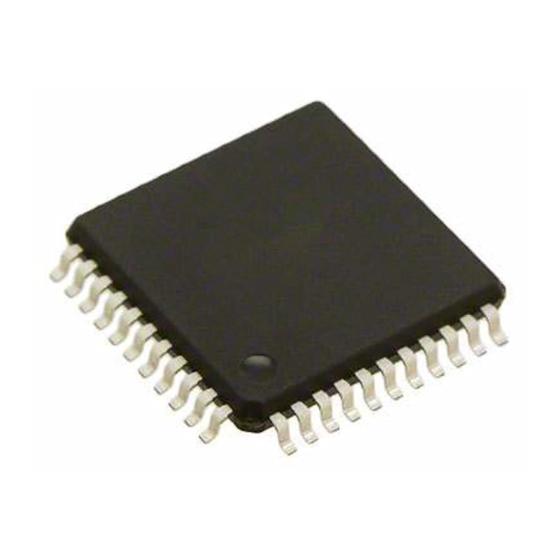
- Page 2 – Two true open-drain output pins – Eight, ultra-high current sink pins supporting 20 mA source/sink current • Package options – 64-pin LQFP; 64-pin QFP – 48-pin LQFP – 44-pin LQFP – 32-pin LQFP MC9S08PA60 Series Data Sheet, Rev. 1, 10/9/2012. Freescale Semiconductor, Inc.
-
Page 3: Table Of Contents
7.1 Obtaining package dimensions.........27 5.1.1 DC characteristics..........7 8 Pinout..................28 5.1.2 Supply current characteristics.......12 8.1 Signal multiplexing and pin assignments......28 5.1.3 EMC performance..........13 8.2 Device pin assignment............31 5.2 Switching specifications.............13 9 Revision history.................34 MC9S08PA60 Series Data Sheet, Rev. 1, 10/9/2012. Freescale Semiconductor, Inc. -
Page 4: Ordering Parts
Approximate flash size in KB • 60 = 60 KB • 32 = 32 KB Temperature range (°C) • V = –40 to 105 Table continues on the next page... MC9S08PA60 Series Data Sheet, Rev. 1, 10/9/2012. Freescale Semiconductor, Inc. -
Page 5: Example
The classification is shown in the column labeled “C” in the parameter tables where appropriate. Ratings 4.1 Thermal handling ratings Symbol Description Min. Max. Unit Notes Storage temperature –55 °C Solder temperature, lead-free — °C MC9S08PA60 Series Data Sheet, Rev. 1, 10/9/2012. Freescale Semiconductor, Inc. -
Page 6: Moisture Handling Ratings
Symbol Description Min. Max. Unit Supply voltage –0.3 Maximum current into V — Digital input voltage (except RESET, EXTAL, and XTAL) –0.3 + 0.3 Table continues on the next page... MC9S08PA60 Series Data Sheet, Rev. 1, 10/9/2012. Freescale Semiconductor, Inc. -
Page 7: General
=20 mA strength 3 V, I — — load Output low Max total I for all — — current ports — — Table continues on the next page... MC9S08PA60 Series Data Sheet, Rev. 1, 10/9/2012. Freescale Semiconductor, Inc. - Page 8 Table 3. LVD and POR Specification Symbol Description Unit POR re-arm voltage 1.75 Falling low-voltage detect LVDH threshold - high range (LVDV = 1) Table continues on the next page... MC9S08PA60 Series Data Sheet, Rev. 1, 10/9/2012. Freescale Semiconductor, Inc.
- Page 9 1. Maximum is highest voltage that POR is guaranteed. 2. Rising thresholds are falling threshold + hysteresis. 3. voltage Factory trimmed at V = 5.0 V, Temp = 25 °C MC9S08PA60 Series Data Sheet, Rev. 1, 10/9/2012. Freescale Semiconductor, Inc.
- Page 10 Nonswitching electrical specifications (mA) Figure 1. Typical I Vs. V (mA) Figure 2. Typical I Vs. V (High current drive) MC9S08PA60 Series Data Sheet, Rev. 1, 10/9/2012. Freescale Semiconductor, Inc.
- Page 11 Nonswitching electrical specifications (mA) Figure 3. Typical I Vs. V (mA) Figure 4. Typical I Vs. V (High current drive) MC9S08PA60 Series Data Sheet, Rev. 1, 10/9/2012. Freescale Semiconductor, Inc.
-
Page 12: Supply Current Characteristics
Stop3 mode supply — — µA -40 to 105 °C current no clocks active — — -40 to 105 °C (except 1 kHz LPO clock) Table continues on the next page... MC9S08PA60 Series Data Sheet, Rev. 1, 10/9/2012. Freescale Semiconductor, Inc. -
Page 13: Emc Performance
BDM modes BKGD/MS hold time after issuing background — — debug force reset to enter user or BDM modes Table continues on the next page... MC9S08PA60 Series Data Sheet, Rev. 1, 10/9/2012. Freescale Semiconductor, Inc. -
Page 14: Debug Trace Timing Specifications
Clock period Frequency dependent Low pulse width — High pulse width — Clock and data rise time — Clock and data fall time — Table continues on the next page... MC9S08PA60 Series Data Sheet, Rev. 1, 10/9/2012. Freescale Semiconductor, Inc. -
Page 15: Ftm Module Timing
Function Symbol Unit External clock TCLK frequency External clock — TCLK period External clock — clkh high time External clock — clkl low time Input capture — ICPW pulse width MC9S08PA60 Series Data Sheet, Rev. 1, 10/9/2012. Freescale Semiconductor, Inc. -
Page 16: Thermal Specifications
Thermal resistance single-layer board θ 64-pin LQFP °C/W θ 64-pin QFP °C/W θ 48-pin LQFP °C/W θ 44-pin LQFP °C/W θ 32-pin LQFP °C/W Table continues on the next page... MC9S08PA60 Series Data Sheet, Rev. 1, 10/9/2012. Freescale Semiconductor, Inc. -
Page 17: Peripheral Operating Requirements And Behaviors
. Using this value of K, the values of P and T be obtained by solving the above equations iteratively for any value of T 6 Peripheral operating requirements and behaviors MC9S08PA60 Series Data Sheet, Rev. 1, 10/9/2012. Freescale Semiconductor, Inc. -
Page 18: External Oscillator (Xosc) And Ics Characteristics
DCO output temperature range from trimmed Over fixed voltage and ±1.0 frequency temperature range of 0 to 70 °C FLL acquisition time — — Acquire Table continues on the next page... MC9S08PA60 Series Data Sheet, Rev. 1, 10/9/2012. Freescale Semiconductor, Inc. -
Page 19: Nvm Specifications
Table 10. Flash characteristics Characteristic Symbol Typical Unit Supply voltage for program/erase -40 °C — prog/erase to 105 °C Supply voltage for read operation — Read Table continues on the next page... MC9S08PA60 Series Data Sheet, Rev. 1, 10/9/2012. Freescale Semiconductor, Inc. -
Page 20: Analog
Program and erase operations do not require any special power sources other than the normal V supply. For more detailed information about program/erase operations, see the Memory section. 6.3 Analog MC9S08PA60 Series Data Sheet, Rev. 1, 10/9/2012. Freescale Semiconductor, Inc. -
Page 21: Adc Characteristics
1. Typical values assume V = 5.0 V, Temp = 25°C, f =1.0 MHz unless otherwise stated. Typical values are for ADCK reference only and are not tested in production. 1. DC potential difference. MC9S08PA60 Series Data Sheet, Rev. 1, 10/9/2012. Freescale Semiconductor, Inc. - Page 22 ADCO = 1 Supply current — µA DDAD ADLPC = 0 ADLSMP = 0 ADCO = 1 Supply current Stop, reset, module — 0.011 µA Table continues on the next page... MC9S08PA60 Series Data Sheet, Rev. 1, 10/9/2012. Freescale Semiconductor, Inc.
- Page 23 2. 1 LSB = (V REFH REFL 3. Monotonicity and no-missing-codes guaranteed in 10-bit and 8-bit modes 3. V ADIN 4. I = leakage current (refer to DC characteristics) MC9S08PA60 Series Data Sheet, Rev. 1, 10/9/2012. Freescale Semiconductor, Inc.
-
Page 24: Analog Comparator (Acmp) Electricals
Data setup time (inputs) — — Data hold time (inputs) — — Data valid (after SPSCK edge) — — Data hold time (outputs) — — Table continues on the next page... MC9S08PA60 Series Data Sheet, Rev. 1, 10/9/2012. Freescale Semiconductor, Inc. - Page 25 (OUTPUT) 1.If configured as output 2. LSBF = 0. For LSBF = 1, bit order is LSB, bit 1, ..., bit 6, MSB. Figure 14. SPI master mode timing (CPHA=1) MC9S08PA60 Series Data Sheet, Rev. 1, 10/9/2012. Freescale Semiconductor, Inc.
- Page 26 SLAVE LSB OUT SLAVE MSB (OUTPUT) note NOTE MOSI BIT 6 . . . 1 MSB IN LSB IN (INPUT) NOTE: Not defined! Figure 15. SPI slave mode timing (CPHA = 0) MC9S08PA60 Series Data Sheet, Rev. 1, 10/9/2012. Freescale Semiconductor, Inc.
-
Page 27: Dimensions
If you want the drawing for this package Then use this document number 32-pin LQFP 98ASH70029A 44-pin LQFP 98ASS23225W 48-pin LQFP 98ASH00962A 64-pin QFP 98ASB42844B 64-pin LQFP 98ASS23234W MC9S08PA60 Series Data Sheet, Rev. 1, 10/9/2012. Freescale Semiconductor, Inc. -
Page 28: Pinout
— PTD5 KBI1P5 — — — PTC1 — FTM2CH1 ADP9 — PTC0 — FTM2CH0 ADP8 — — — — PTF7 — — ADP15 — Table continues on the next page... MC9S08PA60 Series Data Sheet, Rev. 1, 10/9/2012. Freescale Semiconductor, Inc. - Page 29 — PTE1 — MOSI0 — — — PTE0 — SPSCK0 TCLK1 — PTC5 — FTM1CH1 — — PTC4 — FTM1CH0 RTCO — PTA5 TCLK0 — RESET PTA4 — ACMPO BKGD MC9S08PA60 Series Data Sheet, Rev. 1, 10/9/2012. Freescale Semiconductor, Inc.
- Page 30 Disable all modules that share a pin before enabling another module. MC9S08PA60 Series Data Sheet, Rev. 1, 10/9/2012. Freescale Semiconductor, Inc.
-
Page 31: Device Pin Assignment
PTB1/KBI0P5/TxD0/ADP5 Pins in bold are not available on less pi n-count packages. 1. High source/sink current pins 2. True open drain pins Figure 17. MC9S08PA60 64-pin QFP and LQFP package MC9S08PA60 Series Data Sheet, Rev. 1, 10/9/2012. Freescale Semiconductor, Inc. - Page 32 PTB0/KBI0P4/RxD0/ADP4 PTE6 PTB1/KBI0P5/TxD0/ADP5 Pins in bold are not available on less pi n-count packages. 1. High source/sink current pins 2. True open drain pins Figure 18. MC9S08PA60 48-pin LQFP package MC9S08PA60 Series Data Sheet, Rev. 1, 10/9/2012. Freescale Semiconductor, Inc.
- Page 33 PTB6/SDA/XTAL PTB0/KBI0P4/RxD0/ADP4 PTB1/KBI0P5/TxD0/ADP5 Pins in bold are not available on less pi n-count packages. 1. High source/sink current pins 2. True open drain pins Figure 19. MC9S08PA60 44-pin LQFP package MC9S08PA60 Series Data Sheet, Rev. 1, 10/9/2012. Freescale Semiconductor, Inc.
-
Page 34: Revision History
Figure 20. MC9S08PA60 32-pin LQFP package 9 Revision history The following table provides a revision history for this document. Table 17. Revision history Rev. No. Date Substantial Changes 10/2012 Initial public release MC9S08PA60 Series Data Sheet, Rev. 1, 10/9/2012. Freescale Semiconductor, Inc. - Page 35 Freescale Semiconductor assume any liability arising out of the application or use of any USA/Europe or Locations Not Listed: product or circuit, and specifically disclaims any liability, including without limitation Freescale Semiconductor consequential or incidental damages.
Need help?
Do you have a question about the MC9S08PA32 and is the answer not in the manual?
Questions and answers