Table of Contents
Advertisement
Advertisement
Table of Contents

Related Manuals for Texas Instruments CDCE6214-Q1EVM


Summary of Contents for Texas Instruments CDCE6214-Q1EVM
- Page 1 CDCE6214-Q1EVM User's Guide Literature Number: SNAU244 July 2019...
-
Page 2: Table Of Contents
............3.2.1 Use 3.3-V Power Supply and Configure Jumpers ..............3.2.2 Connect SDA, SCL, and GND to USB2ANY ......................Schematic and Layout ........................Schematic ........................Layout Contents SNAU244 – July 2019 Submit Documentation Feedback Copyright © 2019, Texas Instruments Incorporated... -
Page 3: Preface
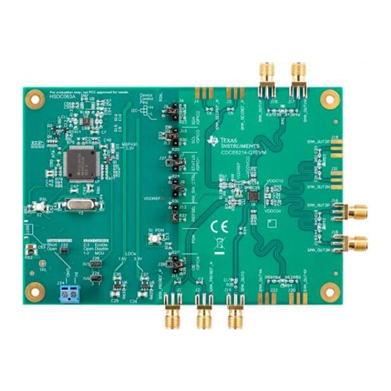
SNAU244 – July 2019 CDCE6214-Q1EVM User's Guide The CDCE6214-Q1EVM is an evaluation platform for the CDCE6214-Q1 automotive Q1-grade, ultra-low power clock generator. This evaluation module uses a USB interface to supply power and program the device. The quick start guide describes the basic configurations the designer can use to start the EVM, and all the different modes of operations are described in subsequent sections. -
Page 4: Quick Start
If the connection mode stays red, follow the instructions listed in Section 3.1 Figure 1-1. TICS Pro Snapshot With USB2ANY Connected Quick Start SNAU244 – July 2019 Submit Documentation Feedback Copyright © 2019, Texas Instruments Incorporated... -
Page 5: Configure Jumpers
5. Remove all other jumpers or leave them floating by connecting them to only one pin. The position of J25 is not important because the resistors required to enable a 3.3-V rail are not populated by default. Figure 1-2. Jumper Configuration Guideline SNAU244 – July 2019 Quick Start Submit Documentation Feedback Copyright © 2019, Texas Instruments Incorporated... -
Page 6: Scan I2C Bus
Click the "Scan I2C Bus" in the small toolbar. Look for the "Device found at 0x68. Address will be updated." text in the message window. Figure 1-3. Scan I2C Bus Quick Start SNAU244 – July 2019 Submit Documentation Feedback Copyright © 2019, Texas Instruments Incorporated... -
Page 7: Load Default And Check Lock Status
"Recalibrate" button, then "Check Lock Status". Watch for the green "locked" text to confirm that the PLL is locked. Figure 1-4. Check Lock Status SNAU244 – July 2019 Quick Start Submit Documentation Feedback Copyright © 2019, Texas Instruments Incorporated... -
Page 8: Check Outputs
The other pins can only be configured by the on-board jumpers or connected to an external controller. They cannot be controlled by TICS Pro. Figure 1-5. Configure Outputs Quick Start SNAU244 – July 2019 Submit Documentation Feedback Copyright © 2019, Texas Instruments Incorporated... -
Page 9: Modes Of Operations
SMA connectors J1 and/or J2. For the secondary reference, if crystal input is preferred, refer to Section 2.1.2. Otherwise, populate C5. R7, C6, R11, J3, J4 and feed reference source from SMA connectors J3 and/or J4. SNAU244 – July 2019 Modes of Operations Submit Documentation Feedback Copyright © 2019, Texas Instruments Incorporated... -
Page 10: Crystal Input
Output Configuration On the TICS Pro "Outputs" page, the designer can program output channel MUX, integer output divider values, as well as output format. Modes of Operations SNAU244 – July 2019 Submit Documentation Feedback Copyright © 2019, Texas Instruments Incorporated... -
Page 11: V And 3.3-V Power Supply
J25. To disable the 3.3-V LDOs, remove the jumper for J25. WARNING Do NOT enable 1.8-V and 3.3-V LDOs at the same time. Figure 2-2. Board Rework Guide to Enable 3.3-V Supply SNAU244 – July 2019 Modes of Operations Submit Documentation Feedback Copyright © 2019, Texas Instruments Incorporated... -
Page 12: Frequently Asked Questions - Faq
Note that the firmware loader only works on Windows 7 or lower versions of Windows system. The firmware does not work on the Windows 10 system at the time of this user manual publication. Frequently Asked Questions - FAQ SNAU244 – July 2019 Submit Documentation Feedback Copyright © 2019, Texas Instruments Incorporated... -
Page 13: How To Use External Microcontroller
J10), and GND to USB2ANY. Refer to Figure 3-2 for details on how to connect these three wires to USB2ANY. Figure 3-2. EVM Blue Wire Guide SNAU244 – July 2019 Frequently Asked Questions - FAQ Submit Documentation Feedback Copyright © 2019, Texas Instruments Incorporated... -
Page 14: Connect Sda, Scl, And Gnd To Usb2Any
SDA, SCL and GND to pin 1, pin 2, and pin 5 of USB2ANY (J4 in Figure 3-3) separately. The rectangle on the top indicates the slot of USB2ANY box. Figure 3-3. USB2ANY Pin Connection Frequently Asked Questions - FAQ SNAU244 – July 2019 Submit Documentation Feedback Copyright © 2019, Texas Instruments Incorporated... -
Page 15: Schematic And Layout
Chapter 4 SNAU244 – July 2019 Schematic and Layout Schematic Figure 4-1. Schematic Page 1: Cover Sheet SNAU244 – July 2019 Schematic and Layout Submit Documentation Feedback Copyright © 2019, Texas Instruments Incorporated... - Page 16 Schematic www.ti.com Figure 4-2. Schematic Page 2: USB Schematic and Layout SNAU244 – July 2019 Submit Documentation Feedback Copyright © 2019, Texas Instruments Incorporated...
- Page 17 Schematic www.ti.com Figure 4-3. Schematic Page 3: Power SNAU244 – July 2019 Schematic and Layout Submit Documentation Feedback Copyright © 2019, Texas Instruments Incorporated...
- Page 18 Schematic www.ti.com Figure 4-4. Schematic Page 4: Power Filter Distribution Schematic and Layout SNAU244 – July 2019 Submit Documentation Feedback Copyright © 2019, Texas Instruments Incorporated...
- Page 19 Schematic www.ti.com Figure 4-5. Schematic Page 5: Level Shifter SNAU244 – July 2019 Schematic and Layout Submit Documentation Feedback Copyright © 2019, Texas Instruments Incorporated...
- Page 20 Schematic www.ti.com Figure 4-6. Schematic Page 6: Input and Clock Generator Schematic and Layout SNAU244 – July 2019 Submit Documentation Feedback Copyright © 2019, Texas Instruments Incorporated...
- Page 21 Schematic www.ti.com Figure 4-7. Schematic Page 7: Outputs SNAU244 – July 2019 Schematic and Layout Submit Documentation Feedback Copyright © 2019, Texas Instruments Incorporated...
- Page 22 Schematic www.ti.com Figure 4-8. Schematic Page 8: EVM Hardware Schematic and Layout SNAU244 – July 2019 Submit Documentation Feedback Copyright © 2019, Texas Instruments Incorporated...
-
Page 23: Layout
Layout www.ti.com Layout Figure 4-9. PCB Layer 1: Top Layer Composite SNAU244 – July 2019 Schematic and Layout Submit Documentation Feedback Copyright © 2019, Texas Instruments Incorporated... - Page 24 Layout www.ti.com Figure 4-10. PCB Layer 2: Middle Layer Schematic and Layout SNAU244 – July 2019 Submit Documentation Feedback Copyright © 2019, Texas Instruments Incorporated...
- Page 25 Layout www.ti.com Figure 4-11. PCB Layer 3: Middle Layer SNAU244 – July 2019 Schematic and Layout Submit Documentation Feedback Copyright © 2019, Texas Instruments Incorporated...
- Page 26 Layout www.ti.com Figure 4-12. PCB Layer 4: Bottom Layer Composite Schematic and Layout SNAU244 – July 2019 Submit Documentation Feedback Copyright © 2019, Texas Instruments Incorporated...
- Page 27 TI products. TI’s provision of these resources does not expand or otherwise alter TI’s applicable warranties or warranty disclaimers for TI products. Mailing Address: Texas Instruments, Post Office Box 655303, Dallas, Texas 75265 Copyright © 2019, Texas Instruments Incorporated...
Need help?
Do you have a question about the CDCE6214-Q1EVM and is the answer not in the manual?
Questions and answers