Advertisement
Quick Links
Low Phase Noise Clock Evaluation Module — up to 1.5
1
Features
• Easy-to-use evaluation module to generate low
phase noise clocks up to 1.5 GHz
• Easy device programming via host-powered USB
port
• Rapid configuration through provided EVM Control
Software
• Can be powered from the USB port, or by an
external 3.3V power supply
• Single-ended or differential input; external crystal
can be used with on-chip oscillator
• Footprint for optional crystal filter on one output
2
General Description
The CDCE62005 is a high performance, low phase noise frequency synthesizer and jitter cleaner. It
features an on-chip PLL with dual integrated LC Voltage Controlled Oscillators (VCOs) operating from
1.75–2.35 GHz. It provides support for three manually or automatically selected inputs, and provides up to
five differential, or ten single-ended, low-jitter outputs.
The CDCE62005 supports single-ended and differential input signals, as well as providing a crystal
oscillator circuit that operates in conjunction with an external AT-cut crystal.
The CDCE62005 is programmed through an SPI interface using the supplied EVM programming graphical
user interface (GUI).
The evaluation module (EVM) demonstrates the electrical performance of the device. This
fully-assembled, factory-tested evaluation board allows complete validation of all device functions. For
optimum performance, the board is equipped with 50Ω SMA connectors and well-controlled 50Ω
impedance microstrip transmission lines.
3
Signal Path and Control
The CDCE62005 provides three selectable inputs – PRI REF, SEC REF, and AUX IN. The PRI REF and
SEC REF inputs can accept up to 1500 MHz in the fan-out mode. In the PLL mode, PRI REF and SEC
REF can accept an input at up to 500MHz from a differential signal source, or up to 250MHz from a single
SCAU024 – September 2008
Submit Documentation Feedback
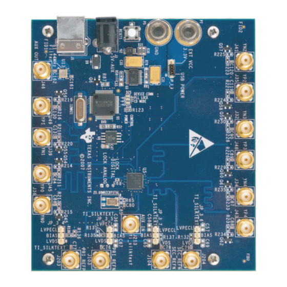
Figure 1. CDCE62005EVM Evaluation Board
Low Phase Noise Clock Evaluation Module — up to 1.5 GHz
User's Guide
SCAU024 – September 2008
GHz
1
Advertisement

Related Manuals for Texas Instruments CDCE62005


Summary of Contents for Texas Instruments CDCE62005
- Page 1 Signal Path and Control The CDCE62005 provides three selectable inputs – PRI REF, SEC REF, and AUX IN. The PRI REF and SEC REF inputs can accept up to 1500 MHz in the fan-out mode. In the PLL mode, PRI REF and SEC REF can accept an input at up to 500MHz from a differential signal source, or up to 250MHz from a single SCAU024 –...
- Page 2 The CDCE62005 can use either a completely-internal loop filter, or a partially-external loop filter. The loop-filter selection will affect the phase noise and loop stability of the PLL. If the CDCE62005 is to be used only as a frequency synthesizer, the completely internal loop filter option is recommended. If the...
- Page 3 Installing the EVM Control Software and USB Driver www.ti.com Connect the USB cable to the EVM. If a box appears asking for an appropriate driver, Do not use the automatic search option! Select a manual installation and when prompted for the driver location browse to the CDCE62005EVM program file folder that was used during instillation.
- Page 4 Figure 2. TI CDCE62005 EVMCS Display Using the EVM Control Software The graphical layout of the EVMCS is based on the functional structure of the CDCE62005. Using the EVMCS, the system designer can change the Input Frequency, Input Divider, Input type, Input selection, PFD Charge Pump, Internal/External Loop Filter, Output MUX selection, Output Divider, and Output type.
- Page 5 Figure 3, showing selections on the external input signal type (differential or single ended), the external signal connection to the CDCE62005 primary/secondary inputs (AC or DC termination), input-buffer internal termination (enabled or disabled), and the input-buffer VBB voltage polarity (normal or inverted).
- Page 6 Installing the EVM Control Software and USB Driver www.ti.com The PFD and Charge Pump section of the EVMCS can be clicked for a popup window that opens, as shown in Figure 5, showing selections for the charge pump current and charge pump pulse width. For the internal loop filter, lower charge pump currents work well and for the external loop filter, higher charge pump currents work well.
- Page 7 Installing the EVM Control Software and USB Driver www.ti.com Figure 7. Loop Filter, Additional External Components 5. Output MUX Selection The Output MUX section of the EVMCS for each of the five outputs can be clicked to open a popup window, shown in Figure 8, showing each Output MUX clock source.
- Page 8 EXT VDD and GND. In this configuration the USB microcontroller is powered by the USB port 5V supply, while the CDCE62005 is powered by the 3.3V external supply. This configuration is best for programming the CDCE62005 while also taking measurements. This configuration removes the power variation found in USB power supplies by isolating the CDCE62005 from the USB supply.
- Page 9 Configuration for On-board External Loop Filter If the CDCE62005 is configured as a jitter cleaner, it requires the use of the partially-external loop filter, located on the bottom side of the CDCE62005EVM PC board. There are four external loop filter options provided on the EVM.
- Page 10 CDCE62005EVM Board Schematic Diagram www.ti.com CDCE62005EVM Board Schematic Diagram Low Phase Noise Clock Evaluation Module — up to 1.5 GHz SCAU024 – September 2008 Submit Documentation Feedback...
- Page 11 CDCE62005EVM Board Schematic Diagram www.ti.com SCAU024 – September 2008 Low Phase Noise Clock Evaluation Module — up to 1.5 GHz Submit Documentation Feedback...
- Page 12 CDCE62005EVM Board Schematic Diagram www.ti.com Low Phase Noise Clock Evaluation Module — up to 1.5 GHz SCAU024 – September 2008 Submit Documentation Feedback...
- Page 13 CDCE62005EVM Board Schematic Diagram www.ti.com SCAU024 – September 2008 Low Phase Noise Clock Evaluation Module — up to 1.5 GHz Submit Documentation Feedback...
- Page 14 CDCE62005EVM Board Schematic Diagram www.ti.com Low Phase Noise Clock Evaluation Module — up to 1.5 GHz SCAU024 – September 2008 Submit Documentation Feedback...
-
Page 15: Evaluation Board/Kit Important Notice
EVALUATION BOARD/KIT IMPORTANT NOTICE Texas Instruments (TI) provides the enclosed product(s) under the following conditions: This evaluation board/kit is intended for use for ENGINEERING DEVELOPMENT, DEMONSTRATION, OR EVALUATION PURPOSES ONLY and is not considered by TI to be a finished end-product fit for general consumer use. Persons handling the product(s) must have electronics training and observe good engineering practice standards. - Page 16 CDCE62005EVM Board Schematic Diagram www.ti.com EVM WARNINGS AND RESTRICTIONS It is important to operate this EVM within the input voltage range of 3 V to 3.6 V and the output voltage range of 0 V to 3.6 V. Exceeding the specified input range may cause unexpected operation and/or irreversible damage to the EVM. If there are questions concerning the input range, please contact a TI field representative prior to connecting the input power.
-
Page 17: Important Notice
IMPORTANT NOTICE Texas Instruments Incorporated and its subsidiaries (TI) reserve the right to make corrections, modifications, enhancements, improvements, and other changes to its products and services at any time and to discontinue any product or service without notice. Customers should obtain the latest relevant information before placing orders and should verify that such information is current and complete. - Page 18 Mouser Electronics Authorized Distributor Click to View Pricing, Inventory, Delivery & Lifecycle Information: Texas Instruments CDCE62005EVM...
Need help?
Do you have a question about the CDCE62005 and is the answer not in the manual?
Questions and answers