Advertisement
Quick Links
www.ti.com
EVM User's Guide: CDC6CEVM
CDC6CEVM User's Guide
1 Description
The CDC6EVM provides a complete evaluation
platform to evaluate the clock performance and
flexibility of the Texas Instruments CDC6C low power,
LVCMOS BAW Oscillator family. This EVM can be
used as a flexible clock source for compliance
testing, performance evaluation, and initial system
prototyping. The onboard edge-launch SMA ports
provide access to the configurable clock output of the
CDC6C, which allows the device to interface with test
equipment and reference boards using commercially
available coaxial cables, adapters, or baluns (not
included).
SNAU286 – NOVEMBER 2024
Submit Document Feedback
2 Features
•
Contains footprints for four standard LVCMOS
oscillator packages: DLE/DLN (3.2mm × 2.5mm),
DLF (2.5mm × 2.0mm), DLX/DLR (2.0mm ×
1.6mm), and DLY (1.6mm × 1.2mm)
•
Onboard voltage regulators to generate standard
supply voltages (1.8V, 2.5V, 3.3V)
•
Can be powered using USB only, option for
external power supply
CDC6CEVM Evaluation Board
Copyright © 2024 Texas Instruments Incorporated
Description
CDC6CEVM User's Guide
1
Advertisement

Related Manuals for Texas Instruments CDC6CEVM


Summary of Contents for Texas Instruments CDC6CEVM
- Page 1 Contains footprints for four standard LVCMOS platform to evaluate the clock performance and oscillator packages: DLE/DLN (3.2mm × 2.5mm), flexibility of the Texas Instruments CDC6C low power, DLF (2.5mm × 2.0mm), DLX/DLR (2.0mm × LVCMOS BAW Oscillator family. This EVM can be 1.6mm), and DLY (1.6mm ×...
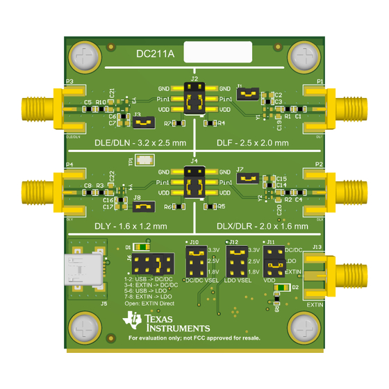
- Page 2 1.6mm), and DLY (1.6mm × 1.2mm). All four footprints are included on the EVM with independent termination networks. By default the CDC6CEVM is populated with a 25MHz variant of CDC6C with a DLE package size. The DLF, DLX, and DLY footprints are left unpopulated by default so the user can solder the desired frequency variant for evaluation.
- Page 3 4.2.1 Connection Diagram Figure 4-1 shows the CDC6CEVM (DCC211A) connection diagram. The top region of the board contains 4 quadrants, one for each package size. Each quadrant contains a footprint to populate a CDC6C oscillator (Y1, Y2, Y3, Y4), a jumper to pull the OE pin high or low (J2, J4), and an output termination network with an SMA connector (P1, P2, P3, P4).
- Page 4 Pull CDC6C DLY (Y4) OE to GND VDD_DLF DLF VDD Supply Tie pins 1-2 (default): Connect VDD to CDC6C DLF (Y1) Leave open: Disconnect VDD from CDC6C DLF (Y1) CDC6CEVM User's Guide SNAU286 – NOVEMBER 2024 Submit Document Feedback Copyright © 2024 Texas Instruments Incorporated...
- Page 5 Disconnect VDD from CDC6C DLY (Y4) 4.2.5 Configuring the Output Clock Termination The CDC6CEVM comes pre-populated with an AC-coupled LVCMOS termination. The termination can be modified to support either an AC-coupled or a DC-coupled LVCMOS output format. To switch the Y1, Y2, Y3, or Y4 formats to DC-coupled, replace C1, C5, C4, and C8, respectively, with 0-ohm resistors.
- Page 6 Implementation Results www.ti.com 4.3 Performance Data and Results 4.3.1 Typical Measurement Figure 4-2. Phase Noise Plot of 25MHz CDC6C Variant CDC6CEVM User's Guide SNAU286 – NOVEMBER 2024 Submit Document Feedback Copyright © 2024 Texas Instruments Incorporated...
- Page 7 Figure 4-3. Oscilloscope Waveform of 25MHz CDC6C Variant The output amplitude is reduced from 3.3V to around 1.75V due to the internal 50Ω termination of the oscilloscope SNAU286 – NOVEMBER 2024 CDC6CEVM User's Guide Submit Document Feedback Copyright © 2024 Texas Instruments Incorporated...
- Page 8 P in1_DL Y OE/ST/NC OE/ST/NC CDC6CE025000ADLET CDC6CXXXXXXXDL YT CDC6CDLE/DLN - 3.2 x 2.5 mm CDC6CDLY - 1.6 x 1.2 mm Figure 5-1. Schematic - CDC6C Oscillators CDC6CEVM User's Guide SNAU286 – NOVEMBER 2024 Submit Document Feedback Copyright © 2024 Texas Instruments Incorporated...
- Page 9 J 23: S e le cts power s upply type for VDDO Figure 5-2. Schematic - Power Supply 5.2 PCB Layout and Layer Stack-Up 5.2.1 PCB Layer Stack-Up Figure 5-3. PCB Layer Stack-Up SNAU286 – NOVEMBER 2024 CDC6CEVM User's Guide Submit Document Feedback Copyright © 2024 Texas Instruments Incorporated...
- Page 10 Hardware Design Files www.ti.com 5.2.2 PCB Layout Figure 5-4. Top View Composite Figure 5-5. Top Layer Figure 5-6. GND Layer Figure 5-7. PWR Layer CDC6CEVM User's Guide SNAU286 – NOVEMBER 2024 Submit Document Feedback Copyright © 2024 Texas Instruments Incorporated...
- Page 11 Sullins Connector J2, J4 Header, 2.54mm, 3x2, Gold, Black, SMT GBC03DABN-M30 Solutions Connector, Receptacle, Mini-USB Type B, R/A, Top Mount SMT 1734035-2 TE Connectivity SNAU286 – NOVEMBER 2024 CDC6CEVM User's Guide Submit Document Feedback Copyright © 2024 Texas Instruments Incorporated...
- Page 12 Automotive 1-Channel ESD in 0402 Package With 10pF TPD1E10B09QDPY Texas Instruments Capacitance and 9V Breakdown, DPY0002A (X1SON-2) 600-mA, Ultra-Low IQ Step-Down Converter, YKA0006ACAC TPS62808YKAR Texas Instruments (DSBGA-6) CDC6CEVM User's Guide SNAU286 – NOVEMBER 2024 Submit Document Feedback Copyright © 2024 Texas Instruments Incorporated...
- Page 13 All trademarks are the property of their respective owners. 7 Related Documentation See the CDC6Cx Low Power LVCMOS output BAW Oscillator Data Sheet for more information about the CDC6C devices. SNAU286 – NOVEMBER 2024 CDC6CEVM User's Guide Submit Document Feedback Copyright © 2024 Texas Instruments Incorporated...
- Page 14 STANDARD TERMS FOR EVALUATION MODULES Delivery: TI delivers TI evaluation boards, kits, or modules, including any accompanying demonstration software, components, and/or documentation which may be provided together or separately (collectively, an “EVM” or “EVMs”) to the User (“User”) in accordance with the terms set forth herein.
- Page 15 www.ti.com Regulatory Notices: 3.1 United States 3.1.1 Notice applicable to EVMs not FCC-Approved: FCC NOTICE: This kit is designed to allow product developers to evaluate electronic components, circuitry, or software associated with the kit to determine whether to incorporate such items in a finished product and software developers to write software applications for use with the end product.
- Page 16 www.ti.com Concernant les EVMs avec antennes détachables Conformément à la réglementation d'Industrie Canada, le présent émetteur radio peut fonctionner avec une antenne d'un type et d'un gain maximal (ou inférieur) approuvé pour l'émetteur par Industrie Canada. Dans le but de réduire les risques de brouillage radioélectrique à...
- Page 17 www.ti.com EVM Use Restrictions and Warnings: 4.1 EVMS ARE NOT FOR USE IN FUNCTIONAL SAFETY AND/OR SAFETY CRITICAL EVALUATIONS, INCLUDING BUT NOT LIMITED TO EVALUATIONS OF LIFE SUPPORT APPLICATIONS. 4.2 User must read and apply the user guide and other available documentation provided by TI regarding the EVM prior to handling or using the EVM, including without limitation any warning or restriction notices.
- Page 18 Notwithstanding the foregoing, any judgment may be enforced in any United States or foreign court, and TI may seek injunctive relief in any United States or foreign court. Mailing Address: Texas Instruments, Post Office Box 655303, Dallas, Texas 75265 Copyright © 2023, Texas Instruments Incorporated...
- Page 19 TI products. TI’s provision of these resources does not expand or otherwise alter TI’s applicable warranties or warranty disclaimers for TI products. TI objects to and rejects any additional or different terms you may have proposed. IMPORTANT NOTICE Mailing Address: Texas Instruments, Post Office Box 655303, Dallas, Texas 75265 Copyright © 2024, Texas Instruments Incorporated...
Need help?
Do you have a question about the CDC6CEVM and is the answer not in the manual?
Questions and answers