Table of Contents
Advertisement
Quick Links
1.5-GHz Low-Phase Noise Clock Evaluation Board
This user's guide discusses the general operation and configuration of the Texas Instruments CDCE72010
evaluation board.
.......................................................................................................................
1
2
3
4
5
6
7
7.1
8
8.1
8.2
8.3
8.4
8.5
9
1
2
CDCE72010EVM External Loop Filter Topology
Windows is a trademark of Microsoft Corporartion.
SLAU250 - May 2008
Submit Documentation Feedback
Contents
.........................................................................................................
.........................................................................................
..............................................................................................
.............................................................................
.......................................................................................
....................................................................................
..........................................................................
.....................................................................................................
.......................................................................................................
..............................................................................
..........................................................................
List of Figures
....................................................................................................
.......................................................................
..................................................
...............................................................
1.5-GHz Low-Phase Noise Clock Evaluation Board
User's Guide
SLAU250 - May 2008
2
2
3
3
3
5
5
5
10
..........................
10
10
10
11
12
13
2
12
1
Advertisement
Table of Contents

Related Manuals for Texas Instruments CDCE72010


Summary of Contents for Texas Instruments CDCE72010
-
Page 1: Table Of Contents
User's Guide SLAU250 – May 2008 1.5-GHz Low-Phase Noise Clock Evaluation Board This user's guide discusses the general operation and configuration of the Texas Instruments CDCE72010 evaluation board. Contents ........................Features ......................General Description ..................Signal Path and Control Circuitry .................... -
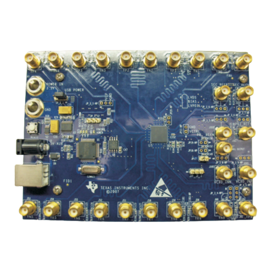
Page 2: Features
Figure 1. CDCE72010EVM Board General Description The CDCE72010 is a high-performance, low-phase noise clock synchronizer and jitter cleaner. It has one main universal VCO/VCXO input buffer and an auxiliary universal input buffer. Either Input can drive the outputs and/or the feedback path to the PFD. The maximum VCXO/VCO input frequency is 1.5 GHz. It provides support for two redundant input references and using its on-chip PLL architecture can provide up to ten differential or 20 single-ended low jitter outputs. -
Page 3: Signal Path And Control Circuitry
Signal Path and Control Circuitry The CDCE72010 provides support for selectable tri-inputs, and two of the inputs (PRI REF and SEC REF) can accept a 8-kHz to 500-MHz frequency input from a differential signal source or a 8-kHz to 200-MHz frequency input from a single-ended signal source. - Page 4 Select a manual installation, and when prompted for the driver location, browse to the CDCE72010 GUI file folder that was used during instillation. If the Windows operating system does not ask for a driver, no action is required.
-
Page 5: Cdce72010 Control Gui Interface
Divider, and Output type. The rest are selected by the software with user-selectable options as described in the steps below. If the power to the CDCE72010 is derived from the USB, the Enable EVM Power button needs to be checked. If the power to the CDCE72010 is derived from an external source, the Enable EVM Power button needs to be unchecked. - Page 6 Before programming the PLL, select the External Control Pins button in the EVM Status section of the GUI. The selections on this popup window, as shown in the following illustration, must be selected according to the desired working configuration of the CDCE72010. 1.5-GHz Low-Phase Noise Clock Evaluation Board SLAU250 –...
- Page 7 This illustration shows selections on the external input signal type (differential or single ended), the external signal connection to the CDCE72010 primary/secondary inputs (AC or DC termination), input buffer internal termination (enabled or disabled), input buffer VBB voltage polarity (normal or inverted), input buffer hysteresis, and fail-safe mode (enabled or disabled).
- Page 8 Step 5: Output Divider The CDCE72010 has 10 outputs and 8 Output Dividers. Outputs 0 and 1 share the same divider, and outputs 8 and 9 share the same divider. The Output Divider and the Output Phase Adjust are accessed by clicking on the divider needed.
- Page 9 Either CMOS output can be active, inverting, tri-state or low. Each output can be independently disabled. Step 7: Write to CDCE72010 EEPROM To write any particular setting to the EEPROM (locked or unlocked), the menu item at the top of the GUI entitled Tool must be clicked which reveals the items Write EEPROM Unlocked and Write EEPROM Locked as part of a drop-down menu.
-
Page 10: Configuring The Board
When operating the CDCE72010 without the USB programming cable (useful in laboratory settings in which a PC is unavailable at the laboratory station), the CDCE72010 needs to be configured and saved in the EEPROM in one of the preceding configurations and then reconfigured for external power supply usage. -
Page 11: Configuration For Onboard External Loop Filter
Configuration for Onboard External Loop Filter If the CDCE72010 is chosen to be operated as a jitter cleaner, it requires use of the partially external loop filter which is located at the back side of the CDCE72010EVM. The EVM provides four external loop filter options. -
Page 12: Configuration For Pll Lock Detect
Configuration for PLL Lock Detect The CDCE72010 PLL lock detect can be chosen on the CDCE72010EVM as either an analog lock detect or a digital lock detect using the jumper, JP_3_12, located at the back side of the CDCE72010EVM. This jumper can be configured as shown in the following diagram for either analog or digital lock detect. -
Page 13: Cdce72010Evm Board Schematic Diagram
CDCE72010EVM Board Schematic Diagram www.ti.com CDCE72010EVM Board Schematic Diagram SLAU250 – May 2008 1.5-GHz Low-Phase Noise Clock Evaluation Board Submit Documentation Feedback... - Page 14 CDCE72010EVM Board Schematic Diagram www.ti.com 1.5-GHz Low-Phase Noise Clock Evaluation Board SLAU250 – May 2008 Submit Documentation Feedback...
- Page 15 CDCE72010EVM Board Schematic Diagram www.ti.com SLAU250 – May 2008 1.5-GHz Low-Phase Noise Clock Evaluation Board Submit Documentation Feedback...
- Page 16 CDCE72010EVM Board Schematic Diagram www.ti.com 1.5-GHz Low-Phase Noise Clock Evaluation Board SLAU250 – May 2008 Submit Documentation Feedback...
- Page 17 CDCE72010EVM Board Schematic Diagram www.ti.com SLAU250 – May 2008 1.5-GHz Low-Phase Noise Clock Evaluation Board Submit Documentation Feedback...
- Page 18 CDCE72010EVM Board Schematic Diagram www.ti.com 1.5-GHz Low-Phase Noise Clock Evaluation Board SLAU250 – May 2008 Submit Documentation Feedback...
- Page 19 EVALUATION BOARD/KIT IMPORTANT NOTICE Texas Instruments (TI) provides the enclosed product(s) under the following conditions: This evaluation board/kit is intended for use for ENGINEERING DEVELOPMENT, DEMONSTRATION, OR EVALUATION PURPOSES ONLY and is not considered by TI to be a finished end-product fit for general consumer use. Persons handling the product(s) must have electronics training and observe good engineering practice standards.
- Page 20 IMPORTANT NOTICE Texas Instruments Incorporated and its subsidiaries (TI) reserve the right to make corrections, modifications, enhancements, improvements, and other changes to its products and services at any time and to discontinue any product or service without notice. Customers should obtain the latest relevant information before placing orders and should verify that such information is current and complete.
Need help?
Do you have a question about the CDCE72010 and is the answer not in the manual?
Questions and answers