
Related Manuals for Aaeon BOXER-6616


Summary of Contents for Aaeon BOXER-6616
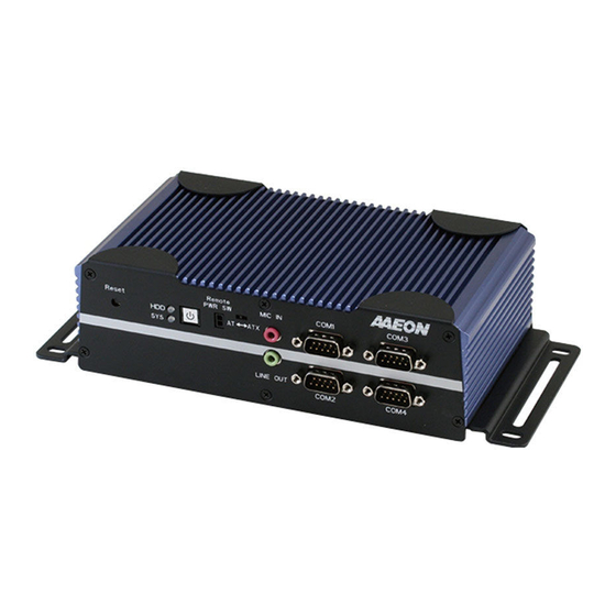
- Page 1 BOXER-6616 Fanless Embedded Box PC User’s Manual 1 Last Updated: July 11, 2017...
- Page 2 AAEON assumes no liabilities resulting from errors or omissions in this document, or from the use of the information contained herein. AAEON reserves the right to make changes in the product design without notice to its users.
- Page 3 Acknowledgement All other products’ name or trademarks are properties of their respective owners. Microsoft Windows ® is a registered trademark of Microsoft Corp. Intel , Platium , Celeron , and Xeon are registered trademarks of Intel ® ® ® ®...
- Page 4 Packing List Before setting up your product, please make sure the following items have been shipped: Item Quantity BOXER-6616 Wallmount bracket Screw Package Phoenix power connector Product DVD with User’s Manual (in pdf) and drivers ...
- Page 5 (if any), its specifications, dimensions, jumper/connector settings/definitions, and driver installation instructions (if any), to facilitate users in setting up their product. Users may refer to the AAEON.com for the latest version of this document. Preface...
- Page 6 Safety Precautions Please read the following safety instructions carefully. It is advised that you keep this manual for future references All cautions and warnings on the device should be noted. Make sure the power source matches the power rating of the device. Position the power cord so that people cannot step on it.
- Page 7 Do NOT disassemble the motherboard so as not to damage the system or void your warranty. If the thermal pad had been damaged, please contact AAEON's salesperson to purchase a new one. Do NOT use those of other brands. The Hex Cylinder Coppers on the front panel are not removable.
- Page 8 FCC Statement This device complies with Part 15 FCC Rules. Operation is subject to the following two conditions: (1) this device may not cause harmful interference, and (2) this device must accept any interference received including interference that may cause undesired operation. Caution: There is a danger of explosion if the battery is incorrectly replaced.
- Page 9 China RoHS Requirements (CN) 产品中有毒有害物质或元素名称及含量 AAEON Embedded Box PC/ Industrial System 有毒有害物质或元素 部件名称 铅 汞 镉 六价铬 多溴联苯 多溴二苯醚 (Pb) (Hg) (Cd) (Cr(VI)) (PBB) (PBDE) 印刷电路板 ○ ○ ○ ○ ○ ○ 及其电子组件 外部信号 ○ ○ ○ ○ ○ ○...
- Page 10 China RoHS Requirement (EN) Poisonous or Hazardous Substances or Elements in Products AAEON Embedded Box PC/ Industrial System Poisonous or Hazardous Substances or Elements Hexavalent Polybrominated Polybrominated Component Lead Mercury Cadmium Chromium Biphenyls Diphenyl Ethers (Pb) (Hg) (Cd) (Cr(VI)) (PBB) (PBDE) PCB &...
-
Page 11: Table Of Contents
Table of Contents Chapter 1 - Product Specifications ..................1 Specifications ......................2 Chapter 2 – Hardware Information ..................4 Dimensions ......................5 Jumpers and Connectors ..................6 Block Diagram ......................7 List of Jumpers ......................8 2.4.1 Clear CMOS Jumper (JP1) ..............8 2.4.2 LVDS Power &... - Page 12 2.5.12 LPC Port (CN24) ..................23 2.5.13 Mini-Card Slot (Half-Mini Card) (CN37) ........... 23 2.5.14 LAN1/USB3x2 (CN40)................26 2.5.15 LAN2/USB3x2 (CN41)................27 2.5.16 Digital IO Port (CN43) ................28 2.5.17 DDR3L SO-DIMM Slot (DIMM1) ............29 2.5.18 VGA\HDMI Port (CN53) ..............29 2.5.19 COM Port1/2 (COM1) ................
- Page 13 3.4.4.6 SIO Configuration: Serial Port 6 Configuration ..... 58 3.4.5 Power Management ................59 3.4.6 Advanced: Dynamic Digital IO Configuration ........ 60 Setup submenu: Chipset..................61 3.5.1 Chipset: North Bridge ................62 3.5.2 Chipset: South Bridge ................63 Setup submenu: Security ..................64 Setup submenu: Boot ..................
-
Page 14: Chapter 1 - Product Specifications
Chapter 1 Chapter 1 - Product Specifications... -
Page 15: Specifications
Specifications System Intel (R) Pentium(R) N4200 2.5GHz or Processor Celeron(R) N3350 2.4GHz Intel® System on Chip Chipset 204-pin 1866 DDR3L SODIMM x 1, up to System Memory VGA x 1 Display Interface HDMI x 1 mSATA, 2.5” HDD/SSD Storage Device ... - Page 16 Power LED x 1 Indicator HDD Active LED x 1 Windows® 10 OS Support Win10 IOT Linux Mechanical Wallmount Mounting DIN Rail (optional) 197mm x 111mm x 61.2mm Dimension (W x H x D) Gross Weight ...
-
Page 17: Chapter 2 - Hardware Information
Chapter 2 Chapter 2 – Hardware Information... -
Page 18: Dimensions
Dimensions Chapter 2 – Hardware Information... -
Page 19: Jumpers And Connectors
Jumpers and Connectors Chapter 2 – Hardware Information... -
Page 20: Block Diagram
Block Diagram Chapter 2 – Hardware Information... -
Page 21: List Of Jumpers
List of Jumpers Please refer to the table below for all of the system’s jumpers that you can configure for your application. Label Function Clear CMOS Jumper LVDS Power & Backlight Power Selection LVDS Backlight Control Selection Touch Screen Lines 4,5,8 Wire Selection COM2 Pin18 Function Selection COM2 Pin9 Function Selection JP11... -
Page 22: Lvds Bklt Control Selection (Jp4)
2.4.3 LVDS BKLT Control Selection (JP4) VR Mode(Default) PWM Mode 2.4.4 Touch Screen Lines 4, 5, 8 Wire Selection (JP5) 4, 8 wire (Default) 5 wire 2.4.5 COM2A Pin18 Function Selection (JP7) +12V Ring (Default) 2.4.6 COM2B Pin9 Function Selection (JP8) +12V Ring (Default) Chapter 2 –... -
Page 23: Front Panel (Jp11)
2.4.7 Front Panel (JP11) Function EXT_PWRBTN# FP_HDLED- FP_HDLED+ FP_SPKR- +V5S PWRLED+ HWRST# Chapter 2 – Hardware Information... -
Page 24: List Of Connectors
List of Connectors Please refer to the table below for all of the system’s connectors that you can configure for your application Label Function RTC Battery External Power Input LVDS Backlight LVDS CN13 UIM Card push-push (Optional) CN14 SATA HDD CN15 +5V/+12V Output for SATA HDD CN16... - Page 25 Label Function COM3 COM Port 5/6 Chapter 2 – Hardware Information...
-
Page 26: Rtc Battery (Cn1)
2.5.1 RTC Battery (CN1) Pin Name Signal Type Signal Level +V3.3A_RTC +3.3V 2.5.2 External Power Input (CN2) Signal Level Pin Name Signal Type PWR_IN +9V~+24V 2.5.3 LVDS Backlight (CN5) Chapter 2 – Hardware Information... -
Page 27: Lvds (Cn6)
Pin Name Signal Type Signal Level +5V/+12V +VCC_LVDS_BKLT L_BKLTNESS +3.3V LVDS_BKLTEN 2.5.4 LVDS (CN6) Pin Name Signal Type Signal Level LVDS_BKLTEN LVDS_BKLCTL_CON +VDD_LVDS +3.3V/+5V LVDSA_CLK# DIFF Chapter 2 – Hardware Information... - Page 28 Pin Name Signal Type Signal Level LVDSA_CLK DIFF +VDD_LVDS +3.3V/+5V DIFF LVDSA_DATA0# DIFF LVDSA_DATA0 DIFF LVDSA_DATA1# DIFF LVDSA_DATA1 DIFF LVDSA_DATA2# DIFF LVDSA_DATA2 DIFF LVDSA_DATA3# DIFF LVDSA_DATA3 LVDS_DDC_DATA +3.3V LVDS_DDC_CLK +3.3V DIFF LVDSB_DATA0# DIFF LVDSB_DATA0 DIFF LVDSB_DATA1# DIFF LVDSB_DATA1 DIFF LVDSB_DATA2# DIFF LVDSB_DATA2 DIFF...
-
Page 29: Uim Card Socket (Push-Push Type) (Cn13)
Pin Name Signal Type Signal Level +VDD_LVDS +3.3V/+5V LVDSB_CLK# DIFF LVDSB_CLK DIFF 2.5.5 UIM Card Socket (Push-Push type) (CN13) Pin Name Signal Type Signal Level UIM_PWR UIM_RST UIM_CLK UIM_VPP UIM_DATA Chapter 2 – Hardware Information... -
Page 30: Sata Port (Cn14)
2.5.6 SATA Port (CN14) Pin Name Signal Type Signal Level SATA_TXP0 DIFF SATA_TXN0 DIFF SATA_RXN0 DIFF SATA_RXP0 DIFF 2.5.7 +5V Output for SATA HDD (CN15) Pin Name Signal Type Signal Level +12V +V12S Chapter 2 – Hardware Information... -
Page 31: Mini-Card Slot (Full-Mini Card) (Cn16)
Pin Name Signal Type Signal Level +V5S 2.5.8 Mini-Card Slot (Full-Mini Card) (CN16) Pin Name Signal Type Signal Level PCIE_WAKE3_MP2_N_3P3 +3.3V +V3.3_MINICARD_MSATA +1.5V +V1.5S MPCIE2_CLKREQ# CLK_PCIE_MPCIE2_N DIFF CLK_PCIE_MPCIE2_P DIFF Chapter 2 – Hardware Information... - Page 32 Pin Name Signal Type Signal Level W_DISABLE1# +3.3V BUF_PLT_RST# +3.3V PCIE_RXN3_R DIFF +V3.3_MINICARD_MSATA +3.3V PCIE_RXP3_R DIFF +V1.5S +1.5V SMB_CLK_A +3.3V PCIE_TXN3_R DIFF SMB_DATA_A +3.3V PCIE_TXP3_R DIFF USB_DN7_MPCIE DIFF Chapter 2 – Hardware Information...
- Page 33 Pin Name Signal Type Signal Level USB_DP7_MPCIE DIFF +V3.3_MINICARD_MSATA +3.3V +V3.3_MINICARD_MSATA +3.3V +V1.5S +1.5V +V3.3_MINICARD_MSATA +3.3V Chapter 2 – Hardware Information...
-
Page 34: Usb 2.0 Port (Cn20/Cn21)
2.5.9 USB 2.0 Port (CN20/CN21) Pin Pin Name Signal Type Signal Level +V5A_USB USB_D- DIFF USB_D+ DIFF 2.5.10 Touch Panel (CN22) Pin Pin Name Signal Type Signal Level Chapter 2 – Hardware Information... -
Page 35: Bios Debug Port (Cn23)
Pin Pin Name Signal Type Signal Level SENSE 2.5.11 BIOS Debug Port (CN23) Pin name Signal Type Signal Level SPI_SO_F SPI_CLK_F +V1.8A_SPI +1.8V SPI_SI_F SPI_CS0#_F Chapter 2 – Hardware Information... -
Page 36: Lpc Port (Cn24)
2.5.12 LPC Port (CN24) Pin name Signal Type Signal Level +3.3V LPC_LAD0 +3.3V LPC_LAD1 +3.3V LPC_LAD2 +3.3V LPC_LAD3 +3.3V +V3.3S LPC_FRAME# +3.3V BUF_PLT_RST# CLK_LPC_25M I2C_SCL0_LPC I2C_SDA0_LPC +3.3V INT_SERIRQ_3P3 2.5.13 Mini-Card Slot (Half-Mini Card) (CN37) Pin name Signal Type Signal Level PCIE_WAKE2_MP1_N_3P3 Chapter 2 –... - Page 37 Pin name Signal Type Signal Level +3.3V +V3.3A +1.5V +V1.5S MPCIE1_CLKREQ# UIM_PWR UIM_DAT CLK_PCIE_MPCIE1_N DIFF UIM_CLK CLK_PCIE_MPCIE1_P DIFF UIM_RST UIM_VPP W_DISABLE0# +3.3V BUF_PLT_RST# +3.3V PCIE_RXN2 DIFF +V3.3A +3.3V PCIE_RXP2 DIFF +V1.5S +1.5V Chapter 2 – Hardware Information...
- Page 38 Pin name Signal Type Signal Level SMB_CLK_A +3.3V PCIE_TXN2 DIFF SMB_DATA_A +3.3V PCIE_TXP2 DIFF USB_DN6 DIFF USB_DP6 DIFF +V3.3A +3.3V +V3.3A +3.3V +V1.5S +1.5V +V3.3A +3.3V Chapter 2 – Hardware Information...
-
Page 39: Lan1/Usb3X2 (Cn40)
2.5.14 LAN1/USB3x2 (CN40) Pin name Signal Type Signal Level LAN1_MDI0P DIFF LAN1_MDI0N DIFF LAN1_MDI1P DIFF LAN1_MDI1N DIFF LAN1_MDI2P DIFF LAN1_MDI2N DIFF LAN1_MDI3P DIFF LAN1_MDI3N DIFF +V5A_USB_0 USBD0- DIFF USBD0+ DIFF USB3_RX0_CON_N DIFF USB3_RX0_CON_P DIFF USB3_TX0_CON_N DIFF USB3_TX0_CON_P DIFF +V5A_USB_1 Chapter 2 – Hardware Information... -
Page 40: Lan2/Usb3X2 (Cn41)
Pin name Signal Type Signal Level USBD1- DIFF USBD1+ DIFF USB3_RX1_CON_N DIFF USB3_RX1_CON_P DIFF USB3_TX1_CON_N DIFF USB3_TX1_CON_P DIFF 2.5.15 LAN2/USB3x2 (CN41) Pin name Signal Type Signal Level LAN2_MDI0P DIFF LAN2_MDI0N DIFF LAN2_MDI1P DIFF LAN2_MDI1N DIFF LAN2_MDI2P DIFF LAN2_MDI2N DIFF LAN2_MDI3P DIFF Chapter 2 –... -
Page 41: Digital Io Port (Cn43)
LAN2_MDI3N DIFF +V5A_USB_2 USBD2- DIFF USBD2+ DIFF USB3_RX2_CON_N DIFF USB3_RX2_CON_P DIFF USB3_TX2_CON_N DIFF USB3_TX2_CON_P DIFF +V5A_USB_3 USBD3- DIFF USBD3+ DIFF USB3_RX3_CON_N DIFF USB3_RX3_CON_P DIFF USB3_TX3_CON_N DIFF USB3_TX3_CON_P DIFF 2.5.16 Digital IO Port (CN43) DIO0 DIO1 DIO2 DIO3 DIO4 DIO5 DIO6 DIO7 Chapter 2 –... -
Page 42: Ddr3L So-Dimm Slot (Dimm1)
Pin name Signal Type Signal Level DIO0 DIO1 DIO2 DIO3 DIO4 DIO5 DIO6 DIO7 2.5.17 DDR3L SO-DIMM Slot (DIMM1) Standard specification 2.5.18 VGA\HDMI Port (CN53) Pin name Signal Type Signal Level GREEN BLUE Chapter 2 – Hardware Information... - Page 43 +V5S_DISP CRT_PLUG VGA_DDCDATA HSYNC VSYNC VGA_DDCCLK HDMI_DATA2_P DIFF HDMI_DATA2_N DIFF HDMI_DATA1_P DIFF HDMI_DATA1_N DIFF HDMI_DATA0_P DIFF HDMI_DATA0_N DIFF HDMI_CLK_C_P DIFF HDMI_CLK_C_N DIFF HDMI_SCL HDMI_SDA Chapter 2 – Hardware Information...
-
Page 44: Com Port1/2 (Com1)
+V5S_HDMI_CON HDMI_HPD 2.5.19 COM Port1/2 (COM1) Pin name Signal Type Signal Level DCD1 ±9V DTR1 ±9V DSR1 RTS1 ±9V CTS1 DCD2 ±9V DTR2 ±9V DSR2 Chapter 2 – Hardware Information... -
Page 45: Com Port3/4
RTS2 ±9V CTS2 2.5.20 COM Port3/4 Pin name Signal Type Signal Level DCD3 ±9V DTR3 ±9V DSR3 RTS3 ±9V CTS3 DCD4 ±9V DTR4 ±9V DSR4 Chapter 2 – Hardware Information... -
Page 46: Com Port5/6
RTS4 ±9V CTS4 2.5.21 COM Port5/6 Pin name Signal Type Signal Level DCD5 ±9V DTR5 ±9V DSR5 RTS5 ±9V CTS5 DCD6 ±9V DTR6 ±9V DSR6 Chapter 2 – Hardware Information... - Page 47 RTS6 ±9V CTS6 Chapter 2 – Hardware Information...
-
Page 48: Hard Disk Drive Installation
Hard Disk Drive Installation Step 1: Remove the baseplate as instructed below Chapter 2 – Hardware Information... - Page 49 Step 2: Place the HDD on the bracket plate Step 3: Tighten the screws at the back to secure the HDD Chapter 2 – Hardware Information...
- Page 50 Step 4: Connect the SATA and power cables to the HDD, attach the HDD assembly to the baseplate. Chapter 2 – Hardware Information...
-
Page 51: Ram Installation
RAM Installation Step 1: Remove the baseplate as instructed below Chapter 2 – Hardware Information... - Page 52 Step 2: Insert the RAM into the RAM slot Step 3: Push down to secure the RAM Chapter 2 – Hardware Information...
-
Page 53: Mini_Card Installation
Mini_Card Installation Step 1: Remove the baseplate as instructed below Chapter 2 – Hardware Information... - Page 54 Step 2: Insert the Mini-Card into the Mini-Card slot Step 3: Push down to secure the Mini-Card Chapter 2 – Hardware Information...
-
Page 55: Wallmount Installation
Wallmount Installation We suggest using this screw. Chapter 2 – Hardware Information... -
Page 56: Chapter 3 - Ami Bios Setup
Chapter 3 Chapter 3 - AMI BIOS Setup... -
Page 57: System Test And Initialization
System Test and Initialization The system uses certain routines to perform testing and initialization. If an error, fatal or non-fatal, is encountered, a few short beeps or an error message will be outputted. The board can usually continue the boot up sequence with non-fatal errors. The system configuration verification routines check the current system configuration against the values stored in the CMOS memory. -
Page 58: Ami Bios Setup
AMI BIOS Setup The AMI BIOS ROM has a pre-installed Setup program that allows users to modify basic system configurations, which is stored in the battery-backed CMOS RAM and BIOS NVRAM so that the information is retained when the power is turned off. To enter BIOS Setup, press <Del>... -
Page 59: Setup Submenu: Main
Setup Submenu: Main Chapter 3 – AMI BIOS Setup... -
Page 60: Setup Submenu: Advanced
Setup Submenu: Advanced Chapter 3 – AMI BIOS Setup... -
Page 61: Advanced: Cpu Configuration
3.4.1 Advanced: CPU Configuration Options summary: Active Processor Disabled Optimal Default, Failsafe Default Cores Enabled Number of cores to enable in each processor package Intel Virtualization Disabled Technology Enabled Optimal Default, Failsafe Default When enabled, a VMM can utilize the additional hardware capabilities provided by Vanderpool Technology. - Page 62 Boot performance Max performance Optimal Default, Failsafe Default mode Max battery Select the performance state that the BIOS will set before OS handoff Power Limit 1 Enable Disabled Optimal Default, Failsafe Default Enabled Enable/Disable Power Limit 1 Chapter 3 – AMI BIOS Setup...
-
Page 63: Advanced: Sata Drives
3.4.2 Advanced: SATA Drives Options summary: Chipset SATA Enable Optimal Default, Failsafe Default Disable Enable or Disable the Chipset SATA Controller. The Chipset SATA controller supports the 2 black internal SATA ports (up to 3Gb/s supported per port) Port Enable Optimal Default, Failsafe Default Disable Enable or Disable SATA Port... -
Page 64: Advanced: Hardware Monitor
3.4.3 Advanced: Hardware Monitor Chapter 3 – AMI BIOS Setup... -
Page 65: Advanced: Sio Configuration
3.4.4 Advanced: SIO Configuration Chapter 3 – AMI BIOS Setup... -
Page 66: Sio Configuration: Serial Port 1 Configuration
3.4.4.1 SIO Configuration: Serial Port 1 Configuration Options summary: Use This Device Disabled Enabled Optimal Default, Failsafe Default Enable or Disable this Logical Device. Possible: Use Automatic Settings Optimal Default, Failsafe Default IO=3F8; IRQ=4; IO=2F8; IRQ=3; Allows the user to change the device resource settings. New settings will be reflected on this setup page after system restarts. -
Page 67: Sio Configuration: Serial Port 2 Configuration
3.4.4.2 SIO Configuration: Serial Port 2 Configuration Options summary: Use This Device Disabled Enabled Optimal Default, Failsafe Default Enable or Disable this Logical Device. Possible: Use Automatic Settings Optimal Default, Failsafe Default IO=2F8; IRQ=3; IO=3F8; IRQ=4; Allows the user to change the device resource settings. New settings will be reflected on this setup page after system restarts. -
Page 68: Sio Configuration: Serial Port 3 Configuration
3.4.4.3 SIO Configuration: Serial Port 3 Configuration Options summary: Use This Device Disabled Enabled Optimal Default, Failsafe Default Enable or Disable this Logical Device. Possible: Use Automatic Settings Optimal Default, Failsafe Default IO=3E8; IRQ=11; IO=2E8; IRQ=11; Allows the user to change the device resource settings. New settings will be reflected on this setup page after system restarts. -
Page 69: Sio Configuration: Serial Port 4 Configuration
3.4.4.4 SIO Configuration: Serial Port 4 Configuration Options summary: Use This Device Disabled Enabled Optimal Default, Failsafe Default Enable or Disable this Logical Device. Possible: Use Automatic Settings Optimal Default, Failsafe Default IO=2E8; IRQ=11; IO=3E8; IRQ=11; Allows the user to change the device resource settings. New settings will be reflected on this setup page after system restarts. -
Page 70: Sio Configuration: Serial Port 5 Configuration
3.4.4.5 SIO Configuration: Serial Port 5 Configuration Options summary: Use This Device Disabled Enabled Optimal Default, Failsafe Default Enable or Disable this Logical Device. Possible: Use Automatic Settings Optimal Default, Failsafe Default IO=2D0; IRQ=11; IO=2C0; IRQ=11; Allows the user to change the device resource settings. New settings will be reflected on this setup page after system restarts. -
Page 71: Sio Configuration: Serial Port 6 Configuration
3.4.4.6 SIO Configuration: Serial Port 6 Configuration Options summary: Use This Device Disabled Enabled Optimal Default, Failsafe Default Enable or Disable this Logical Device. Possible: Use Automatic Settings Optimal Default, Failsafe Default IO=2C0; IRQ=11; IO=2D0; IRQ=11; Allows the user to change the device resource settings. New settings will be reflected on this setup page after system restarts. -
Page 72: Power Management
3.4.5 Power Management Options summary: Power Mode ATX Type Optimal Default, Failsafe Default AT Type Select system power mode. Restore AC Power Loss Last State Optimal Default, Failsafe Default Power On Power Loss RTC wake system from S5 Disabled Optimal Default, Failsafe Default Fixed Time Dynamic Time Enable or disable System wake on alarm event. -
Page 73: Advanced: Dynamic Digital Io Configuration
3.4.6 Advanced: Dynamic Digital IO Configuration Options summary: DIO[1:4] Input Output Optimal Default, Failsafe Default Set DIO as Input or Output DIO[1:4] Output Level High Optimal Default, Failsafe Default Set output level when DIO pin is output DIO[5:8] Input Optimal Default, Failsafe Default Output Set DIO as Input or Output DIO[5:8] Output Level... -
Page 74: Setup Submenu: Chipset
Setup submenu: Chipset Chapter 3 – AMI BIOS Setup... -
Page 75: Chipset: North Bridge
3.5.1 Chipset: North Bridge Options summary: DCMT Total Gfx 128M Optimal Default, Failsafe Default 256M Select DVMT5.0 Total Graphics Memory size used by the Internal Graphics Device Boot Display Optimal Default, Failsafe Default Select preference for display interface used when system boots Chapter 3 –... -
Page 76: Chipset: South Bridge
3.5.2 Chipset: South Bridge Options summary: HD-Audio Support Disable Optimal Default, Failsafe Default Enable Enable/Disable HD-Audio Support Mini-Card 1 Speed Auto Optimal Default, Failsafe Default Gen 1 Gen 2 Configure PCIe Speed Mini-Card 2 Speed Auto Optimal Default, Failsafe Default Gen 1 Gen 2 Configure PCIe Speed... -
Page 77: Setup Submenu: Security
Setup submenu: Security Change User/Administrator Password You can set a User Password once an Administrator Password. The password will be required during boot up, or when the user enters the Setup utility. Please Note that a User Password does not provide access to many of the features in the Setup utility. Select the password you wish to set, press Enter to open a dialog box to enter your password (you can enter no more than six letters or numbers). - Page 78 Highlight this item and type in the current password. At the next dialog box press Enter to disable password protection. Chapter 3 – AMI BIOS Setup...
-
Page 79: Setup Submenu: Boot
Setup submenu: Boot Options summary: Quiet Boot Disabled Enabled Optimal Default, Failsafe Default Enable or Disable Quiet Boot option Network Stack Disabled Optimal Default, Failsafe Default Enabled Enable/Disable UEFI Network Stack Chapter 3 – AMI BIOS Setup... -
Page 80: Setup Submenu: Save & Exit
Setup submenu: Save & Exit Chapter 3 – AMI BIOS Setup... -
Page 81: Chapter 4 - Drivers Installation
Chapter 4 Chapter 4 – Drivers Installation... -
Page 82: Product Cd/Dvd
Product CD/DVD The BOXER-661ˊ comes with a product DVD that contains all the drivers and utilities you need to setup your product. Insert the DVD and follow the steps in the autorun program to install the drivers. In case the program does not start, follow the sequence below to install the drivers. Step 1 –... - Page 83 Follow the instructions Drivers will be installed automatically Step 5 – Install TXE Driver Open the Step6 - TXE folder and followed by Setup.exe file Follow the instructions Drivers will be installed automatically Step 6 – Install USB3.0 Driver Open the Step6 – USB3.0 folder and select your OS Open the .exe file in the folder Follow the instructions Drivers will be installed automatically...
- Page 84 Step 7 – Install Serial Port Driver (Optional) For Windows 7: Change User Account Control settings to Never notify Reboot and log in as administrator Chapter 4 – iX Developer...
- Page 85 Run patch.bat as administrator For Windows 8 and Windows 10: Open the Step 7 - Serial Port Driver (Optional) folder and select your OS Open the batch.bat file in the folder Follow the instructions Drivers will be installed automatically Chapter 4 – iX Developer...
-
Page 86: Appendix A - Watchdog Timer Programming
Appendix A Appendix A - Watchdog Timer Programming... -
Page 87: Watchdog Timer Initial Program
Watchdog Timer Initial Program Table 1 : SuperIO relative register table Default Value Note SIO MB PnP Mode Index Register Index 0x2E(Note1) 0x2E or 0x4E SIO MB PnP Mode Data Register Data 0x2F(Note2) 0x2F or 0x4F Table 2 : Watchdog relative register table Register BitNum Value... - Page 88 ************************************************************************************ // SuperIO relative definition (Please reference to Table 1) #define byte SIOIndex //This parameter is represented from Note1 #define byte SIOData //This parameter is represented from Note2 #define void IOWriteByte(byte IOPort, byte Value); #define byte IOReadByte(byte IOPort); // Watch Dog relative definition (Please reference to Table 2) #define byte TimerLDN //This parameter is represented from Note3 #define byte TimerReg //This parameter is represented from Note4 #define byte TimerVal // This parameter is represented from Note24...
- Page 89 ************************************************************************************ VOID Main(){ // Procedure : AaeonWDTConfig // (byte)Timer : Time of WDT timer.(0x00~0xFF) // (boolean)Unit : Select time unit(0: second, 1: minute). AaeonWDTConfig(); // Procedure : AaeonWDTEnable // This procudure will enable the WDT counting. AaeonWDTEnable(); ************************************************************************************ Appendix A – Watchdog Timer Programming...
- Page 90 ************************************************************************************ // Procedure : AaeonWDTEnable VOID AaeonWDTEnable (){ WDTEnableDisable(EnableLDN, EnableReg, EnableBit, 1); // Procedure : AaeonWDTConfig VOID AaeonWDTConfig (){ // Disable WDT counting WDTEnableDisable(EnableLDN, EnableReg, EnableBit, 0); // Clear Watchdog Timeout Status WDTClearTimeoutStatus(); // WDT relative parameter setting WDTParameterSetting(); VOID WDTEnableDisable(byte LDN, byte Register, byte BitNum, byte Value){ SIOBitSet(LDN, Register, BitNum, Value);...
- Page 91 ************************************************************************************ VOID SIOEnterMBPnPMode(){ IOWriteByte(SIOIndex, 0x87); IOWriteByte(SIOIndex, 0x87); VOID SIOExitMBPnPMode(){ IOWriteByte(SIOIndex, 0xAA); VOID SIOSelectLDN(byte LDN){ IOWriteByte(SIOIndex, 0x07); // SIO LDN Register Offset = 0x07 IOWriteByte(SIOData, LDN); VOID SIOBitSet(byte LDN, byte Register, byte BitNum, byte Value){ Byte TmpValue; SIOEnterMBPnPMode(); SIOSelectLDN(byte LDN); IOWriteByte(SIOIndex, Register); TmpValue = IOReadByte(SIOData);...
-
Page 92: Appendix B - I/O Information
Appendix B Appendix B - I/O Information... -
Page 93: I/O Address Map
I/O Address Map Appendix B – I/O Information... - Page 94 Appendix B – I/O Information...
- Page 95 Appendix B – I/O Information...
-
Page 96: Memory Address Map
Memory Address Map Appendix B – I/O Information... - Page 97 Appendix B – I/O Information...
-
Page 98: Irq Mapping Chart
IRQ Mapping Chart Appendix B – I/O Information... - Page 99 Appendix B – I/O Information...
- Page 100 Appendix B – I/O Information...
- Page 101 Appendix B – I/O Information...
- Page 102 Appendix B – I/O Information...
- Page 103 Appendix B – I/O Information...
- Page 104 Appendix B – I/O Information...
- Page 105 Appendix B – I/O Information...
- Page 106 Appendix B – I/O Information...
-
Page 107: Appendix C - Digital I/O Ports
Appendix C Appendix C – Digital I/O Ports... -
Page 108: Electrical Specifications For Digital I/O Ports
Electrical Specifications for Digital I/O Ports GPIO80 DIO_0 GPIO81 DIO_1 GPIO82 DIO_2 GPIO83 DIO_3 GPIO84 DIO_4 GPIO85 DIO_5 GPIO86 DIO_6 GPIO87 DIO_7 Appendix C – Digital I/O Information... -
Page 109: Dio Programming
DIO Programming The BOXER-6616 utilizes FINTEK F81866 chipset as its Digital I/O controller. Below are the procedures to complete its configuration. AAEON initial DI/O program is also attached for developing customized program for your application. There are three steps to complete the configuration setup:... -
Page 110: Digital I/O Register
Digital I/O Register Table 1 : SuperIO relative register table Default Value Note SIO MB PnP Mode Index Register Index 0x2E(Note1) 0x2E or 0x4E SIO MB PnP Mode Data Register Data 0x2F(Note2) 0x2F or 0x4F Table 2 : Digital Input relative register table Register BitNum Value... -
Page 111: Digital I/O Sample Program
C.4 Digital I/O Sample Program ************************************************************************************ // SuperIO relative definition (Please reference to Table 1) #define byte SIOIndex //This parameter is represented from Note1 #define byte SIOData //This parameter is represented from Note2 #define void IOWriteByte(byte IOPort, byte Value); #define byte IOReadByte(byte IOPort); // Digital Input Status relative definition (Please reference to Table 2) #define byte DInput1LDN // This parameter is represented from Note3 #define byte DInput1Reg // This parameter is represented from Note4... - Page 112 ************************************************************************************ // Digital Output control relative definition (Please reference to Table 3) #define byte DOutput1LDN // This parameter is represented from Note27 #define byte DOutput1Reg // This parameter is represented from Note28 #define byte DOutput1Bit // This parameter is represented from Note29 #define byte DOutput1Val // This parameter is represented from Note30 #define byte DOutput2LDN // This parameter is represented from Note31 #define byte DOutput2Reg // This parameter is represented from Note32...
- Page 113 ************************************************************************************ VOID Main(){ Boolean PinStatus ; // Procedure : AaeonReadPinStatus // Input : Example, Read Digital I/O Pin 3 status // Output : InputStatus : 0: Digital I/O Pin level is low 1: Digital I/O Pin level is High PinStatus = AaeonReadPinStatus(DInput3LDN, DInput3Reg, DInput3Bit); // Procedure : AaeonSetOutputLevel // Input : Example, Set Digital I/O Pin 6 level...
- Page 114 ************************************************************************************ Boolean AaeonReadPinStatus(byte LDN, byte Register, byte BitNum){ Boolean PinStatus ; PinStatus = SIOBitRead(LDN, Register, BitNum); Return PinStatus ; VOID AaeonSetOutputLevel(byte LDN, byte Register, byte BitNum, byte Value){ ConfigToOutputMode(LDN, Register, BitNum); SIOBitSet(LDN, Register, BitNum, Value); ************************************************************************************ Appendix C – Digital I/O Information...
- Page 115 ************************************************************************************ VOID SIOEnterMBPnPMode(){ IOWriteByte(SIOIndex, 0x87); IOWriteByte(SIOIndex, 0x87); VOID SIOExitMBPnPMode(){ IOWriteByte(SIOIndex, 0xAA); VOID SIOSelectLDN(byte LDN){ IOWriteByte(SIOIndex, 0x07); // SIO LDN Register Offset = 0x07 IOWriteByte(SIOData, LDN); VOID SIOBitSet(byte LDN, byte Register, byte BitNum, byte Value){ Byte TmpValue; SIOEnterMBPnPMode(); SIOSelectLDN(byte LDN); IOWriteByte(SIOIndex, Register); TmpValue = IOReadByte(SIOData);...
- Page 116 ************************************************************************************ Boolean SIOBitRead(byte LDN, byte Register, byte BitNum){ Byte TmpValue; SIOEnterMBPnPMode(); SIOSelectLDN(LDN); IOWriteByte(SIOIndex, Register); TmpValue = IOReadByte(SIOData); TmpValue &= (1 << BitNum); SIOExitMBPnPMode(); If(TmpValue == 0) Return 0; Return 1; VOID ConfigToOutputMode(byte LDN, byte Register, byte BitNum){ Byte TmpValue, OutputEnableReg; OutputEnableReg = Register-1;...
Need help?
Do you have a question about the BOXER-6616 and is the answer not in the manual?
Questions and answers