
Related Manuals for Aaeon BOXER-8310AI


Summary of Contents for Aaeon BOXER-8310AI
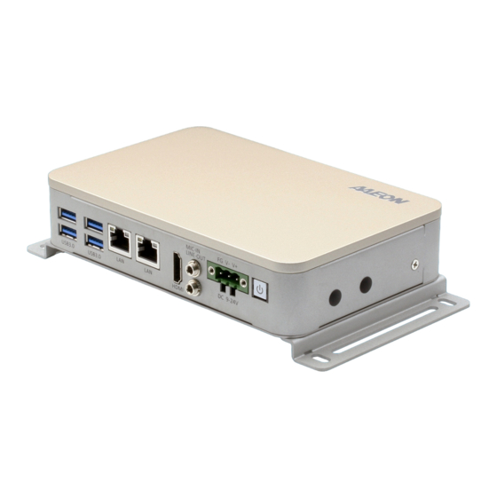
- Page 1 BOXER-8310AI Compact Fanless Embedded AI@Edge Box PC User’s Manual 1 Last Updated: August 14, 2019...
- Page 2 AAEON assumes no liabilities resulting from errors or omissions in this document, or from the use of the information contained herein. AAEON reserves the right to make changes in the product design without notice to its users.
- Page 3 Acknowledgement All other products’ name or trademarks are properties of their respective owners. Microsoft Windows is a registered trademark of Microsoft Corp. Intel, Pentium, and Celeron are registered trademarks of Intel Corporation Movidius, Myriad and Myriad X are registered trademarks of Intel Corporation ...
- Page 4 Before setting up your product, please make sure the following items have been shipped: Item Quantity BOXER-8310AI with built-in Intel Myriad X 3 Pin DC-In Power Connector Wallmount bracket If any of these items are missing or damaged, please contact your distributor or sales representative immediately.
- Page 5 (if any), its specifications, dimensions, jumper/connector settings/definitions, and driver installation instructions (if any), to facilitate users in setting up their product. Users may refer to the product page on AAEON.com for the latest version of this document. Preface...
- Page 6 All cautions and warnings on the device should be noted. All cables and adapters supplied by AAEON are certified and in accordance with the material safety laws and regulations of the country of sale. Do not use any cables or adapters not supplied by AAEON to prevent system malfunction or fires.
- Page 7 As most electronic components are sensitive to static electrical charge, be sure to ground yourself to prevent static charge when installing the internal components. Use a grounding wrist strap and contain all electronic components in any static-shielded containers. If any of the following situations arises, please the contact our service personnel: Damaged power cord or plug Liquid intrusion to the device iii.
- Page 8 FCC Statement This device complies with Part 15 FCC Rules. Operation is subject to the following two conditions: (1) this device may not cause harmful interference, and (2) this device must accept any interference received including interference that may cause undesired operation.
- Page 9 China RoHS Requirements (CN) 产品中有毒有害物质或元素名称及含量 AAEON System QO4-381 Rev.A0 有毒有害物质或元素 部件名称 铅 汞 镉 六价铬 多溴联苯 多溴二苯醚 (Pb) (Hg) (Cd) (Cr(VI)) (PBB) (PBDE) 印刷电路板 × ○ ○ ○ ○ ○ 及其电子组件 外部信号 × ○ ○ ○ ○ ○ 连接器及线材 ○...
- Page 10 China RoHS Requirement (EN) Hazardous and Toxic Materials List AAEON System QO4-381 Rev.A0 Hazardous or Toxic Materials or Elements Component Name PCB and Components Wires & Connectors for Ext. Connections Chassis CPU & RAM HDD Drive LCD Module Optical Drive...
- Page 11 2. Individual components including the CPU, RAM/memory, HDD, optical drive, and PSU are optional. 3. LCD Module and Touch Control Module only applies to certain products which feature these components Preface...
-
Page 12: Table Of Contents
Table of Contents Chapter 1 - Product Specifications ....................1 Specifications ....................... 2 Chapter 2 – Hardware Information ..................... 5 Dimensions ........................6 Jumpers and connectors ................... 7 List of Jumpers ......................8 2.3.1 Setting Jumpers ..................8 2.3.2 Auto Power Button (JP5) ................9 2.3.3 Clear CMOS (JP10) .................. - Page 13 Installing DRAM and mSATA modules ..............22 Chapter 3 - AMI BIOS Setup ...................... 26 System Test and Initialization................. 27 AMI BIOS Setup ......................28 Setup Submenu: Main .................... 29 Setup Submenu: Advanced ................... 30 3.4.1 Advanced: Trusted Computing ............. 31 3.4.2 Advanced: CPU Configuration .............
- Page 14 Appendix B - I/O Information ....................65 I/O Address Map ...................... 66 Memory Address Map .................... 68 IRQ Mapping Chart ....................69 Appendix C – Digital I/O Ports ....................70 Electrical Specifications for Digital I/O Ports ............71 DIO Programming ....................72 Digital I/O Register....................
-
Page 15: Chapter 1 - Product Specifications
Chapter 1 Chapter 1 - Product Specifications... -
Page 16: Specifications
Specifications System Intel® Celeron™ N3350, Pentium™ N4200 Intel® System on Chip Chipset DDR3L SO-DIMM slot x 1 Supports 1867 MHz System Memory and up to 8GB Intel® Movidius™ Myriad™ X x1 AI Solution HDMI 1.4 Display Interface mSATA Storage Device 10/100/1000 Base-TX x2 Ethernet Power Button x 1... - Page 17 System Half-size Minicard slot x 1 (mSATA only) Expansion Power LED x1 Indicator HDD active LED x1 Windows® 10, Windows® 10 IoT OS Support Linux Debian 9.8 Power Supply 3 Pin 9-24V DC-in terminal block Power Requirement Mechanical Wallmount Mounting 6.54"...
- Page 18 Chapter 1 – Product Specifications...
-
Page 19: Chapter 2 - Hardware Information
Chapter 2 Chapter 2 – Hardware Information... -
Page 20: Dimensions
Dimensions BOXER-8310AI Chapter 2 – Hardware Information... -
Page 21: Jumpers And Connectors
Jumpers and connectors Chapter 2 – Hardware Information... -
Page 22: List Of Jumpers
List of Jumpers Please refer to the table below for all of the system’s jumpers that you can configure for your application Label Function AT/ATX mode select JP10 Clear CMOS 2.3.1 Setting Jumpers You configure your card to match the needs of your application by setting jumpers. A jumper is the simplest kind of electric switch. -
Page 23: Auto Power Button (Jp5)
2.3.2 Auto Power Button (JP5) 1 2 3 Disable Enable (Default) Function ATX (Default)- 2.3.3 Clear CMOS (JP10) 1 2 3 JP10 Function Normal (Default) Clear CMOS Chapter 2 – Hardware Information... -
Page 24: List Of Connectors
List of Connectors Please refer to the table below for all of the system’s connectors that you can configure for your application Label Function SATA PWR connector SATA connector Minicard connector Audio Jack Connector (BOX connector) SPI ROM connector COM2 Port BOX connector (RS232/422/485) CN12 COM3 Port BOX connector (RS232/422/485) CN14... - Page 25 Label Function CN54 USB 2.0 Connector (BOX connector) CN61 HDMI connector CN63 Remote button connector CN64 CRT port CN65 CRT port (BOX connector) BAT1 RTC battery connector DIMM1 SO DIMM connector SIM1 SIM1 card connector Power button connector (BOX connector) Chapter 2 –...
-
Page 26: Sata Pwr Port (Cn3)
2.4.1 SATA PWR Port (CN3) Pin Name Level +12V Chapter 2 – Hardware Information... -
Page 27: Sata Port (Cn4)
2.4.2 SATA Port (CN4) Pin 1 Pin 7 Pin Name Signal Type Signal Level GND # SATA_TX+ DIFF SATA_TX- DIFF SATA_RX- DIFF SATA_RX+ DIFF 2.4.3 Mini Card Connector (CN5/CN33) Signal Signal PCIE_WAKE# +V3.3A +1.5V PCIE_CLK_REQ# UIM_PWR UIM_DATA PCIE_REF_CLK- UIM_CLK PCIE_REF_CLK+ UIM_RST UIM_VPP Chapter 2 –... -
Page 28: Spi Rom Connector For Debugging (Cn8)
Signal Signal W_DISABLE# PCIE_RST# PCIE_RX- +V3.3A PCIE_RX+ +1.5V SMB_CLK PCIE_TX- SMB_DATA PCIE_TX+ USB_D- USB_D+ +V3.3A +V3.3A +1.5V +V3.3A 2.4.4 SPI ROM connector for debugging (CN8) Signal Signal SPI_VCC SPI_CE SPI_CLK SPI_DATA_OUT SPI_DATA_IN Chapter 2 – Hardware Information... -
Page 29: Com Port Rs-232/422/485 Box Connector
2.4.5 COM port RS-232/422/485 BOX connector (CN9/CN12/CN14/CN18) RS-232 RS-422 RS-485 DATA- DATA+ Chapter 2 – Hardware Information... -
Page 30: Usb 3.0 (Cn26, Cn27)
2.4.6 USB 3.0 (CN26, CN27) Signal Signal VBUS_1 VBUS_2 (A)D- (B)D- (A)D+ (B)D+ (A)SSRX- (B)SSRX- (A)SSRX+ (B)SSRX+ (A)SSTX- (B)SSTX- (A)SSTX+ (B)SSTX+ Chapter 2 – Hardware Information... -
Page 31: Com Port Rs-232/422/485 (Cn30/Cn31/Cn37)
2.4.7 COM port RS-232/422/485 (CN30/CN31/CN37) RS-232 RS-422 RS-485 DATA- DATA+ 2.4.8 Power Switch connector (internal BOX connector) (CN36) Signal Signal PANSWH# GND- Chapter 2 – Hardware Information... -
Page 32: Dc-In (Cn38)
2.4.9 DC-IN (CN38) Signal Signal PWR_IN 2.4.10 LPC Port (CN45) Pin Name Signal Type Signal Level LAD0 +3.3V LAD1 +3.3V LAD2 +3.3V LAD3 +3.3V +3.3V +3.3V LFRAME# LRESET# +3.3V LCLK I2C CLK +3.3V I2C DATA +3.3V SERIRQ +3.3V Chapter 2 – Hardware Information... -
Page 33: Usb2.0 Connector (Internal Box Connector) (Cn53, Cn54)
2.4.11 USB2.0 connector (internal BOX connector) (CN53, CN54) Signal Signal VBUS USB1- USB+ 2.4.12 HDMI Port (CN61) Signal Signal HDMI_DATA2_P HDMI_DATA2_N HDMI_DATA1_P HDMI_DATA1_N HDMI_DATA0_P HDMI_DATA0_N HDMI_CLK_P HDMI_CLK_N HDMI_SCL HDMI_SDA HDMI_PWR HDMI_HDP Chapter 2 – Hardware Information... -
Page 34: Remote Switch Connector (Cn63)
2.4.13 Remote switch connector (CN63) Signal Signal PANSWH# 2.4.14 VGA Port (CN64) Signal Signal Green Blue VGA_VCC DDC_DATA HSYNC VSYNC DDC_CLK Chapter 2 – Hardware Information... -
Page 35: Vga Port Box Connector (Cn65)
2.4.15 VGA port BOX connector (CN65) Signal Signal VSYNC HSYNC DDC_CLK DDC_DATA Blue Green VGA_VCC Chapter 2 – Hardware Information... -
Page 36: Installing Dram And Msata Modules
Installing DRAM and mSATA modules Remove the screws as shown below; then remove the cover. Chapter 2 – Hardware Information... - Page 37 To install RAM modules, insert the RAM at an angle and push down to secure. Place the thermal pads between the RAM module and RAM Heat Sink as well as between the RAM Heat Sink and chassis as shown below. Secure the assembly per the diagram below.
- Page 38 To install mSATA storage, insert mSATA device into slot at an angle as shown. Push down and secure as in the picture below: Chapter 2 – Hardware Information...
- Page 39 Re-tighten the screws. Chapter 2 – Hardware Information...
-
Page 40: Chapter 3 - Ami Bios Setup
Chapter 3 Chapter 3 - AMI BIOS Setup... -
Page 41: System Test And Initialization
System Test and Initialization The system uses certain routines to perform testing and initialization during the boot up sequence. If an error, fatal or non-fatal, is encountered, the system will output a few short beeps or an error message. The board can usually continue the boot up sequence with non-fatal errors. -
Page 42: Ami Bios Setup
AMI BIOS Setup The AMI BIOS ROM has a pre-installed Setup program that allows users to modify basic system configurations, which is stored in the battery-backed CMOS RAM and BIOS NVRAM so that the information is retained when the power is turned off. To enter BIOS Setup, press <Del>... -
Page 43: Setup Submenu: Main
Setup Submenu: Main Chapter 3 – AMI BIOS Setup... -
Page 44: Setup Submenu: Advanced
Setup Submenu: Advanced Chapter 3 – AMI BIOS Setup... -
Page 45: Advanced: Trusted Computing
3.4.1 Advanced: Trusted Computing Options Summary Security Device Disabled Optimal Default, Failsafe Default Support Enabled Enable/Disable Security Device. NOTE: Your Computer will reboot during restart in order to change State of the Device. SHA-1 PCR Bank Disabled Enabled Optimal Default, Failsafe Default Enable or Disable SHA-1 PCR Bank SHA256 PCR Bank Disabled... - Page 46 Options Summary Platform Hierarchy Disabled Enabled Optimal Default, Failsafe Default Enable or Disable Platform Hierarchy Storage Hierarchy Disabled Enabled Optimal Default, Failsafe Default Enable or Disable Storage Hierarchy Endorsement Disabled Hierarchy Enabled Optimal Default, Failsafe Default Enable or Disable Endorsement Hierarchy TPM2.0 UEFI Spec TCG_2 Optimal Default, Failsafe Default...
-
Page 47: Advanced: Cpu Configuration
3.4.2 Advanced: CPU Configuration Chapter 3 – AMI BIOS Setup... - Page 48 Options Summary Active Processor Disabled Optimal Default, Failsafe Default Cores Enabled Number of cores to enable in each processor package Intel Virtualization Disabled Technology Enabled Optimal Default, Failsafe Default When enabled, a VMM can utilize the additional hardware capabilities provided by Vanderpool Technology.
- Page 49 Options Summary Boot performance Max performance Optimal Default, Failsafe Default mode Max battery Select the performance state that the BIOS will set before OS handoff Power Limit 1 Enable Disabled Optimal Default, Failsafe Default Enabled Enable/Disable Power Limit 1 C-States Disabled Optimal Default, Failsafe Default Enabled...
-
Page 50: Advanced: Sata Drives
3.4.3 Advanced: SATA Drives Options Summary Chipset SATA Enable Optimal Default, Failsafe Default Disable Enable or Disable the Chipset SATA Controller. The Chipset SATA controller supports the 2 black internal SATA ports (up to 3Gb/s supported per port) Port Enable Optimal Default, Failsafe Default Disable Enable or Disable SATA Port... -
Page 51: Advanced: Hardware Monitor
3.4.4 Advanced: Hardware Monitor Chapter 3 – AMI BIOS Setup... -
Page 52: Advanced: Sio Configuration
3.4.5 Advanced: SIO Configuration Chapter 3 – AMI BIOS Setup... -
Page 53: Sio Configuration: Serial Port 1 Configuration
3.4.5.1 SIO Configuration: Serial Port 1 Configuration Options Summary Use This Device Disabled Enabled Optimal Default, Failsafe Default Enable or Disable this Logical Device. Possible: Use Automatic Settings Optimal Default, Failsafe Default IO=3F8; IRQ=4; IO=2F8; IRQ=3; Allows the user to change the device resource settings. New settings will be reflected on this setup page after system restarts. -
Page 54: Sio Configuration: Serial Port 2 Configuration
3.4.5.2 SIO Configuration: Serial Port 2 Configuration Options Summary Use This Device Disabled Enabled Optimal Default, Failsafe Default Enable or Disable this Logical Device. Possible: Use Automatic Settings Optimal Default, Failsafe Default IO=2F8; IRQ=3; IO=3F8; IRQ=4; Allows the user to change the device resource settings. New settings will be reflected on this setup page after system restarts. -
Page 55: Sio Configuration: Serial Port 3 Configuration
3.4.5.3 SIO Configuration: Serial Port 3 Configuration Options Summary Use This Device Disabled Enabled Optimal Default, Failsafe Default Enable or Disable this Logical Device. Possible: Use Automatic Settings Optimal Default, Failsafe Default IO=3E8; IRQ=11; IO=2E8; IRQ=11; Allows the user to change the device resource settings. New settings will be reflected on this setup page after system restarts. -
Page 56: Power Management
3.4.6 Power Management Options Summary Power Mode ATX Type Optimal Default, Failsafe Default AT Type Select system power mode. Restore AC Power Loss Last State Optimal Default, Failsafe Default Power On Power Loss RTC wake system from S5 Disabled Optimal Default, Failsafe Default Fixed Time Dynamic Time Enable or disable System wake on alarm event. -
Page 57: Setup Submenu: Chipset
Setup submenu: Chipset Chapter 3 – AMI BIOS Setup... -
Page 58: Chipset: North Bridge
3.5.1 Chipset: North Bridge Options Summary DCMT Total Gfx 128M Optimal Default, Failsafe Default 256M Select DVMT5.0 Total Graphics Memory size used by the Internal Graphics Device Chapter 3 – AMI BIOS Setup... -
Page 59: Chipset: South Bridge
3.5.2 Chipset: South Bridge Options Summary HD-Audio Support Disable Optimal Default, Failsafe Default Enable Enable/Disable HD-Audio Support Mini-Card 1 Speed Auto Optimal Default, Failsafe Default Gen 1 Gen 2 Configure PCIe Speed Mini-Card 2 Speed Auto Optimal Default, Failsafe Default Gen 1 Gen 2 Configure PCIe Speed... -
Page 60: Setup Submenu: Security
Setup submenu: Security Change User/Administrator Password You can set an Administrator Password or User Password. An Administrator Password must be set before you can set a User Password. The password will be required during boot up, or when the user enters the Setup utility. A User Password does not provide access to many of the features in the Setup utility. -
Page 61: Secure Boot
3.6.1 Secure Boot Options Summary Attempt Secure Disable Optimal Default, Failsafe Default Boot Enable Secure Boot activated when Platform key(PK) is enrolled, System mode is User/Deployed, and CSM function is disabled Enter Audit Mode Enter Audit Mode. If current System Mode is User – PK variable will be erased on transition to Audit. -
Page 62: Key Management
3.6.2 Key Management Options Summary Provision Factory Disable Optimal Default, Failsafe Default Default keys Enable Allow to provision factory default Secure Boot keys when System is in Setup Mode Install Factory Press ‘Yes’ to install factory default Default Keys keys Force System to User Mode –... - Page 63 Enroll Efi Image Settings Enroll Efi Acpi(a0341d0, $AttrDef Image 0)\PCI(12|0)\DevicePath(Type 3, $BadClus SubType 18)HD(Part1, Sig )\ $Bitmap $Boot $LogFile $MFT $MFTMirr $Secure $UpCase $Volume <System Volume Information> <Recovery> <.> <$Extend> Acpi(a0341d0, <EFI> 0)\PCI(12|0)\DevicePath(Type 3, SubType 18)HD(Part2, Sig )\ Chapter 3 – AMI BIOS Setup...
- Page 64 Enroll Efi Image Settings Acpi(a0341d0, $AttrDef 0)\PCI(12|0)\DevicePath(Type 3, $BadClus SubType 18)HD(Part4, Sig )\ $Bitmap $Boot $LogFile $MFT $MFTMirr $Secure $UpCase $Volume bootmgr BOOTNXT hiberfil.sys pagefile.sys swapfile.sys <Windows.old> <Windows> <Users> <System Volume Information> <Recovery> <ProgramData> <Program Files (x86)> <Program Files> <PerfLogs> <Intel>...
- Page 65 Secure Boot Variable Secure Boot Variable Settings Platform key(PK) Set New Var No Press ‘Yes’ to load factory default ‘PK’ or Select ‘No’ to load it from a file on external media Key Exchange keys Set New Var No Press ‘Yes’ to load factory default ‘KEK’ or Select ‘No’...
-
Page 66: Setup Submenu: Boot
Setup submenu: Boot Options Summary Quiet Boot Disabled Enabled Optimal Default, Failsafe Default Enable or Disable Quiet Boot option Network Stack Disabled Optimal Default, Failsafe Default Enabled Enable/Disable UEFI Network Stack Chapter 3 – AMI BIOS Setup... -
Page 67: Setup Submenu: Save & Exit
Setup submenu: Save & Exit Chapter 3 – AMI BIOS Setup... -
Page 68: Chapter 4 - Drivers Installation
Chapter 4 Chapter 4 – Drivers Installation... -
Page 69: Driver Download And Installation
Driver Download and Installation Drivers for the BOXER-8310AI can be downloaded from the product page on the AAEON website by following this link: https://www.aaeon.com/en/p/ai-edge-computing-fanless-box-pc-boxer-8310ai Download the driver(s) you need and follow the steps below to install them. Step 1 – Install Chipset Drivers Open the Step 1 - Chipset folder and select your OS Open the SetupChipset.exe file in the folder... - Page 70 Step 4 – Install USB 3.0 Drivers (Windows 7 only) Open the Step 4 – USB 3.0 followed by the Setup.exe file Follow the instructions Drivers will be installed automatically Step 5 – Install MBI Drivers Open the Step 5 – MBI(Optional) folder and select your OS Open the Setup.exe file Follow the instructions Drivers will be installed automatically...
- Page 71 Open the Step 6 - Serial Port Driver (Optional) folder and run patch.bat as administrator Chapter 4 – Driver Installation...
- Page 72 For Windows 8 and Windows 10: Open the Step 6 - Serial Port Driver (Optional) folder and select your OS Open the batch.bat file in the folder Follow the instructions Drivers will be installed automatically Chapter 4 – Driver Installation...
-
Page 73: Appendix A - Watchdog Timer Programming
Appendix A Appendix A - Watchdog Timer Programming... -
Page 74: Watchdog Timer Initial Program
Watchdog Timer Initial Program Table 1 : SuperIO relative register table Default Value Note SIO MB PnP Mode Index Register Index 0x2E(Note1) 0x2E or 0x4E SIO MB PnP Mode Data Register Data 0x2F(Note2) 0x2F or 0x4F Table 2 : Watchdog relative register table Register BitNum Value... -
Page 75: A.2 Watchdog Sample Program
A.2 Watchdog Sample Program ************************************************************************************ // SuperIO relative definition (Please reference to Table 1) #define byte SIOIndex //This parameter is represented from Note1 #define byte SIOData //This parameter is represented from Note2 #define void IOWriteByte(byte IOPort, byte Value); #define byte IOReadByte(byte IOPort); // Watch Dog relative definition (Please reference to Table 2) #define byte TimerLDN //This parameter is represented from Note3 #define byte TimerReg //This parameter is represented from Note4... - Page 76 ************************************************************************************ VOID Main(){ // Procedure : AaeonWDTConfig // (byte)Timer : Time of WDT timer.(0x00~0xFF) // (boolean)Unit : Select time unit(0: second, 1: minute). AaeonWDTConfig(); // Procedure : AaeonWDTEnable // This procudure will enable the WDT counting. AaeonWDTEnable(); ************************************************************************************ Appendix A – Watchdog Timer Programming...
- Page 77 ************************************************************************************ // Procedure : AaeonWDTEnable VOID AaeonWDTEnable (){ WDTEnableDisable(EnableLDN, EnableReg, EnableBit, 1); // Procedure : AaeonWDTConfig VOID AaeonWDTConfig (){ // Disable WDT counting WDTEnableDisable(EnableLDN, EnableReg, EnableBit, 0); // Clear Watchdog Timeout Status WDTClearTimeoutStatus(); // WDT relative parameter setting WDTParameterSetting(); VOID WDTEnableDisable(byte LDN, byte Register, byte BitNum, byte Value){ SIOBitSet(LDN, Register, BitNum, Value);...
- Page 78 ************************************************************************************ VOID SIOEnterMBPnPMode(){ IOWriteByte(SIOIndex, 0x87); IOWriteByte(SIOIndex, 0x87); VOID SIOExitMBPnPMode(){ IOWriteByte(SIOIndex, 0xAA); VOID SIOSelectLDN(byte LDN){ IOWriteByte(SIOIndex, 0x07); // SIO LDN Register Offset = 0x07 IOWriteByte(SIOData, LDN); VOID SIOBitSet(byte LDN, byte Register, byte BitNum, byte Value){ Byte TmpValue; SIOEnterMBPnPMode(); SIOSelectLDN(byte LDN); IOWriteByte(SIOIndex, Register); TmpValue = IOReadByte(SIOData);...
-
Page 79: Appendix B - I/O Information
Appendix B Appendix B - I/O Information... -
Page 80: I/O Address Map
I/O Address Map Appendix B – I/O Information... - Page 81 Appendix B – I/O Information...
-
Page 82: Memory Address Map
Memory Address Map Appendix B – I/O Information... -
Page 83: Irq Mapping Chart
IRQ Mapping Chart Appendix B – I/O Information... -
Page 84: Appendix C - Digital I/O Ports
Appendix C Appendix C – Digital I/O Ports... -
Page 85: Electrical Specifications For Digital I/O Ports
Electrical Specifications for Digital I/O Ports GPIO50 DIO_0 GPIO51 DIO_1 GPIO52 DIO_2 GPIO53 DIO_3 GPIO54 DIO_4 GPIO55 DIO_5 GPIO56 DIO_6 GPIO57 DIO_7 Appendix C – Digital I/O Ports... -
Page 86: C.2 Dio Programming
C.2 DIO Programming The BOXER-8310AI utilizes FINTEK F81866 chipset as its Digital I/O controller. Below are the procedures to complete its configuration. AAEON initial DI/O program is also attached for developing customized program for your application. There are three steps to complete the configuration setup:... -
Page 87: C.3 Digital I/O Register
C.3 Digital I/O Register Table 1 : SuperIO relative register table Default Value Note SIO MB PnP Mode Index Register Index 0x2E(Note1) 0x2E or 0x4E SIO MB PnP Mode Data Register Data 0x2F(Note2) 0x2F or 0x4F Table 2 : Digital Input relative register table Register BitNum Value... -
Page 88: C.4 Digital I/O Sample Program
C.4 Digital I/O Sample Program ************************************************************************************ // SuperIO relative definition (Please reference to Table 1) #define byte SIOIndex //This parameter is represented from Note1 #define byte SIOData //This parameter is represented from Note2 #define void IOWriteByte(byte IOPort, byte Value); #define byte IOReadByte(byte IOPort); // Digital Input Status relative definition (Please reference to Table 2) #define byte DInput1LDN // This parameter is represented from Note3 #define byte DInput1Reg // This parameter is represented from Note4... - Page 89 ************************************************************************************ // Digital Output control relative definition (Please reference to Table 3) #define byte DOutput1LDN // This parameter is represented from Note27 #define byte DOutput1Reg // This parameter is represented from Note28 #define byte DOutput1Bit // This parameter is represented from Note29 #define byte DOutput1Val // This parameter is represented from Note30 #define byte DOutput2LDN // This parameter is represented from Note31 #define byte DOutput2Reg // This parameter is represented from Note32...
- Page 90 ************************************************************************************ VOID Main(){ Boolean PinStatus ; // Procedure : AaeonReadPinStatus // Input : Example, Read Digital I/O Pin 3 status // Output : InputStatus : 0: Digital I/O Pin level is low 1: Digital I/O Pin level is High PinStatus = AaeonReadPinStatus(DInput3LDN, DInput3Reg, DInput3Bit); // Procedure : AaeonSetOutputLevel // Input : Example, Set Digital I/O Pin 6 level...
- Page 91 ************************************************************************************ Boolean AaeonReadPinStatus(byte LDN, byte Register, byte BitNum){ Boolean PinStatus ; PinStatus = SIOBitRead(LDN, Register, BitNum); Return PinStatus ; VOID AaeonSetOutputLevel(byte LDN, byte Register, byte BitNum, byte Value){ ConfigToOutputMode(LDN, Register, BitNum); SIOBitSet(LDN, Register, BitNum, Value); ************************************************************************************ Appendix C – Digital I/O Ports...
- Page 92 ************************************************************************************ VOID SIOEnterMBPnPMode(){ IOWriteByte(SIOIndex, 0x87); IOWriteByte(SIOIndex, 0x87); VOID SIOExitMBPnPMode(){ IOWriteByte(SIOIndex, 0xAA); VOID SIOSelectLDN(byte LDN){ IOWriteByte(SIOIndex, 0x07); // SIO LDN Register Offset = 0x07 IOWriteByte(SIOData, LDN); VOID SIOBitSet(byte LDN, byte Register, byte BitNum, byte Value){ Byte TmpValue; SIOEnterMBPnPMode(); SIOSelectLDN(byte LDN); IOWriteByte(SIOIndex, Register); TmpValue = IOReadByte(SIOData);...
- Page 93 ************************************************************************************ Boolean SIOBitRead(byte LDN, byte Register, byte BitNum){ Byte TmpValue; SIOEnterMBPnPMode(); SIOSelectLDN(LDN); IOWriteByte(SIOIndex, Register); TmpValue = IOReadByte(SIOData); TmpValue &= (1 << BitNum); SIOExitMBPnPMode(); If(TmpValue == 0) Return 0; Return 1; VOID ConfigToOutputMode(byte LDN, byte Register, byte BitNum){ Byte TmpValue, OutputEnableReg; OutputEnableReg = Register-1;...
- Page 94 Appendix D Appendix D – AI Core X...
-
Page 95: Appendix D - Ai Core X
The User Manual for the AI Core X is included in this document following this section. To view the AI Core X manual by itself, you can download a copy from the product page here: https://www.aaeon.com/en/p/ai-edge-computing-board-ai-core-x Appendix D – AI Core X... - Page 96 AI Core X PER-TAICX-A10-001 Intel Myriad X mPCIe Module User’s Manual 1 Last Updated: May 7, 2019...
- Page 97 AAEON assumes no liabilities resulting from errors or omissions in this document, or from the use of the information contained herein. AAEON reserves the right to make changes in the product design without notice to its users.
- Page 98 Acknowledgements All other products’ name or trademarks are properties of their respective owners. Microsoft Windows® and Windows® 10 are registered trademarks of Microsoft Corp. Ubuntu is a registered trademark of Canonical Intel®, Movidius™, Myriad™, and Myriad™ X are registered trademarks of Intel ...
- Page 99 Packing List Before setting up your product, please make sure the following items have been shipped: Item Quantity AI Core X module card M2 screw If any of these items are missing or damaged, please contact your distributor or sales representative immediately.
- Page 100 (if any), its specifications, dimensions, jumper/connector settings/definitions, and driver installation instructions (if any), to facilitate users in setting up their product. Users may refer to the product page on AAEON.com for the latest version of this document. Preface...
- Page 101 Safety Precautions Please read the following safety instructions carefully. It is advised that you keep this manual for future references All cautions and warnings on the device should be noted. Make sure the power source matches the power rating of the device. Position the power cord so that people cannot step on it.
- Page 102 Do NOT disassemble the motherboard so as not to damage the system or void your warranty. If the thermal pad had been damaged, please contact AAEON's salesperson to purchase a new one. Do NOT use those of other brands. The Hex Cylinder Coppers on the front panel are not removable.
- Page 103 FCC Statement This device complies with Part 15 FCC Rules. Operation is subject to the following two conditions: (1) this device may not cause harmful interference, and (2) this device must accept any interference received including interference that may cause undesired operation. Caution: There is a danger of explosion if the battery is incorrectly replaced.
- Page 104 China RoHS Requirements (CN) 产品中有毒有害物质或元素名称及含量 AAEON Embedded Box PC/ Industrial System 有毒有害物质或元素 部件名称 铅 汞 镉 六价铬 多溴联苯 多溴二苯醚 (Pb) (Hg) (Cd) (Cr(VI)) (PBB) (PBDE) 印刷电路板 ○ ○ ○ ○ ○ ○ 及其电子组件 外部信号 ○ ○ ○ ○ ○ ○...
- Page 105 China RoHS Requirement (EN) Poisonous or Hazardous Substances or Elements in Products AAEON Embedded Box PC/ Industrial System Poisonous or Hazardous Substances or Elements Hexavalent Polybrominated Polybrominated Component Lead Mercury Cadmium Chromium Biphenyls Diphenyl Ethers (Pb) (Hg) (Cd) (Cr(VI)) (PBB) (PBDE) PCB &...
- Page 106 Table of Contents Chapter 1 - Product Specifications ..................1 AI Core X Specifications ..................2 Chapter 2 – Hardware Information ..................3 Dimensions ......................4 Block Diagram ......................5 Board Design ......................6 List of Connectors ....................7 2.4.1 mini-PCIe (CN1) ..................
- Page 107 Chapter 1 Chapter 1 - Product Specifications...
-
Page 108: Ai Core X Specifications
AI Core X Specifications System Intel Movidius Myriad X VPU, MA2485 Tensorflow Supported Frameworks Caffe MXNet Windows 10 Supported OS Ubuntu 16.04 with Intel OpenVINO Others mini-PCIe Form Factor 51 x 30 mm Dimension CE/FCC Class A Certification 0~60°C Operating Temperature 10%~80%RH, non-condensing Operating Humidity Chapter 1 –... -
Page 109: Chapter 2 - Hardware Information
Chapter 2 Chapter 2 – Hardware Information... -
Page 110: Dimensions
Dimensions Chapter 2 – Hardware Information... -
Page 111: Block Diagram
Block Diagram Chapter 2 – Hardware Information... -
Page 112: Board Design
Board Design Bottom Chapter 2 – Hardware Information... -
Page 113: List Of Connectors
List of Connectors This section details the connectors featured on the AI Core X module. This is a reference to help with setup and configuration for your application. Label Function Connector Type mini-PCIe PCIE CONN 52pin (TF)WAFER BOX.2P .180D(M).DIP .1.25mm.PINREX.712-71-02 TW01 (TF)SWITCH.3S.6P .SOJ.24V.25mA.pitch=1.27m SWITCH... - Page 114 Signal Description Signal Description DISABLE# RESET# PCIE_TXN 3.3V PCIE_TXP 1.5V PCIE_RXN PCIE_RXP USB2_DM USB2_DP 3.3V 3.3V 3.3V Chapter 2 – Hardware Information...
-
Page 115: Fan (Cn3)
2.4.2 Fan (CN3) Signal Description Signal Description 2.4.3 Switch (SW1) SW Value Board ID Chapter 2 – Hardware Information... -
Page 116: Chapter 3 - Software Installation
Chapter 3 Chapter 3 – Software Installation... -
Page 117: Intel Openvino Toolkit
Intel OpenVINO Toolkit The AI Core X works with Intel OpenVINO toolkit and does not require any drivers to be installed. Visit the OpenVINO website to download and install the software. https://software.intel.com/en-us/openvino-toolkit Chapter 3 – Driver Installation...
Need help?
Do you have a question about the BOXER-8310AI and is the answer not in the manual?
Questions and answers