
Related Manuals for Aaeon BOXER-6404U


Summary of Contents for Aaeon BOXER-6404U
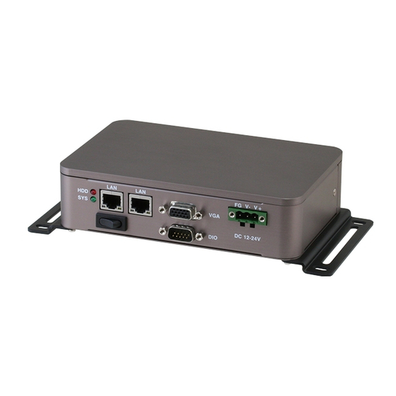
- Page 1 BOXER-6404U Fanless Embedded Box PC User’s Manual 1 Last Updated: December 30, 2016...
- Page 2 AAEON assumes no liabilities resulting from errors or omissions in this document, or from the use of the information contained herein. AAEON reserves the right to make changes in the product design without notice to its users.
- Page 3 Acknowledgement All other products’ name or trademarks are properties of their respective owners. Microsoft Windows is a registered trademark of Microsoft Corp. Intel, Pentium, Celeron, and Xeon are registered trademarks of Intel Corporation Atom is a trademark of Intel Corporation ...
- Page 4 Packing List Before setting up your product, please make sure the following items have been shipped: Item Quantity BOXER-6404U Phoenix power connector Wallmount bracket Product DVD with User’s Manual (in pdf) and drivers If any of these items are missing or damaged, please contact your distributor or sales representative immediately.
- Page 5 (if any), its specifications, dimensions, jumper/connector settings/definitions, and driver installation instructions (if any), to facilitate users in setting up their product. Users may refer to the AAEON.com for the latest version of this document. Preface...
- Page 6 All cautions and warnings on the device should be noted. All cables and adapters supplied by AAEON are certified and in accordance with the material safety laws and regulations of the country of sale. Do not use any cables or adapters not supplied by AAEON to prevent system malfunction or fires.
- Page 7 As most electronic components are sensitive to static electrical charge, be sure to ground yourself to prevent static charge when installing the internal components. Use a grounding wrist strap and contain all electronic components in any static-shielded containers. If any of the following situations arises, please the contact our service personnel: Damaged power cord or plug Liquid intrusion to the device iii.
- Page 8 FCC Statement This device complies with Part 15 FCC Rules. Operation is subject to the following two conditions: (1) this device may not cause harmful interference, and (2) this device must accept any interference received including interference that may cause undesired operation.
- Page 9 China RoHS Requirements (CN) 产品中有毒有害物质或元素名称及含量 AAEON Embedded Box PC/ Industrial System 有毒有害物质或元素 部件名称 铅 汞 镉 六价铬 多溴联苯 多溴二苯醚 (Pb) (Hg) (Cd) (Cr(VI)) (PBB) (PBDE) 印刷电路板 ○ ○ ○ ○ ○ ○ 及其电子组件 外部信号 ○ ○ ○ ○ ○ ○...
- Page 10 China RoHS Requirement (EN) Poisonous or Hazardous Substances or Elements in Products AAEON Embedded Box PC/ Industrial System Poisonous or Hazardous Substances or Elements Hexavalent Polybrominated Polybrominated Component Lead Mercury Cadmium Chromium Biphenyls Diphenyl Ethers (Pb) (Hg) (Cd) (Cr(VI)) (PBB) (PBDE) PCB &...
-
Page 11: Table Of Contents
Table of Contents Chapter 1 - Product Specifications ..................1 Specifications ......................2 Chapter 2 – Hardware Information ..................5 Dimensions ....................... 6 Jumpers and connectors..................7 List of Jumpers ......................8 2.3.1 Clear CMOS Jumper (JP2) .............. 9 2.3.2 Front Panel Connector (JP3) ............ - Page 12 AMI BIOS Setup ..................... 25 Setup Submenu: Main ..................26 Setup Submenu: Advanced ................. 27 3.4.1 Advanced: CPU Configuration ............ 28 3.4.2 Advanced: IDE Configuration (IDE) ..........29 3.4.3 Advanced: USB Configuration ............. 30 3.4.4 Advanced: Hardware Monitor ............. 31 3.4.5 Advanced: Dynamic Digital IO Configuration ......
- Page 13 Electrical Specifications for Digital I/O Ports ............ 66 DIO Programming ....................67 Digital I/O Register ....................68 Digital I/O Sample Program ................69 Preface XIII...
-
Page 14: Chapter 1 - Product Specifications
Chapter 1 Chapter 1 - Product Specifications... -
Page 15: Specifications
Specifications System Intel® Celeron® Processor J1900 (2M Cache, Processor up to 2.42 GHz) Intel® Celeron® Processor N2807 (1M Cache, up to 2.16 GHz) 204-pin DDR3L 1333/1600 MHz SODIMM x 1, System Memory up to 8 GB (J1900) 204-pin DDR3L 1333/1600 MHz SODIMM x 1, up to 4 GB (N2807) Chipset ... - Page 16 LPC wafer x 1 Windows ® OS Support Windows ® Windows ® Windows ® Embedded Standard 8 Windows ® Embedded Standard 7 Linux by Ubantu Mechanical Aluminum heatsink & Steel chassis Construction Wallmount Mounting VSEA mounting kit (Optional) Din-Rail mounting kit (Optional) 166 x 41.5 x 106.6 mm (6.54 x 1.63 x 4.20") Dimension (W x H x D)
- Page 17 Power Supply 3-pin Phoenix DC Input 12~24V, optional DC Input 110/230V AC adapter. ATX mode Chapter 1 – Product Specifications...
-
Page 18: Chapter 2 - Hardware Information
Chapter 2 Chapter 2 – Hardware Information... -
Page 19: Dimensions
Dimensions Chapter 2 – Hardware Information... -
Page 20: Jumpers And Connectors
Jumpers and connectors Chapter 2 – Hardware Information... -
Page 21: List Of Jumpers
List of Jumpers Please refer to the table below for all of the system’s jumpers that you can configure for your application Label Function Clear CMOS Jumper Front Panel Connector Auto Power Button Enable/Disable Selection Chapter 2 – Hardware Information... -
Page 22: Clear Cmos Jumper (Jp2)
2.3.1 Clear CMOS Jumper (JP2) 1 2 3 1 2 3 1 2 3 1 2 3 Normal (Default) Normal (Default) Clear CMOS Clear CMOS 2.3.2 Front Panel Connector (JP3) Pin Name Pin Name Pin 1 PWR_BTN- Pin 2 PWR_BTN+ Pin 3 HDD_LED- Pin 4... -
Page 23: List Of Connectors
List of Connectors Please refer to the table below for all of the system’s connectors that you can configure for your application Label Function Battery connector DDR3L SO-DIMM Slot LAN1 LAN2 Mini-Card Slot (Full-Mini Card) USB 2.0 X1 CN11 LPC Port CN15 Digital IO Port CN19... -
Page 24: Lan 1 (Rj-45) (Cn4)
2.4.1 LAN 1 (RJ-45) (CN4) ACT/LINK SPEED Pin Name Signal Type Signal Level MDI0+ DIFF MDI0- DIFF MDI1+ DIFF MDI2+ DIFF MDI2- DIFF MDI1- DIFF MDI3+ DIFF MDI3- DIFF 2.4.2 LAN 2 (RJ-45) (CN5) ACT/LINK SPEED Pin Name Signal Type Signal Level MDI0+ DIFF... -
Page 25: Mini-Card Slot (Full-Mini Card) (Cn6)
MDI1- DIFF MDI3+ DIFF MDI3- DIFF 2.4.3 Mini-Card Slot (Full-Mini Card) (CN6) Pin Name Signal Type Signal Level PCIE_WAKE# +3.3VSB +3.3V +1.5V +1.5V PCIE_CLK_REQ# UIM_PWR UIM_DATA PCIE_REF_CLK- DIFF UIM_CLK PCIE_REF_CLK+ DIFF UIM_RST UIM_VPP W_DISABLE# +3.3V Chapter 2 – Hardware Information... - Page 26 Pin Name Signal Type Signal Level PCIE_RST# +3.3V PCIE_RX- DIFF +3.3VSB +3.3V PCIE_RX+ DIFF +1.5V +1.5V SMB_CLK +3.3V PCIE_TX- DIFF SMB_DATA +3.3V PCIE_TX+ DIFF USB_D- DIFF USB_D+ DIFF +3.3VSB +3.3V +3.3VSB +3.3V Chapter 2 – Hardware Information...
-
Page 27: Usb 2.0 Port 1 (Cn9)
Pin Name Signal Type Signal Level +1.5V +1.5V +3.3VSB +3.3V 2.4.4 USB 2.0 Port 1 (CN9) Pin Name Signal Type Signal Level +5VSB USB_D- DIFF USB_D+ DIFF 2.4.5 LPC Port (CN11) LAD0 LAD1 LAD2 LAD3 +3.3V LFRAME# LRESET# LCLK LDRQ0 LDRQ1 SERIRQ Chapter 2 –... -
Page 28: Digital Io Port (Cn15)
Pin Name Signal Type Signal Level LAD0 +3.3V LAD1 +3.3V LAD2 +3.3V LAD3 +3.3V +3.3V +3.3V LFRAME# LRESET# +3.3V LCLK LDRQ0 LDRQ1 SERIRQ +3.3V 2.4.6 Digital IO Port (CN15) DIO0 DIO1 DIO2 DIO3 DIO4 DIO5 DIO6 DIO7 Pin Name Signal Type Signal Level DIO0 DIO1... -
Page 29: Output For Sata Hdd (Cn19)
Pin Name Signal Type Signal Level 2.4.7 +5 V Output for SATA HDD (CN19) Pin Name Signal Type Signal Level +V5S 2.4.8 SATA Port (CN20) Pin 1 Pin 7 Pin Name Signal Type Signal Level SATA_TXP1 DIFF SATA_TXN1 DIFF SATA_RXN1 DIFF SATA_RXP1 DIFF... -
Page 30: External Power Input (Cn39)
2.4.9 External Power Input (CN39) Pin Name Signal Type Signal Level +12V~+24V GND_EARTH 2.4.10 Mini-Card Slot (Half-Mini Card) (CN40) Pin Name Signal Type Signal Level PCIE_WAKE# +3.3VSB +3.3V +1.5V +1.5V PCIE_REF_CLK- DIFF PCIE_REF_CLK+ DIFF Chapter 2 – Hardware Information... - Page 31 Pin Name Signal Type Signal Level W_DISABLE# +3.3V PCIE_RST# +3.3V PCIE_RX- DIFF +3.3VSB +3.3V PCIE_RX+ DIFF +1.5V +1.5V SMB_CLK +3.3V PCIE_TX- DIFF SMB_DATA +3.3V PCIE_TX+ DIFF USB_D- DIFF USB_D+ DIFF +3.3VSB +3.3V Chapter 2 – Hardware Information...
-
Page 32: Uim Card Socket (Push-Push Type) (Cn41)
Pin Name Signal Type Signal Level +3.3VSB +3.3V +1.5V +1.5V +3.3VSB +3.3V 2.4.11 UIM Card Socket (Push-Push type) (CN41) Pin Name Signal Type Signal Level UIM_PWR UIM_RST UIM_CLK UIM_VPP UIM_DATA Chapter 2 – Hardware Information... -
Page 33: Usb3.0 X 1 (Cn42)
2.4.12 USB3.0 x 1 (CN42) Pin Name Signal Type Signal Level USB_D- DIFF USB_D+ DIFF USB3.0 RX- DIFF USB3.0 RX+ DIFF USB3.0 TX- DIFF USB3.0 TX+ DIFF 2.4.13 COM1 (CN43) Pin Name Signal Type Signal Level Chapter 2 – Hardware Information... -
Page 34: Installing Dram
Installing DRAM Remove the screws as shown below; then remove the cover. Chapter 2 – Hardware Information... - Page 35 Put the thermal pad on between the chassis and the RAM, slot in the RAM diagonally into the slot and push down to secure. Re-tighten the screws Chapter 2 – Hardware Information...
-
Page 36: Chapter 3 - Ami Bios Setup
Chapter 3 Chapter 3 - AMI BIOS Setup... -
Page 37: System Test And Initialization
System Test and Initialization The system uses certain routines to perform testing and initialization. If an error, fatal or non-fatal, is encountered, a few short beeps or an error message will be outputted. The board can usually continue the boot up sequence with non-fatal errors. The system configuration verification routines check the current system configuration against the values stored in the CMOS memory. -
Page 38: Ami Bios Setup
AMI BIOS Setup The AMI BIOS ROM has a pre-installed Setup program that allows users to modify basic system configurations, which is stored in the battery-backed CMOS RAM and BIOS NVRAM so that the information is retained when the power is turned off. To enter BIOS Setup, press <Del>... -
Page 39: Setup Submenu: Main
Setup Submenu: Main Chapter 3 – AMI BIOS Setup... -
Page 40: Setup Submenu: Advanced
Setup Submenu: Advanced Chapter 3 – AMI BIOS Setup... -
Page 41: Advanced: Cpu Configuration
3.4.1 Advanced: CPU Configuration Options summary: Intel Virtualization Disabled Technology Enabled Optimal Default, Failsafe Default When enabled, a VMM can utilize the additional hardware capabilities provided by Vanderpool Technology. EIST Disabled Enabled Optimal Default, Failsafe Default Enable/Disable Intel SpeedStep Chapter 3 – AMI BIOS Setup... -
Page 42: Advanced: Ide Configuration (Ide)
3.4.2 Advanced: IDE Configuration (IDE) Options summary: SATA Mode IDE Mode AHCI Mode Optimal Default, Failsafe Default Select IDE / AHCI Chapter 3 – AMI BIOS Setup... -
Page 43: Advanced: Usb Configuration
3.4.3 Advanced: USB Configuration Options summary: Legacy USB Support Enabled Optimal Default, Failsafe Default Disabled Auto Enables BIOS Support for Legacy USB Support. When enabled, USB can be functional in legacy environment like DOS. AUTO option disables legacy support if no USB devices are connected Chapter 3 –... -
Page 44: Advanced: Hardware Monitor
3.4.4 Advanced: Hardware Monitor Chapter 3 – AMI BIOS Setup... -
Page 45: Advanced: Dynamic Digital Io Configuration
3.4.5 Advanced: Dynamic Digital IO Configuration Options summary: GPI[3:0] Direction Input Optimal Default, Failsafe Default Output Set GPIO as Input or Output GPI[3:0] Output Level Optimal Default, Failsafe Default Set GPI[3:0] Output as Hi or Low GPO[3:0] Direction Input Output Optimal Default, Failsafe Default Set GPIO as Input or Output GPO[3:0] Output Level... -
Page 46: Power Management
3.4.6 Power Management Options summary: Power Mode ATX Type Optimal Default, Failsafe Default AT Type Select power supply mode. Restore AC Power Loss Last State Optimal Default, Failsafe Default Power On Power Loss Select power state when power is re-applied after a power failure. Wake on Ring Disabled Optimal Default, Failsafe Default... -
Page 47: Advanced: Sio Configuration
3.4.7 Advanced: SIO Configuration Chapter 3 – AMI BIOS Setup... -
Page 48: Sio Configuration: Serial Port 1 Configuration
3.4.7.1 SIO Configuration: Serial Port 1 Configuration Options summary: Use This Device Disabled Enabled Optimal Default, Failsafe Default En/Disable Serial Port (COM) Possible: Use Automatic Settings Optimal Default, Failsafe Default IO=3F8; IRQ=4; IO=2F8; IRQ=3; Select an optimal setting for IO device Chapter 3 –... -
Page 49: Setup Submenu: Chipset
Setup submenu: Chipset Chapter 3 – AMI BIOS Setup... -
Page 50: Chipset: North Bridge
3.5.1 Chipset: North Bridge Chapter 3 – AMI BIOS Setup... -
Page 51: North Bridge: Display Control Configuration
3.5.1.1 North Bridge: Display Control Configuration Options summary: DVMT Pre-Allocated Optimal Default, Failsafe Default 128M 160M … 512M Select DVMT 5.0 Pre-Allocated (Fixed) Graphics Memory size used by the Internal Graphics Device. DVMT Total Gfx Mem 128MB 256MB Optimal Default, Failsafe Default Select DVMT 5.0 Total Graphics Memory size used by the Internal Graphics Device. -
Page 52: Chipset: South Bridge
3.5.2 Chipset: South Bridge Options summary: Mini-Card 2 Speed Auto Optimal Default, Failsafe Default (CN6) Gen 2 Gen 1 Configure PCIe Port Speed Chapter 3 – AMI BIOS Setup... -
Page 53: Setup Submenu: Security
Setup submenu: Security Change User/Administrator Password You can set a User Password once an Administrator Password is set. The password will be required during boot up, or when the user enters the Setup utility. Please Note that a User Password does not provide access to many of the features in the Setup utility. Select the password you wish to set, press Enter to open a dialog box to enter your password (you can enter no more than six letters or numbers). -
Page 54: Setup Submenu: Boot
Setup submenu: Boot Options summary: Quiet Boot Disabled Enabled Default En/Disable showing boot logo. Option ROM Messages Force BIOS Default Keep Current Set display mode for Option ROM Launch PXE OpROM Disabled Default Enabled Controls the execution of LAN PXE OpROM Chapter 3 –... -
Page 55: Setup Submenu: Save & Exit
Setup submenu: Save & Exit Chapter 3 – AMI BIOS Setup... -
Page 56: Chapter 4 - Drivers Installation
Chapter 4 Chapter 4 – Drivers Installation... -
Page 57: Product Cd/Dvd
Product CD/DVD The BOXER-6404U comes with a product DVD that contains all the drivers and utilities you need to setup your product. Insert the DVD and follow the steps in the autorun program to install the drivers. In case the program does not start, follow the sequence below to install the drivers. - Page 58 Step 4 – Install USB 3.0 Drivers (Windows 7 only) Open the Step 4 – USB 3.0 followed by the Setup.exe file Follow the instructions Drivers will be installed automatically Step 5 – Install MBI Drivers Open the Step 5 – MBI(Optional) folder and select your OS Open the Setup.exe file Follow the instructions Drivers will be installed automatically...
- Page 59 Open the Step 6 - Serial Port Driver (Optional) folder and run patch.bat as administrator Chapter 4 – Driver Installation...
- Page 60 For Windows 8 and Windows 10: Open the Step 6 - Serial Port Driver (Optional) folder and select your OS Open the batch.bat file in the folder Follow the instructions Drivers will be installed automatically Chapter 4 – Driver Installation...
-
Page 61: Appendix A - Watchdog Timer Programming
Appendix A Appendix A - Watchdog Timer Programming... -
Page 62: Watchdog Timer Initial Program
A.1 Watchdog Timer Initial Program Table 1 : SuperIO relative register table Default Value Note SIO MB PnP Mode Index Register Index 0x2E(Note1) 0x2E or 0x4E SIO MB PnP Mode Data Register Data 0x2F(Note2) 0x2F or 0x4F Table 2 : Watchdog relative register table Register BitNum Value... -
Page 63: Watchdog Sample Program
A.2 Watchdog Sample Program ************************************************************************************ // SuperIO relative definition (Please reference to Table 1) #define byte SIOIndex //This parameter is represented from Note1 #define byte SIOData //This parameter is represented from Note2 #define void IOWriteByte(byte IOPort, byte Value); #define byte IOReadByte(byte IOPort); // Watch Dog relative definition (Please reference to Table 2) #define byte TimerLDN //This parameter is represented from Note3 #define byte TimerReg //This parameter is represented from Note4... - Page 64 ************************************************************************************ VOID Main(){ // Procedure : AaeonWDTConfig // (byte)Timer : Time of WDT timer.(0x00~0xFF) // (boolean)Unit : Select time unit(0: second, 1: minute). AaeonWDTConfig(); // Procedure : AaeonWDTEnable // This procudure will enable the WDT counting. AaeonWDTEnable(); ************************************************************************************ Appendix A – Watchdog Timer Programming...
- Page 65 ************************************************************************************ // Procedure : AaeonWDTEnable VOID AaeonWDTEnable (){ WDTEnableDisable(EnableLDN, EnableReg, EnableBit, 1); // Procedure : AaeonWDTConfig VOID AaeonWDTConfig (){ // Disable WDT counting WDTEnableDisable(EnableLDN, EnableReg, EnableBit, 0); // Clear Watchdog Timeout Status WDTClearTimeoutStatus(); // WDT relative parameter setting WDTParameterSetting(); VOID WDTEnableDisable(byte LDN, byte Register, byte BitNum, byte Value){ SIOBitSet(LDN, Register, BitNum, Value);...
- Page 66 ************************************************************************************ VOID SIOEnterMBPnPMode(){ IOWriteByte(SIOIndex, 0x87); IOWriteByte(SIOIndex, 0x87); VOID SIOExitMBPnPMode(){ IOWriteByte(SIOIndex, 0xAA); VOID SIOSelectLDN(byte LDN){ IOWriteByte(SIOIndex, 0x07); // SIO LDN Register Offset = 0x07 IOWriteByte(SIOData, LDN); VOID SIOBitSet(byte LDN, byte Register, byte BitNum, byte Value){ Byte TmpValue; SIOEnterMBPnPMode(); SIOSelectLDN(byte LDN); IOWriteByte(SIOIndex, Register); TmpValue = IOReadByte(SIOData);...
-
Page 67: Appendix B - I/O Information
Appendix B Appendix B - I/O Information... -
Page 68: I/O Address Map
I/O Address Map Appendix B – I/O Information... -
Page 69: Memory Address Map
Memory Address Map Appendix B – I/O Information... -
Page 70: Irq Mapping Chart
IRQ Mapping Chart Appendix B – I/O Information... - Page 71 Appendix B – I/O Information...
- Page 72 Appendix B – I/O Information...
- Page 73 Appendix B – I/O Information...
- Page 74 Appendix B – I/O Information...
- Page 75 Appendix B – I/O Information...
- Page 76 Appendix B – I/O Information...
- Page 77 Appendix B – I/O Information...
-
Page 78: Appendix C - Digital I/O Ports
Appendix C Appendix C – Digital I/O Ports... -
Page 79: Electrical Specifications For Digital I/O Ports
Electrical Specifications for Digital I/O Ports GPIO20 DIO_0 GPIO21 DIO_1 GPIO22 DIO_2 GPIO23 DIO_3 GPIO31 DIO_4 GPIO32 DIO_5 GPIO33 DIO_6 GPIO35 DIO_7 Appendix C – Electrical Specifications for I/O Ports... -
Page 80: Dio Programming
DIO Programming The BOXER-6404U utilizes FINTEK F81801 chipset as its Digital I/O controller. Below are the procedures to complete its configuration. AAEON initial DI/O program is also attached for developing customized program for your application. There are three steps to complete the configuration setup:... -
Page 81: Digital I/O Register
Digital I/O Register Table 1 : SuperIO relative register table Default Value Note SIO MB PnP Mode Index Register Index 0x2E(Note1) 0x2E or 0x4E SIO MB PnP Mode Data Register Data 0x2F(Note2) 0x2F or 0x4F Table 2 : Digital Input relative register table Register BitNum Value... -
Page 82: Digital I/O Sample Program
Digital I/O Sample Program ************************************************************************************ // SuperIO relative definition (Please reference to Table 1) #define byte SIOIndex //This parameter is represented from Note1 #define byte SIOData //This parameter is represented from Note2 #define void IOWriteByte(byte IOPort, byte Value); #define byte IOReadByte(byte IOPort); // Digital Input Status relative definition (Please reference to Table 2) #define byte DInput1LDN // This parameter is represented from Note3 #define byte DInput1Reg // This parameter is represented from Note4... - Page 83 ************************************************************************************ // Digital Output control relative definition (Please reference to Table 3) #define byte DOutput1LDN // This parameter is represented from Note27 #define byte DOutput1Reg // This parameter is represented from Note28 #define byte DOutput1Bit // This parameter is represented from Note29 #define byte DOutput1Val // This parameter is represented from Note30 #define byte DOutput2LDN // This parameter is represented from Note31 #define byte DOutput2Reg // This parameter is represented from Note32...
- Page 84 ************************************************************************************ VOID Main(){ Boolean PinStatus ; // Procedure : AaeonReadPinStatus // Input : Example, Read Digital I/O Pin 3 status // Output : InputStatus : 0: Digital I/O Pin level is low 1: Digital I/O Pin level is High PinStatus = AaeonReadPinStatus(DInput3LDN, DInput3Reg, DInput3Bit); // Procedure : AaeonSetOutputLevel // Input : Example, Set Digital I/O Pin 6 level...
- Page 85 ************************************************************************************ Boolean AaeonReadPinStatus(byte LDN, byte Register, byte BitNum){ Boolean PinStatus ; PinStatus = SIOBitRead(LDN, Register, BitNum); Return PinStatus ; VOID AaeonSetOutputLevel(byte LDN, byte Register, byte BitNum, byte Value){ ConfigToOutputMode(LDN, Register, BitNum); SIOBitSet(LDN, Register, BitNum, Value); ************************************************************************************ Appendix C – Electrical Specifications for I/O Ports...
- Page 86 ************************************************************************************ VOID SIOEnterMBPnPMode(){ IOWriteByte(SIOIndex, 0x87); IOWriteByte(SIOIndex, 0x87); VOID SIOExitMBPnPMode(){ IOWriteByte(SIOIndex, 0xAA); VOID SIOSelectLDN(byte LDN){ IOWriteByte(SIOIndex, 0x07); // SIO LDN Register Offset = 0x07 IOWriteByte(SIOData, LDN); VOID SIOBitSet(byte LDN, byte Register, byte BitNum, byte Value){ Byte TmpValue; SIOEnterMBPnPMode(); SIOSelectLDN(byte LDN); IOWriteByte(SIOIndex, Register); TmpValue = IOReadByte(SIOData);...
- Page 87 ************************************************************************************ Boolean SIOBitRead(byte LDN, byte Register, byte BitNum){ Byte TmpValue; SIOEnterMBPnPMode(); SIOSelectLDN(LDN); IOWriteByte(SIOIndex, Register); TmpValue = IOReadByte(SIOData); TmpValue &= (1 << BitNum); SIOExitMBPnPMode(); If(TmpValue == 0) Return 0; Return 1; VOID ConfigToOutputMode(byte LDN, byte Register, byte BitNum){ Byte TmpValue, OutputEnableReg; OutputEnableReg = Register-1;...
Need help?
Do you have a question about the BOXER-6404U and is the answer not in the manual?
Questions and answers