
Related Manuals for Aaeon BOXER-6842M


Summary of Contents for Aaeon BOXER-6842M
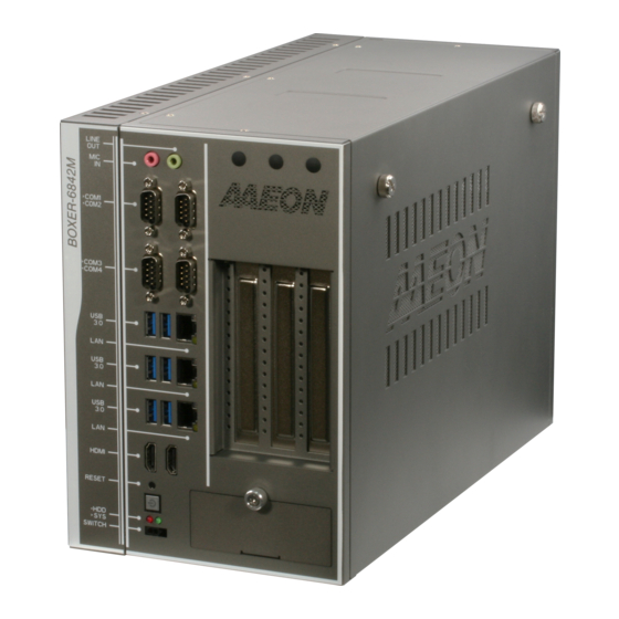
- Page 1 BOXER-6842M Fanless Embedded Box PC User’s Manual 1 Last Updated: May 28, 2020...
- Page 2 AAEON assumes no liabilities resulting from errors or omissions in this document, or from the use of the information contained herein. AAEON reserves the right to make changes in the product design without notice to its users.
- Page 3 Acknowledgements All other products’ name or trademarks are properties of their respective owners. Microsoft Windows ® is a registered trademark of Microsoft Corp. ⚫ Intel , Pentium , Celeron , and Xeon are registered trademarks of Intel ® ® ® ®...
- Page 4 Packing List Before setting up your product, please make sure the following items have been shipped: Item Quantity BOXER-6842M If any of these items are missing or damaged, please contact your distributor or sales representative immediately. Preface...
- Page 5 (if any), its specifications, dimensions, jumper/connector settings/definitions, and driver installation instructions (if any), to facilitate users in setting up their product. Users may refer to the product page on AAEON.com for the latest version of this document. Preface...
- Page 6 Safety Precautions Please read the following safety instructions carefully. It is advised that you keep this manual for future references All cautions and warnings on the device should be noted. Make sure the power source matches the power rating of the device. Position the power cord so that people cannot step on it.
- Page 7 Do NOT disassemble the motherboard so as not to damage the system or void your warranty. If the thermal pad had been damaged, please contact AAEON's salesperson to purchase a new one. Do NOT use those of other brands. The Hex Cylinder Coppers on the front panel are not removable.
- Page 8 FCC Statement This device complies with Part 15 FCC Rules. Operation is subject to the following two conditions: (1) this device may not cause harmful interference, and (2) this device must accept any interference received including interference that may cause undesired operation. Caution: There is a danger of explosion if the battery is incorrectly replaced.
- Page 9 China RoHS Requirements (CN) 产品中有毒有害物质或元素名称及含量 AAEON System QO4-381 Rev.A0 有毒有害物质或元素 部件名称 铅 汞 镉 六价铬 多溴联苯 多溴二苯醚 (Pb) (Hg) (Cd) (Cr(VI)) (PBB) (PBDE) 印刷电路板 × ○ ○ ○ ○ ○ 及其电子组件 外部信号 × ○ ○ ○ ○ ○ 连接器及线材 外壳...
- Page 10 China RoHS Requirement (EN) Hazardous and Toxic Materials List AAEON System QO4-381 Rev.A0 Hazardous or Toxic Materials or Elements Component Name PCB and Components Wires & Connectors for Ext. Connections Chassis CPU & RAM HDD Drive LCD Module Optical Drive...
-
Page 11: Table Of Contents
Table of Contents Chapter 1 - Product Specifications ..................1 Specifications ......................2 Chapter 2 – Hardware Information ..................5 Dimensions ......................6 Jumpers and Connectors ..................10 List of Jumpers ......................11 2.3.1 PCIe [x16] Bifurcation Selection (JP1, JP2) ..........11 2.3.2 Clear CMOS Jumper (JP3) ................. - Page 12 2.4.14 SATA Power Connector (CN21, CN22, CN25, CN27)......31 2.4.15 Digital IO Port (CN28) ................32 2.4.16 COM1, COM2 Connector (RS232/RS422/RS485) (CN29) ....33 2.4.17 COM Port 1 Wafer Box (Optional) (CN30) ..........34 2.4.18 COM Port 2 Wafer Box (Optional) (CN31) ..........35 2.4.19 COM3, COM4 Connector (RS232/RS422/RS485) (CN32) ....
- Page 13 3.4.3 Advanced: PCH-FW Configuration ............68 3.4.3.1 Firmware Update Configuration ............. 69 3.4.3.2 PTT Configuration ................70 3.4.4 Advanced: SATA Configuration ..............71 3.4.5 Advanced: USB Configuration ..............72 3.4.6 Advanced: Hardware Monitor ..............73 3.4.6.1 Smart Fan Mode Configuration ............74 3.4.7 Advanced: SIO Configuration ..............
- Page 14 Appendix A - I/O Information .................... 103 I/O Address Map ....................104 Memory Address Map ..................106 IRQ Mapping Chart .................... 107 Preface...
-
Page 15: Chapter 1 - Product Specifications
Chapter 1 Chapter 1 - Product Specifications... -
Page 16: Specifications
Specifications System Intel® Xeon® E-2124G Intel® i9-9900T Intel® i7-8700T Intel® i5-8500T Intel® i3-8100T Intel® Pentium® G5400T Intel® Celeron® G4900T PS. Support max TPD 71W processor Chipset C246, No H310 downward support System Memory DDR4 SO-DIMM socket x4 (double deck) 2133/2666 MHz up to 128GB Supports un-buffered and ECC/ non-ECC type SODIMM... - Page 17 System Expansion Full-size Mini-card x 1 (PCIE + USB with 1 SIM Slot) Half-size Mini-card x 1 (PCIE + USB, optional for mSATA) M.2 M key (2280) x 1 (PCIE x 4) PCIE [x4] x 1 PCIE [x16] x 1 Max.
- Page 18 Environmental Operating Temperature -4°F ~ 149°F (-20°C ~ 65°C) with 0.5m/s airflow Storage Temperature -49°F ~ 176°F (-45°C ~ 80°C) Storage Humidity 5 ~ 95% @ 40°C, non-condensing Anti-Vibration SSD/mSATA: Random, 3Grm, 5~500Hz HDD: Random, 1Grm, 5~500Hz Certification CE / FCC class A Chapter 1 –...
-
Page 19: Chapter 2 - Hardware Information
Chapter 2 Chapter 2 – Hardware Information... -
Page 20: Dimensions
Dimensions System Chapter 2 – Hardware Information... - Page 21 Chapter 2 – Hardware Information...
- Page 22 Chapter 2 – Hardware Information...
- Page 23 Board Chapter 2 – Hardware Information...
-
Page 24: Jumpers And Connectors
Jumpers and Connectors Chapter 2 – Hardware Information... -
Page 25: List Of Jumpers
List of Jumpers Please refer to the table below for all of the system’s jumpers that you can configure for your application. Label Function PCIe [x16] Bifurcation selection PCIe [x16] Bifurcation selection CMOS Control Selection PCIe and SATA bus selection for M.2 slot PCIe and SATA bus selection for Mini-Card slot JP11 PCIe [x16] lane normal/reversed selection... -
Page 26: Clear Cmos Jumper (Jp3)
2.3.2 Clear CMOS Jumper (JP3) Normal (Default) Clear CMOS 2.3.3 PCIe, SATA Selection for M.2 Slot (JP4) SATA Bus PCIe Bus (Default) 2.3.4 PCIe, SATA Selection for Mini-Card Slot (JP5) 1 2 3 SATA Bus PCIe Bus (Default) 2.3.5 PCIe [x16] Lanes Normal/Reversed (JP11) 1 2 3 Lane Numbers Normal Lane Numbers Reversed (Default) -
Page 27: List Of Connectors
List of Connectors Please refer to the table below for all of the system’s connectors that you can configure for your application Label Function SO-DIMM Channel A0 SO-DIMM Channel A1 SO-DIMM Channel B0 SO-DIMM Channel B1 PCIe [x4] slot PCIe [x16] slot VGA box connector Dual HDMI port LAN (RJ-45) + Dual USB 3.0 Connector... - Page 28 Label Function CN27 SATA PWR connector CN28 DIO box connector CN29 COM1+COM2 Connector RS232/RS422/RS485 CN30 COM1 HEADER RS232/RS422/RS485 CN31 COM2 HEADER RS232/RS422/RS485 CN32 COM3+COM4 Connector RS232/RS422/RS485 CN33 COM3 HEADER RS232/RS422/RS485 CN34 COM4 HEADER RS232/RS422/RS485 CN35 COM5 HEADER RS232/RS422/RS485 CN36 COM6 HEADER RS232/RS422/RS485 CN37 Mini-PCIe slot (Full Size) CN38...
-
Page 29: Pcie [X4] Slot (Cn5)
2.4.1 PCIe [x4] Slot (CN5) Pin name Signal Type Signal Level PRSNT1# +V12S +12V +12V +V12S PCIE_TXN5 DIFF PCIE_TXP5 DIFF PCIE_RXN5 DIFF PCIE_RXP5 DIFF +V3.3S +3.3V +V3.3S +3.3V PERST# PCIE_x4SLOT_CLK DIFF PCIE_x4SLOT_CLK# DIFF PCIE_RXP24 DIFF PCIE_RXN24 DIFF Chapter 2 – Hardware Information... - Page 30 Pin name Signal Type Signal Level PCIE_RXP23 DIFF PCIE_RXN23 DIFF PCIE_RXP22 DIFF PCIE_RXP22 DIFF PCIE_RXP21 DIFF PCIE_RXN21 DIFF +V12S +12V +V12S +12V +V12S +12V SMB_CLK SMB_DATA +V3.3S +V3.3S 3.3Vaux +V3.3A WAKE# PCIE_TXP24 DIFF Chapter 2 – Hardware Information...
- Page 31 Pin name Signal Type Signal Level PCIE_TXN24 DIFF PRSNT PCIE_TXP23 DIFF PCIE_TXN23 DIFF PCIE_TXP22 DIFF PCIE_TXN22 DIFF PCIE_TXP21 DIFF PCIE_TXN21 DIFF PRSNT Chapter 2 – Hardware Information...
-
Page 32: Audio I/O Port (10P Pitch: 1.25Mm) (Cn7)
2.4.2 Audio I/O Port (10P Pitch: 1.25mm) (CN7) Pin name Signal Type Signal Level MIC_L MIC_R GND_AUDIO LINE_L_IN LINE_R_IN GND_AUDIO LEFT_OUT GND_AUDIO RIGHT_OUT +5V_AUDIO 2.4.3 Dual HDMI Port (CN8) Standard Specification Chapter 2 – Hardware Information... -
Page 33: Lan (Rj-45) + Dual Usb 3.0 (Cn9)
2.4.4 LAN (RJ-45) + Dual USB 3.0 (CN9) Note: Dual USB 3.0 ports are USB 3.2 Gen 2 (10 Gbps) specification. LAN (RJ-45) Pin name Signal Type Signal Level DIFF MDI0+ DIFF MDI0- DIFF MDI1+ DIFF MDI2+ DIFF MDI2- DIFF MDI1- DIFF MDI3+... - Page 34 Dual USB 3.0 (USB 3.2 Gen 2) Pin name Signal Type Signal Level +5VSB DIFF USB1_D- DIFF USB1_D+ USB1_SSRX− DIFF USB1_SSRX+ DIFF USB1_SSTX− DIFF USB1_SSTX+ DIFF +5VSB DIFF USB2_D- DIFF USB2_D+ USB2_SSRX− DIFF USB2_SSRX+ DIFF USB2_SSTX− DIFF USB2_SSTX+ DIFF Chapter 2 – Hardware Information...
-
Page 35: Lan (Rj-45) + Dual Usb 3.0 (Cn10)
2.4.5 LAN (RJ-45) + Dual USB 3.0 (CN10) Note: Dual USB 3.0 ports are USB 3.2 Gen 2 (10 Gbps) specification. LAN (RJ-45) Pin name Signal Type Signal Level DIFF MDI0+ DIFF MDI0- DIFF MDI1+ DIFF MDI2+ DIFF MDI2- DIFF MDI1- DIFF MDI3+... - Page 36 Dual USB 3.0 (USB 3.2 Gen 2) Pin name Signal Type Signal Level +5VSB DIFF USB3_D- DIFF USB3_D+ USB3_SSRX− DIFF USB3_SSRX+ DIFF USB3_SSTX− DIFF USB3_SSTX+ DIFF +5VSB DIFF USB4_D- DIFF USB4_D+ USB4_SSRX− DIFF USB4_SSRX+ DIFF USB4_SSTX− DIFF USB4_SSTX+ DIFF Chapter 2 – Hardware Information...
-
Page 37: Lan (Rj-45) + Dual Usb 3.0 (Cn11)
2.4.6 LAN (RJ-45) + Dual USB 3.0 (CN11) Note: Dual USB 3.0 ports are USB 3.2 Gen 2 (10 Gbps) specification. LAN (RJ-45) Pin name Signal Type Signal Level DIFF MDI0+ DIFF MDI0- DIFF MDI1+ DIFF MDI2+ DIFF MDI2- DIFF MDI1- DIFF MDI3+... - Page 38 Dual USB 3.0 (USB 3.2 Gen 2) Pin name Signal Type Signal Level +5VSB DIFF USB5_D- DIFF USB5_D+ USB5_SSRX− DIFF USB5_SSRX+ DIFF USB5_SSTX− DIFF USB5_SSTX+ DIFF +5VSB DIFF USB6_D- DIFF USB6_D+ USB6_SSRX− DIFF USB6_SSRX+ DIFF USB6_SSTX− DIFF USB6_SSTX+ DIFF Chapter 2 – Hardware Information...
-
Page 39: Cpu Fan Connector (Cn12)
2.4.7 CPU FAN Connector (CN12) Pin name Signal Type Signal Level +VCC_FAN_CPU_CON FAN_TAC_CPU_CON FAN_CTL_CPU_CON 2.4.8 System FAN Connector (CN13) Pin name Signal Type Signal Level +VCC_FAN_CPU_CON FAN_TAC_SYS_CON FAN_CTL_SYS_CON Chapter 2 – Hardware Information... -
Page 40: Connector (Cn14)
2.4.9 M.2 Connector (CN14) Pin name Signal Type Signal Level Top (Odd) PCIE_RXN16 PCIE_RXP16 PCIE_TXN16 PCIE_TXP16 PCIE_RXN15 PCIE_RXP15 PCIE_TXN15 PCIE_TXP15 PCIE_RXN14 PCIE_RXP14 PCIE_TXN14 Chapter 2 – Hardware Information... - Page 41 Pin name Signal Type Signal Level PCIE_TXP14 PCIE_RXP13/SATA0A_RXP PCIE_RXN13/SATA0A_RXN PCIE_TXN13/SATA0A_TXN PCIE_TXP13/SATA0A_TXP PCIE_M.2_CLK# PCIE_M.2_CLK M.2_SATA_PCIE_DET_C Bottom (Even) +3.3V +3.3V +3.3V +3.3V +3.3V +3.3V +3.3V +3.3V +3.3V +3.3V +3.3V +3.3V Chapter 2 – Hardware Information...
- Page 42 Pin name Signal Type Signal Level DEVSLP RESET# CLKREQ# WAKE# +3.3V +3.3V +3.3V +3.3V +3.3V +3.3V Chapter 2 – Hardware Information...
-
Page 43: Remote Button Connector (Cn16)
2.4.10 Remote Button Connector (CN16) Pin name Signal Type Signal Level PWR_BUTTON 2.4.11 SPI Flash Port (CN18) Pin name Signal Type Signal Level SPI_MISO SPI_CLK +3.3VSB +3.3V SPI_MOSI SPI_CS Chapter 2 – Hardware Information... -
Page 44: Lpc Connector (Cn19)
2.4.12 LPC Connector (CN19) Pin name Signal Type Signal Level +3.3V LAD0 +3.3V LAD1 +3.3V LAD2 +3.3V LAD3 +3.3V +3.3V LFRAME# +3.3V LRESET# LCLK SMCLK SMDAT +3.3V SERIRQ Chapter 2 – Hardware Information... -
Page 45: Sata Connector (Cn20, Cn23, Cn24, Cn26)
2.4.13 SATA Connector (CN20, CN23, CN24, CN26) Pin name Signal Type Signal Level SATA_TX+ DIFF SATA_TX- DIFF SATA_RX- DIFF SATA_RX+ DIFF 2.4.14 SATA Power Connector (CN21, CN22, CN25, CN27) Pin name Signal Type Signal Level +12V +12V Chapter 2 – Hardware Information... -
Page 46: Digital Io Port (Cn28)
2.4.15 Digital IO Port (CN28) DIO0 DIO1 DIO2 DIO3 DIO4 DIO5 DIO6 DIO7 Pin name Signal Type Signal Level DIO0 DIO1 DIO2 DIO3 DIO4 DIO5 DIO6 DIO7 Chapter 2 – Hardware Information... -
Page 47: Com1, Com2 Connector (Rs232/Rs422/Rs485) (Cn29)
2.4.16 COM1, COM2 Connector (RS232/RS422/RS485) (CN29) Pin name Signal Type Signal Level DCD1 ±9V DTR1 ±9V DSR1 RTS1 ±9V CTS1 DCD2 ±9V DTR2 ±9V DSR2 RTS2 ±9V CTS2 Chapter 2 – Hardware Information... -
Page 48: Com Port 1 Wafer Box (Optional) (Cn30)
2.4.17 COM Port 1 Wafer Box (Optional) (CN30) Pin name Signal Type Signal Level DCD1 DSR1 RTS1 ±9V ±9V CTS1 DTR1 ±9V Chapter 2 – Hardware Information... -
Page 49: Com Port 2 Wafer Box (Optional) (Cn31)
2.4.18 COM Port 2 Wafer Box (Optional) (CN31) Pin name Signal Type Signal Level DCD2 DSR2 RTS2 ±9V ±9V CTS2 DTR2 ±9V Chapter 2 – Hardware Information... -
Page 50: Com3, Com4 Connector (Rs232/Rs422/Rs485) (Cn32)
2.4.19 COM3, COM4 Connector (RS232/RS422/RS485) (CN32) Pin name Signal Type Signal Level DCD3 ±9V DTR3 ±9V DSR3 RTS3 ±9V CTS3 DCD4 ±9V DTR4 ±9V DSR4 RTS4 ±9V CTS4 Chapter 2 – Hardware Information... -
Page 51: Com Port 3 Wafer Box (Optional) (Cn33)
2.4.20 COM Port 3 Wafer Box (Optional) (CN33) Pin name Signal Type Signal Level DCD3 DSR3 RTS3 ±9V ±9V CTS3 DTR3 ±9V Chapter 2 – Hardware Information... -
Page 52: Com Port 4 Wafer Box (Optional) (Cn34)
2.4.21 COM Port 4 Wafer Box (Optional) (CN34) Pin name Signal Type Signal Level DCD4 DSR4 RTS4 ±9V ±9V CTS4 DTR4 ±9V Chapter 2 – Hardware Information... -
Page 53: Com Port 5 Wafer Box (Optional) (Cn35)
2.4.22 COM Port 5 Wafer Box (Optional) (CN35) Pin name Signal Type Signal Level DCD5 DSR5 RTS5 ±9V ±9V CTS5 DTR5 ±9V Chapter 2 – Hardware Information... -
Page 54: Com Port 6 Wafer Box (Optional) (Cn36)
2.4.23 COM Port 6 Wafer Box (Optional) (CN36) Pin name Signal Type Signal Level DCD6 DSR6 RTS16 ±9V ±9V CTS6 DTR6 ±9V COM Port Select Map: Pin Mapping RS-232 RS-485 RS-422 RS422_RX+ (A) RS422_RX- (B) RS485_D+ (A) RS422_TX+ (A) RS485_D- (B) RS422_TX- (B) Chapter 2 –... -
Page 55: Mini-Card Slot (Full-Sized) (Cn37)
2.4.24 Mini-Card Slot (Full-Sized) (CN37) Pin name Signal Type Signal Level PCIE_WAKE# +3.3V +3.3V +1.5V +1.5V PCIE_CLK_REQ# UIM_PWR UIM_DATA PCIE_REF_CLK- DIFF UIM_CLK PCIE_REF_CLK+ DIFF UIM_RESET UIM_VPP Chapter 2 – Hardware Information... - Page 56 Pin name Signal Type Signal Level W_DISABLE# +3.3V PCIE_RST# +3.3V PCIE_RX- DIFF +3.3VSB +3.3V PCIE_RX+ DIFF +1.5V +1.5V SMB_CLK +3.3V PCIE_TX- DIFF SMB_DATA +3.3V PCIE_TX+ DIFF USB_D- DIFF USB_D+ DIFF +3.3VSB +3.3V +3.3VSB +3.3V Chapter 2 – Hardware Information...
-
Page 57: Sim Slot (Cn38)
Pin name Signal Type Signal Level +1.5V +1.5V +3.3VSB +3.3V 2.4.25 SIM Slot (CN38) Pin name Signal Type Signal Level UIM_PWR UIM_RST UIM_CLK UIM_VPP UIM_DATA Chapter 2 – Hardware Information... -
Page 58: Mini-Card Slot (Half-Sized) (Cn39)
2.4.26 Mini-Card Slot (Half-Sized) (CN39) Pin name Signal Type Signal Level PCIE_WAKE# +3.3V +3.3V +1.5V +1.5V PCIE_CLK_REQ# PCIE_REF_CLK- DIFF PCIE_REF_CLK+ DIFF Chapter 2 – Hardware Information... - Page 59 Pin name Signal Type Signal Level W_DISABLE# +3.3V PCIE_RST# +3.3V PCIE_RX-/SATA_RX+ DIFF +3.3VSB +3.3V PCIE_RX+/SATA_RX- DIFF +1.5V +1.5V SMB_CLK +3.3V PCIE_TX-/SATA_TX- DIFF SMB_DATA +3.3V PCIE_TX+/SATA_TX+ DIFF USB_D- DIFF USB_D+ DIFF +3.3VSB +3.3V +3.3VSB +3.3V MINICARD_SATA_PCIE_DET Chapter 2 – Hardware Information...
-
Page 60: Usb 2.0 Wafer Box (Cn40, Cn41, Cn42, Cn43)
Pin name Signal Type Signal Level +1.5V +1.5V +3.3VSB +3.3V 2.4.27 USB 2.0 Wafer Box (CN40, CN41, CN42, CN43) Note: USB 2.0 Wafer Box (5P Pitch: 1.25mm) Pin name Signal Type Signal Level USBD- DIFF USBD+ DIFF 2.4.28 DC-IN Connector (CN48) Pin name Signal Type Chapter 2 –... -
Page 61: Gpu Dc-In Connector (Cn50, Cn51)
Pin name Signal Type 2.4.29 GPU DC-IN Connector (CN50, CN51) Pin name Signal Type +12V +12V +12V Chapter 2 – Hardware Information... -
Page 62: Cpu Installation
Generation Intel Core, Xeon, Celeron or Pentium CPU ready. See Chapter 1 for processor compatibility. Step 3: Remove the six (6) screws from the side of the BOXER-6842M case as shown, then remove side cover. Step 4: Insert CPU into CPU slot. Place thermal pad on top of CPU. -
Page 63: Ddr4 Memory Module Installation
DDR4 Memory Module Installation Step 1: Power down the system, unplug the power cord and ensure the system is off. Step 2: Have RAM modules ready. See Chapter 1 for RAM compatibility and support. Step 3: Remove four (4) screws from top of system as shown. Step 4: Remove the two screws from side cover (Note: opposite side from CPU cover). - Page 64 Step 5: Note there are two sets of RAM slots, with an inner (against the board; CN1, CN3) and outer (away from board; CN2, CN4) slot. Step 6: Insert RAM modules into inner slot for each set, with thermal pad placed under the modules, between the board and module.
-
Page 65: 2.5" Sata Drive Installation
2.5” SATA Drive Installation Step 1: Power down the system, unplug the power cord and ensure the system is off. Step 2: Have 2.5” SATA drive ready. Step 3: Remove the screw securing the 2.5” SATA drive bay cover as shown. Remove the SATA drive carrier. - Page 66 Step 5: Slide 2.5” SATA drive assembly into SATA drive bay as shown. Step 6: Replace SATA drive bay cover and attach with screw removed in Step 3. Chapter 2 – Hardware Information...
-
Page 67: Graphics Card Installation
Graphics Card Installation BOXER-6842M supports PCIe[x16] graphics card with standard height of 114.55mm or shorter. Length should be under 280mm. Note: If the power connector is on the side of graphics card instead of on the top (as in the picture below), card length should be under 260mm. - Page 68 Follow the steps below to install the graphics card. Note: The BOXER-6842M does not require a separate power adapter for the graphics card. Step 1: Locate the PCIe power connector on the mother board.
- Page 69 Step 3: Install the graphics card and secure with two screws as shown. Chapter 2 – Hardware Information...
- Page 70 Step 4: Connect the graphics power cable to the graphics card. Chapter 2 – Hardware Information...
-
Page 71: Connecting System Power
Connecting System Power This section details the steps to connecting the BOXER-6842M to power and powering up the system. Step 1: Insert the 12V-24V system power input. Chapter 2 – Hardware Information... - Page 72 Step 2: Ensure the system is connected to a monitor. Press the power button to power on the system. The system should output a display to the monitor. Chapter 2 – Hardware Information...
-
Page 73: Chapter 3 - Ami Bios Setup
Chapter 3 Chapter 3 - AMI BIOS Setup... -
Page 74: System Test And Initialization
System Test and Initialization The system uses certain routines to perform testing and initialization during the boot up sequence. If an error, fatal or non-fatal, is encountered, the system will output a few short beeps or an error message. The board can usually continue the boot up sequence with non-fatal errors. -
Page 75: Ami Bios Setup
AMI BIOS Setup The AMI BIOS ROM has a pre-installed Setup program that allows users to modify basic system configurations. Configuration information is stored in the battery-backed CMOS RAM and BIOS NVRAM so that the information is retained when system power is turned off. -
Page 76: Main - Setup Submenu
Main – Setup Submenu Chapter 3 – AMI BIOS Setup... -
Page 77: Advanced - Setup Submenu
Advanced – Setup Submenu Chapter 3 – AMI BIOS Setup... -
Page 78: Advanced: Trusted Computing
3.4.1 Advanced: Trusted Computing Options Summary Security Device Support Enable Optimal Default, Failsafe Default Disable Enable or Disable BIOS support for security device. TCG EFI protocol and INT1A interface will not be available. SHA-1 PCR Bank Enabled Optimal Default, Failsafe Default Disabled Enable or Disable SHA-1 PCR Bank SHA256 PCR Bank... - Page 79 Options Summary Platform Hierarchy Enabled Optimal Default, Failsafe Default Disabled Enable or Disable Platform Hierarchy Storage Hierarchy Enabled Optimal Default, Failsafe Default Disabled Enable or Disable Storage Hierarchy Endorsement Hierarchy Enabled Optimal Default, Failsafe Default Disabled Enable or Disable Endorsement Hierarchy TPM2.0 UEFI Spec Version TCG_2 Optimal Default, Failsafe Default TCG_1_2...
-
Page 80: Advanced: Cpu Configuration
3.4.2 Advanced: CPU Configuration Options Summary Intel (VMX) Virtualization Disabled Technology Enabled Optimal Default, Failsafe Default When enabled, a VMM can utilize the additional hardware capabilities provided by Vanderpool Technology. Active Processor Cores Optimal Default, Failsafe Default Number of cores to enable in each processor package. Intel(R) SpeedStep(tm) Disabled Enabled... - Page 81 Options Summary Turbo Mode Disabled Enabled Optimal Default, Failsafe Default Enable/Disable Processor Turbo Mode (requires Intel Speed Step or Intel Speed Shift to be available or enabled). C states Disabled Optimal Default, Failsafe Default Enabled Enable/Disable CPU Power Management. Allows CPU to go C states when it’s not 100% utilized Chapter 3 –...
-
Page 82: Advanced: Pch-Fw Configuration
3.4.3 Advanced: PCH-FW Configuration Options Summary ME State Enabled Optimal Default, Failsafe Default Disabled When Disabled ME will be put into ME Temporarily Disabled Mode. AMT BIOS Features Enabled Optimal Default, Failsafe Default Disabled When disabled AMT BIOS Features are no longer supported and user is no longer able to access MEBx Setup. -
Page 83: Firmware Update Configuration
3.4.3.1 Firmware Update Configuration Options Summary ME FW Image Re-Flash Enabled Disabled Optimal Default, Failsafe Default Enable/Disable ME FW Image Re-Flash function. Chapter 3 – AMI BIOS Setup... -
Page 84: Ptt Configuration
3.4.3.2 PTT Configuration Options Summary ME FW Image Re-Flash dTPM Optimal Default, Failsafe Default Selects TPM device: PTT or dTPM. PTT – Enables PTT in SkuMgr dTPM 1.2 – Disables PTT in SkuMgr Warning! PTT/dTPM will be disabled and all saved data on it will be lost. Chapter 3 –... -
Page 85: Advanced: Sata Configuration
3.4.4 Advanced: SATA Configuration Options Summary SATA Mode Selection AHCI Mode Optimal Default, Failsafe Default Intel RST Premium with Intel Optane System Acceleration Determines how SATA controller(s) operate. Aggressive LPM Enabled Support Disabled Optimal Default, Failsafe Default Enable PCH to aggressively enter link power state. M.2/mSATA Port Enabled Optimal Default, Failsafe Default... -
Page 86: Advanced: Usb Configuration
3.4.5 Advanced: USB Configuration Options Summary XHCI Hand-off Enabled Optimal Default, Failsafe Default Disabled This is a workaround for OSes without XHCI Hand-off support. The XHCI ownership change should be claimed by XHCI driver. USB Mass Storage Driver Enabled Optimal Default, Failsafe Default Support Disabled Enable/Disable USB Mass Storage Driver Support. -
Page 87: Advanced: Hardware Monitor
3.4.6 Advanced: Hardware Monitor Options Summary Smart Fan Enabled Optimal Default, Failsafe Default Disabled Enable or Disable Smart Fan Chapter 3 – AMI BIOS Setup... -
Page 88: Smart Fan Mode Configuration
3.4.6.1 Smart Fan Mode Configuration Options Summary Fan 1/2 Output Mode Output PWM mode Optimal Default, Failsafe Default (push pull) Linear Fan Application Output PWM mode (open drain) Output PWM mode (push pull) to control 4-wire fans. Linear fan application circuit to control 3-wire fan speed by fan’s power terminal. Output PWM mode (open drain) to control Intel 4-wire fans. - Page 89 Options Summary Temperature 1/2/3/4 1-100 Range 60/50/40/30 Optimal Default, Failsafe Default Auto fan speed control. Fan speed will follow different temperature by different duty cycle 1-100 Duty Cycle 1/2/3/4/5 1-100 Range 85/70/60/50/40 Optimal Default, Failsafe Default Auto fan speed control. Fan speed will follow different temperature by different duty cycle 1-100 Chapter 3 –...
-
Page 90: Advanced: Sio Configuration
3.4.7 Advanced: SIO Configuration Chapter 3 – AMI BIOS Setup... -
Page 91: Serial Port 1
3.4.7.1 Serial Port 1 Options Summary Use This Device Enabled Optimal Default, Failsafe Default Disabled Enable or Disable this Logical Device. Device resource settings USB Automatic Setting Optimal Default, Failsafe Default IO=3F8h; IRQ = 4; IO=2F8h; IRQ = 3; Allows the user to change the device resource settings. New settings will be reflected on this setup page after system restarts. -
Page 92: Serial Port 2
3.4.7.2 Serial Port 2 Options Summary Use This Device Enabled Optimal Default, Failsafe Default Disabled Enable or Disable this Logical Device. Device resource settings USB Automatic Setting Optimal Default, Failsafe Default IO=2F8h; IRQ = 3; IO=3F8h; IRQ = 4; Allows the user to change the device resource settings. New settings will be reflected on this setup page after system restarts. -
Page 93: Serial Port 3
3.4.7.3 Serial Port 3 Options Summary Use This Device Enabled Optimal Default, Failsafe Default Disabled Enable or Disable this Logical Device. Device resource settings USB Automatic Setting Optimal Default, Failsafe Default IO=3E8h; IRQ = 11; IO=2E8h; IRQ = 11; Allows the user to change the device resource settings. New settings will be reflected on this setup page after system restarts. -
Page 94: Serial Port 4
3.4.7.4 Serial Port 4 Options Summary Use This Device Enabled Optimal Default, Failsafe Default Disabled Enable or Disable this Logical Device. Device resource settings USB Automatic Setting Optimal Default, Failsafe Default IO=2E8h; IRQ = 11; IO=3E8h; IRQ = 11; Allows the user to change the device resource settings. New settings will be reflected on this setup page after system restarts. -
Page 95: Serial Port 5
3.4.7.5 Serial Port 5 Options Summary Use This Device Enabled Optimal Default, Failsafe Default Disabled Enable or Disable this Logical Device. Device resource settings USB Automatic Setting Optimal Default, Failsafe Default IO=2D0h; IRQ = 11; IO=2C0h; IRQ = 11; Allows the user to change the device resource settings. New settings will be reflected on this setup page after system restarts. -
Page 96: Serial Port 6
3.4.7.6 Serial Port 6 Options Summary Use This Device Enabled Optimal Default, Failsafe Default Disabled Enable or Disable this Logical Device. Device resource settings USB Automatic Setting Optimal Default, Failsafe Default IO=2C0h; IRQ = 11; IO=2D0h; IRQ = 11; Allows the user to change the device resource settings. New settings will be reflected on this setup page after system restarts. -
Page 97: Advanced: Network Stack Configuration
3.4.8 Advanced: Network Stack Configuration Network Stack Disabled View Options Summary Network Stack Disabled Enabled Optimal Default, Failsafe Default Enable/Disable UEFI Network Stack Chapter 3 – AMI BIOS Setup... - Page 98 Network Stack Enabled View Options Summary Network Stack Disabled Enabled Optimal Default, Failsafe Default Enable/Disable UEFI Network Stack Ipv4 PXE Support Disabled Enabled Optimal Default, Failsafe Default Enable/Disable IPv4 PXE boot support. If disabled, IPv4 PXE boot support will not be available.
-
Page 99: Advanced: Digital Io Port Configuration
3.4.9 Advanced: Digital IO Port Configuration Options Summary DIO Type Output Optimal Default, Failsafe Default Input Set DIO as Input or Output DIO Data High Optimal Default, Failsafe Default Set is output level when DIO pin is output Chapter 3 – AMI BIOS Setup... -
Page 100: Advanced: Power Management
3.4.10 Advanced: Power Management Options Summary Power Mode ATX Type Optimal Default, Failsafe Default AT Type Select power supply mode. AC Power Loss Last State Optimal Default, Failsafe Default Power On Power Off Select power state when power is re-applied after a power failure. RTC wake system from S5 Disabled Optimal Default, Failsafe Default Enabled... - Page 101 Options Summary Wake up hour Select 0-23 For example enter 3 for 3am and 15 for 3pm Wake up minute 0 - 59 Wake up second 0 - 59 Chapter 3 – AMI BIOS Setup...
-
Page 102: Chipset - Setup Submenu
Chipset – Setup Submenu Chapter 3 – AMI BIOS Setup... -
Page 103: Chipset: System Agent (Sa) Configuration
3.5.1 Chipset: System Agent (SA) Configuration Options Summary Primary Display Auto Optimal Default, Failsafe Default IGFX Select which of IGFX/PEG/PCI Graphics device should be Primary Display Or select SG for Switchable Gfx. SA GV Enabled Optimal Default, Failsafe Default Disabled Fixed Low Fixed High System Agent Gyserville. - Page 104 Options Summary RC6(Render Standby) Enabled Optimal Default, Failsafe Default Disabled Check to enable render standby support. DVMT Total Gfx Mem 128M 256M Optimal Default, Failsafe Default Select DVMT5.0 Total Graphic Memory sized used by the Internal Graphics Device. VT-d Enabled Disabled Optimal Default, Failsafe Default VT-d capability.
-
Page 105: Chipset: Peg Port Configuration
3.5.2 Chipset: PEG Port Configuration Options Summary Max Link Speed Auto Optimal Default, Failsafe Default Gen 1 Gen 2 Gen 3 Configure PEG 0:1:0/0:1:1 Max Speed Chapter 3 – AMI BIOS Setup... -
Page 106: Chipset: Pch-Io Configuration
3.5.3 Chipset: PCH-IO Configuration Options Summary HD Audio Disabled Enabled Optimal Default, Failsafe Default Control Detection of the HD-Audio device. Disabled = HDA will be unconditionally disabled Enabled = HDA will be unconditionally enabled. PCI Express x4 Slot (x1/x4) Auto Optimal Default, Failsafe Default PCIe Speed Gen1... -
Page 107: Security - Setup Submenu
Security – Setup Submenu Change User/Administrator Password You can set an Administrator Password or User Password. An Administrator Password must be set before you can set a User Password. The password will be required during boot up, or when the user enters the Setup utility. A User Password does not provide access to many of the features in the Setup utility. -
Page 108: Security: Secure Boot
3.6.1 Security: Secure Boot Options Summary Secure Boot Disable Optimal Default, Failsafe Default Enable Secure Boot feature is Active if Secure Boot is Enabled, Platform Key (PK) is enrolled and the System mode is in User mode. The mode change requires platform reset. Secure Boot Mode Standard Custom... -
Page 109: Key Management
3.6.1.1 Key Management Options Summary Factory Key Provision Disabled Optimal Default, Failsafe Default Enabled Install factory default Secure Boot keys after the platform reset and while the System is in Setup mode. Restore Factory Keys Press ‘Yes’ to install factory default keys Force System to User Mode. - Page 110 Options Summary Secure variable |Size | Keys#| key Source Boot Platform Key(PK) | 0 | 0 | No Key Update Enroll Factory Defaults or load certificates from a file: 1.Public key Certificate: a)EFI_SIGNATURE_LIST b)EFI_CERT_X509 (DER) c)EFI_CERT_RSA2048 (bin) d)EFI_CERT_SHAXXX 2.Authenticated UEFI Variable 3.EFI PE/COFF Image(SHA256) Key Source: Factory, External, Mixed...
- Page 111 Options Summary Forbidden Signatures | 0 | 0 | No Key Details Enroll Factory Defaults or load certificates from a file: Export 1.Public key Certificate: Update a)EFI_SIGNATURE_LIST Append b)EFI_CERT_X509 (DER) Delete c)EFI_CERT_RSA2048 (bin) d)EFI_CERT_SHAXXX 2.Authenticated UEFI Variable 3.EFI PE/COFF Image(SHA256) Key Source: Factory, External, Mixed Authorized TimeStamps| 0 | 0 | No Key Update...
-
Page 112: Boot - Setup Submenu
Boot – Setup Submenu Options Summary Quiet Boot Disabled Enabled Optimal Default, Failsafe Default Enables or disables Quiet Boot option. Chapter 3 – AMI BIOS Setup... -
Page 113: Save & Exit - Setup Submenu
Save & Exit – Setup Submenu Chapter 3 – AMI BIOS Setup... -
Page 114: Chapter 4 - Drivers Installation
Chapter 4 Chapter 4 – Drivers Installation... -
Page 115: Drivers Download And Installation
Drivers Download and Installation Drivers for the BOXER-6842M can be downloaded from the product page on the AAEON website by following this link: https://www.aaeon.com/en/p/vision-system-box-pc-boxer-6842m Download the driver(s) you need and follow the steps below to install them. Step 1 – Install Chipset Driver Open the Step 1 - Chipset folder and then open the OS folder Run the SetupChipset.exe file in the folder... - Page 116 Step 4 – Install LAN Driver Open the Step 4 - LAN folder and then the OS folder Run the PROWinx64.exe file in the folder Follow the instructions Drivers will be installed automatically Step 5 – Install Audio Driver Open the Step 5 – Audio folder and then the OS folder Run the 0009-64bit_Win7_Win8_Win81_Win10_R282.exe file in the folder Follow the instructions Drivers will be installed automatically...
-
Page 117: Appendix A - I/O Information
Appendix A Appendix A - I/O Information... -
Page 118: I/O Address Map
I/O Address Map Appendix A – I/O Information... - Page 119 Appendix A – I/O Information...
-
Page 120: A.2 Memory Address Map
A.2 Memory Address Map Appendix A – I/O Information... -
Page 121: A.3 Irq Mapping Chart
A.3 IRQ Mapping Chart Appendix A – I/O Information...
Need help?
Do you have a question about the BOXER-6842M and is the answer not in the manual?
Questions and answers