Table of Contents
Advertisement
Quick Links
Download this manual
See also:
Technical Data Manual
Freescale Semiconductor
Data Sheet: Technical Data
KE02 Sub-Family
Supports the following:
MKE02Z16VLC2(R),
MKE02Z32VLC2(R),
MKE02Z64VLC2(R),
MKE02Z16VLD2(R),
MKE02Z32VLD2(R),
MKE02Z64VLD2(R),
MKE02Z32VLH2(R),
MKE02Z64VLH2(R),
MKE02Z32VQH2(R), and
MKE02Z64VQH2(R)
Key features
• Operating characteristics
– Voltage range: 2.7 to 5.5 V
– Flash write voltage range: 2.7 to 5.5 V
– Temperature range (ambient): -40 to 105°C
• Performance
– Up to 20 MHz ARM® Cortex-M0+ core
– Single cycle 32-bit x 32-bit multiplier
– Single cycle I/O access port
• Memories and memory interfaces
– Up to 64 KB flash
– Up to 256 B EEPROM
– Up to 4 KB RAM
• Clocks
– Oscillator (OSC) - loop-controlled Pierce
oscillator, crystal or ceramic resonator range of
31.25 kHz to 39.0625 kHz or 4 MHz to 20 MHz
– Internal clock source (ICS) - internal FLL with
internal or external reference, precision
trimming of internal reference allowing 1%
deviation across temperature range of 0 °C to
70 °C and 1.5% deviation across temperature
range of -40 °C to 105 °C, up to 20 MHz
– Internal 1 kHz low-power oscillator (LPO)
Freescale reserves the right to change the detail specifications as may be
required to permit improvements in the design of its products.
© 2013 Freescale Semiconductor, Inc.
Document Number MKE02P64M20SF0
MKE02P64M20SF0
• System peripherals
– Power management module (PMC) with three
power modes: Run, Wait, Stop
– Low-voltage detection (LVD) with reset or
interrupt, selectable trip points
– Watchdog with independent clock source
(WDOG)
– Programmable cyclic redundancy check module
(CRC)
– Serial wire debug interface (SWD)
– Bit manipulation engine (BME)
• Security and integrity modules
– 64-bit unique identification (ID) number per chip
• Human-machine interface
– Up to 57 general-purpose input/output (GPIO)
– Two 8-bit keyboard interrupt modules (KBI)
– Interrupt (IRQ)
• Analog modules
– One 16-channel 12-bit SAR ADC, operation in
Stop mode, optional hardware trigger (ADC)
– Two analog comparators containing a 6-bit
DAC and programmable reference input
(ACMP)
• Timers
– One 6-channel FlexTimer/PWM (FTM)
– Two 2-channel FlexTimer/PWM (FTM)
– One 2-channel periodic interrupt timer (PIT)
– One real-time clock (RTC)
Rev 3, 07/2013
Advertisement
Table of Contents

Related Manuals for Freescale Semiconductor *KE02 Series


Summary of Contents for Freescale Semiconductor *KE02 Series
- Page 1 – Two 2-channel FlexTimer/PWM (FTM) – One 2-channel periodic interrupt timer (PIT) – One real-time clock (RTC) Freescale reserves the right to change the detail specifications as may be required to permit improvements in the design of its products. © 2013 Freescale Semiconductor, Inc.
- Page 2 • Communication interfaces – Two SPI modules (SPI) – Three UART modules (UART) – One I2C module (I2C) • Package options – 64-pin QFP/LQFP – 44-pin LQFP – 32-pin LQFP KE02 Sub-Family Data Sheet, Rev3, 07/2013. Freescale Semiconductor, Inc.
-
Page 3: Table Of Contents
5.1.1 DC characteristics..........7 8 Pinout..................31 5.1.2 Supply current characteristics.......14 8.1 Signal multiplexing and pin assignments......31 5.1.3 EMC performance..........15 8.2 Device pin assignment............33 5.2 Switching specifications.............16 9 Revision history.................34 5.2.1 Control timing............16 KE02 Sub-Family Data Sheet, Rev3, 07/2013. Freescale Semiconductor, Inc. -
Page 4: Ordering Parts
• 16 = 16 KB • 32 = 32 KB • 64 = 64 KB Silicon revision • (Blank) = Main • A = Revision after main Table continues on the next page... KE02 Sub-Family Data Sheet, Rev3, 07/2013. Freescale Semiconductor, Inc. -
Page 5: Example
All values shown in the typical column are within this category. Those parameters are derived mainly from simulations. NOTE The classification is shown in the column labeled “C” in the parameter tables where appropriate. KE02 Sub-Family Data Sheet, Rev3, 07/2013. Freescale Semiconductor, Inc. -
Page 6: Ratings
Stress beyond the limits specified in the following table may affect device reliability or cause permanent damage to the device. For functional operating conditions, refer to the remaining tables in this document. KE02 Sub-Family Data Sheet, Rev3, 07/2013. Freescale Semiconductor, Inc. -
Page 7: General
5 V, I = – – 0.8 — — load pins, high-drive 20 mA strength 3 V, I = – – 0.8 — — load 10 mA Table continues on the next page... KE02 Sub-Family Data Sheet, Rev3, 07/2013. Freescale Semiconductor, Inc. - Page 8 MCU is not consuming power, such as no system clock is present, or clock rate is very low (which would reduce overall power consumption). KE02 Sub-Family Data Sheet, Rev3, 07/2013. Freescale Semiconductor, Inc.
- Page 9 1.18 1. Maximum is highest voltage that POR is guaranteed. 2. Rising thresholds are falling threshold + hysteresis. 3. voltage Factory trimmed at V = 5.0 V, Temp = 25 °C KE02 Sub-Family Data Sheet, Rev3, 07/2013. Freescale Semiconductor, Inc.
- Page 10 (standard drive strength) (V = 5 V) Typical I Vs. V (standard drive strength) (V = 3 V) (mA) Figure 2. Typical I Vs. V (standard drive strength) (V = 3 V) KE02 Sub-Family Data Sheet, Rev3, 07/2013. Freescale Semiconductor, Inc.
- Page 11 (high drive strength) (V = 5 V) Typical I Vs. V (high drive strength) (V = 3 V) (mA) Figure 4. Typical I Vs. V (high drive strength) (V = 3 V) KE02 Sub-Family Data Sheet, Rev3, 07/2013. Freescale Semiconductor, Inc.
- Page 12 (standard drive strength) (V = 5 V) Typical I Vs. V (standard drive strength) (V = 3 V) (mA) Figure 6. Typical I Vs. V (standard drive strength) (V = 3 V) KE02 Sub-Family Data Sheet, Rev3, 07/2013. Freescale Semiconductor, Inc.
- Page 13 (high drive strength) (V = 5 V) Typical I Vs. V (high drive strength) (V = 3 V) (mA) Figure 8. Typical I Vs. V (high drive strength) (V = 3 V) KE02 Sub-Family Data Sheet, Rev3, 07/2013. Freescale Semiconductor, Inc.
-
Page 14: Supply Current Characteristics
–40 to 105 °C kHz LPO clock) ADC adder to Stop — — 86 (64-, 44- — µA –40 to 105 °C ADLPC = 1 packages) Table continues on the next page... KE02 Sub-Family Data Sheet, Rev3, 07/2013. Freescale Semiconductor, Inc. -
Page 15: Emc Performance
• AN1263: Designing for Electromagnetic Compatibility with Single-Chip Microcontrollers • AN2764: Improving the Transient Immunity Performance of Microcontroller-Based Applications • AN1259: System Design and Layout Techniques for Noise Reduction in MCU- Based Systems KE02 Sub-Family Data Sheet, Rev3, 07/2013. Freescale Semiconductor, Inc. -
Page 16: Switching Specifications
3. Timing is shown with respect to 20% V and 80% V levels. Temperature range -40 °C to 105 °C. extrst RESET_b pin Figure 9. Reset timing IHIL KBIPx IRQ/KBIPx ILIH Figure 10. KBIPx timing KE02 Sub-Family Data Sheet, Rev3, 07/2013. Freescale Semiconductor, Inc. -
Page 17: Ftm Module Timing
— clkl low time Input capture — ICPW pulse width TCLK clkh TCLK clkl Figure 11. Timer external clock ICPW FTMCHn FTMCHn ICPW Figure 12. Timer input capture pulse KE02 Sub-Family Data Sheet, Rev3, 07/2013. Freescale Semiconductor, Inc. -
Page 18: Thermal Specifications
5. Thermal resistance between the die and the solder pad on the bottom of the package. Interface resistance is ignored. 6. Thermal characterization parameter indicating the temperature difference between package top and the junction temperature per JEDEC JESD51-2. When Greek letters are not available, the thermal characterization. KE02 Sub-Family Data Sheet, Rev3, 07/2013. Freescale Semiconductor, Inc. -
Page 19: Peripheral Operating Requirements And Behaviors
Symbol Description Min. Max. Unit Operating voltage SWD_CLK frequency of operation • Serial wire debug SWD_CLK cycle period 1/J1 — SWD_CLK clock pulse width — Table continues on the next page... KE02 Sub-Family Data Sheet, Rev3, 07/2013. Freescale Semiconductor, Inc. - Page 20 SWD_CLK high to SWD_DIO high-Z — SWD_CLK (input) Figure 13. Serial wire clock input timing SWD_CLK SWD_DIO Input data valid SWD_DIO Output data valid SWD_DIO SWD_DIO Output data valid Figure 14. Serial wire data timing KE02 Sub-Family Data Sheet, Rev3, 07/2013. Freescale Semiconductor, Inc.
-
Page 21: External Oscillator (Osc) And Ics Characteristics
DCO output temperature range ±1.5 from trimmed Over fixed voltage and ±1.0 frequency temperature range of 0 to 70 °C FLL acquisition time — — Acquire Table continues on the next page... KE02 Sub-Family Data Sheet, Rev3, 07/2013. Freescale Semiconductor, Inc. -
Page 22: Nvm Specifications
Table 11. Flash and EEPROM characteristics Characteristic Symbol Typical Unit Supply voltage for program/erase –40 — prog/erase °C to 105 °C Supply voltage for read operation — Read Table continues on the next page... KE02 Sub-Family Data Sheet, Rev3, 07/2013. Freescale Semiconductor, Inc. - Page 23 Program and erase operations do not require any special power sources other than the normal V supply. For more detailed information about program/erase operations, see the Flash Memory Module section in the reference manual. KE02 Sub-Family Data Sheet, Rev3, 07/2013. Freescale Semiconductor, Inc.
-
Page 24: Analog
1. Typical values assume V = 5.0 V, Temp = 25°C, f =1.0 MHz unless otherwise stated. Typical values are for ADCK reference only and are not tested in production. 1. DC potential difference. KE02 Sub-Family Data Sheet, Rev3, 07/2013. Freescale Semiconductor, Inc. - Page 25 ADLPC = 0 ADLSMP = 0 ADCO = 1 Supply current Stop, reset, module — 0.011 µA ADC asynchronous High speed (ADLPC ADACK clock source = 0) Table continues on the next page... KE02 Sub-Family Data Sheet, Rev3, 07/2013. Freescale Semiconductor, Inc.
- Page 26 2. 1 LSB = (V REFH REFL 3. Monotonicity and no-missing-codes guaranteed in 10-bit and 8-bit modes 4. V ADIN 5. I = leakage current (refer to DC characteristics) KE02 Sub-Family Data Sheet, Rev3, 07/2013. Freescale Semiconductor, Inc.
-
Page 27: Analog Comparator (Acmp) Electricals
Data hold time (inputs) — — Data valid (after SPSCK edge) — — Data hold time (outputs) — — Rise time input — – 25 — Table continues on the next page... KE02 Sub-Family Data Sheet, Rev3, 07/2013. Freescale Semiconductor, Inc. - Page 28 MASTER MSB OUT (OUTPUT) 1.If configured as output 2. LSBF = 0. For LSBF = 1, bit order is LSB, bit 1, ..., bit 6, MSB. Figure 18. SPI master mode timing (CPHA=1) KE02 Sub-Family Data Sheet, Rev3, 07/2013. Freescale Semiconductor, Inc.
- Page 29 SLAVE LSB OUT SLAVE MSB (OUTPUT) note NOTE MOSI BIT 6 . . . 1 MSB IN LSB IN (INPUT) NOTE: Not defined Figure 19. SPI slave mode timing (CPHA = 0) KE02 Sub-Family Data Sheet, Rev3, 07/2013. Freescale Semiconductor, Inc.
-
Page 30: Dimensions
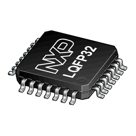
If you want the drawing for this package Then use this document number 32-pin LQFP 98ASH70029A 44-pin LQFP 98ASS23225W 64-pin QFP 98ASB42844B 64-pin LQFP 98ASS23234W KE02 Sub-Family Data Sheet, Rev3, 07/2013. Freescale Semiconductor, Inc. -
Page 31: Pinout
— — — PTD5 KBI1_P5 — — — PTC1 — FTM2_CH1 — ADC0_SE9 PTC0 — FTM2_CH0 — ADC0_SE8 — — PTF7 — — — ADC0_SE15 Table continues on the next page... KE02 Sub-Family Data Sheet, Rev3, 07/2013. Freescale Semiconductor, Inc. - Page 32 — PTC5 — FTM1_CH1 — RTCO PTC4 RTCO FTM1_CH0 ACMP0_IN2 SWD_CLK PTA5 FTM0_CLK — RESET PTA4 — ACMP0_OUT — SWD_DIO 1. This is a high-current drive pin when operated as output. KE02 Sub-Family Data Sheet, Rev3, 07/2013. Freescale Semiconductor, Inc.
-
Page 33: Device Pin Assignment
PTF3 PTH0 PTB0 PTE6 PTB1 Pins in bold are not available on less pi n-count packages. 1. High source/sink current pins 2. True open drain pins Figure 21. 64-pin QFP/LQFP packages KE02 Sub-Family Data Sheet, Rev3, 07/2013. Freescale Semiconductor, Inc. -
Page 34: Revision History
PTB0 PTB6 PTB1 1. High source/sink current pins 2. True open drain pins Figure 23. 32-pin LQFP package 9 Revision history The following table provides a revision history for this document. KE02 Sub-Family Data Sheet, Rev3, 07/2013. Freescale Semiconductor, Inc. - Page 35 Revision history Table 18. Revision history Rev. No. Date Substantial Changes 07/2013 Initial public release. KE02 Sub-Family Data Sheet, Rev3, 07/2013. Freescale Semiconductor, Inc.
- Page 36 Semiconductor, Inc., Reg. U.S. Pat. & Tm. Off. All other product or service names are the property of their respective owners. ARM and Cortex-M0+ are the registered trademarks of ARM Limited. ©2013 Freescale Semiconductor, Inc. Document Number MKE02P64M20SF0 Revision 3, 07/2013...
Need help?
Do you have a question about the *KE02 Series and is the answer not in the manual?
Questions and answers