
Related Manuals for Analog Devices MICROCONVERTER ADUC814-28TSSOP


Summary of Contents for Analog Devices MICROCONVERTER ADUC814-28TSSOP
- Page 1 C814 E VALUATION OARD EFERENCE UIDE ® ® C814 ICRO ONVERTER ™ ™ D UICK TART EVELOPMENT YSTEM...
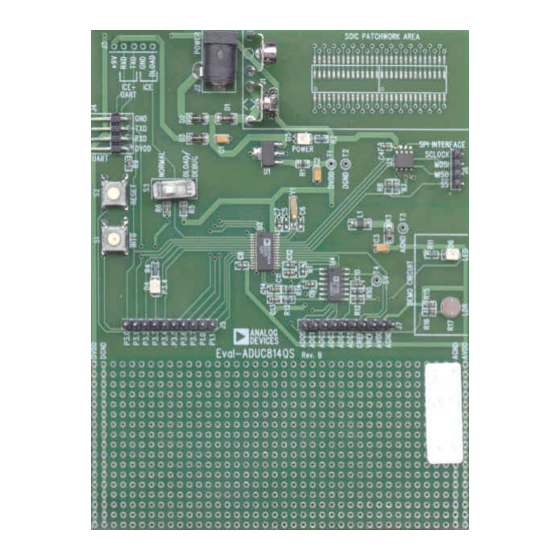
- Page 2 ADuC814 Evaluation Board Reference Guide ONTENTS Evaluation Board Reference Guide 1) Evaluation Board Overview 2) Evaluation Board Features 3) Using the LDR demo circuit 4) External Junctions (Connectors) 5) Parts List Figure 1: Reference Orientation of the ADuC814 Evaluation Board Version 1.0 (5/1/02) Page 2 of 10...
-
Page 3: Evaluation Board Overview
ADuC814 Evaluation Board Reference Guide 1.0 E VALUATION OARD VERVIEW The ADuC814 – 28TSSOP Evaluation board has the following features: • 2 Layer PCB (5” X 4” Form Factor) • 9V input power supply/9V battery connection, regulated to 5V on board •... -
Page 4: Evaluation Board Features
ADuC814 Evaluation Board Reference Guide 2.0 E VALUATION OARD EATURES Power Supply: The user should connect the 9V battery via J1(-) and J1(+). The 9V supply is regulated via a linear voltage regulator (U1). The 5V regulator output being used to drive the rest of the board directly. Alternatively a 9V supply can be fed to the board via the 2.1mm input power socket (J2). - Page 5 ADuC814 Evaluation Board Reference Guide Miscellaneous I/O: RESET Input: The reset input is driven from the push button switch to allow the user manual access to the reset button. Note: The ADuC814 reset pin is schmitt triggered internally. INT0 INT0 Input : The INT0 INT0 push button switch is located down the left side of the board beside the Reset Input.
- Page 6 ADuC814 Evaluation Board Reference Guide 3.0 U LDR C SING THE IRCUIT As can be seen from examining the schematic an example LDR circuit is connected shown in Figure 2 below: Application Code Figure 2: Circuit diagram of the LDR Circuit Using the sample code in C:\ADuC\code\adc\adcldr.asm the variation in the resistance of the ldr can be seen by the reducing brightness of the output led as the amount of light is decreased.
- Page 7 ADuC814 Evaluation Board Reference Guide 4.0 E XTERNAL UNCTIONS ONNECTORS All Ports Pins, Timer I/O and Device Interface Signals are brought out to external connection points for easy connection via the prototype area or external instruments as detailed below. J7 Analog I/O Connector The analog I/O connector J7 carries all ADC inputs and DAC output channels as well as the external and C inputs.
- Page 8 ADuC814 Evaluation Board Reference Guide J5 (SPI/I2C Connector) J5 is situated to the right side of the board and gives access to both the SPI interfaces. The orientation and pinout of the connector is given below. Function SCLOCK MOSI MISO Table 2: Pin functions for SPI connector J7 Version 1.0 (5/1/02) Page 8 of 10...
- Page 9 Part Description Supplier Cat No ZR78L05G ZETEX 5V 200mA Regulator SOT-223 Farnell 572-329 ADUC814ARU MicroConverter Analog Devices ADUC814BRU FM25640-S RAMTRON SPI FRAM Future Electronics Ltd OP491GS Quad Single Supply Rail-to-Rail Op-amp Analog Devices 0.33uF 35V SMD Tantalum Cap, Taj-A Case...
- Page 10 ADuC814 Evaluation Board ReferenceGuide S1 S2 Push button Switch SMD sealed 6mm Push Button Switch Farnell 177-807 Toggle Switch Single Pole 2 Position Slide Switch Farnell 733-647 T1 T2 T3 (Not populated) Testpoint Raised Loop Testpoint Farnell 240-345 32.768 kHz XTAL Seiko MC-306 Farnell 300-3127...
Need help?
Do you have a question about the MICROCONVERTER ADUC814-28TSSOP and is the answer not in the manual?
Questions and answers