Advertisement
Quick Links
One Technology Way • P.O. Box 9106 • Norwood, MA 02062-9106 • Tel: 781/329-4700 • Fax: 781/326-8703 •
TABLE OF CONTENTS
Evaluation Board Overview.......................................... 1
Evaluation Board Features........................................... 1
DIP Switch Link Options............................................... 2
External Connectors .................................................... 3
External Memory Interface .......................................... 5
Potentiometer Demonstration Circuit ......................... 6
Schematic .................................................................... 7
Parts List ..................................................................... 9
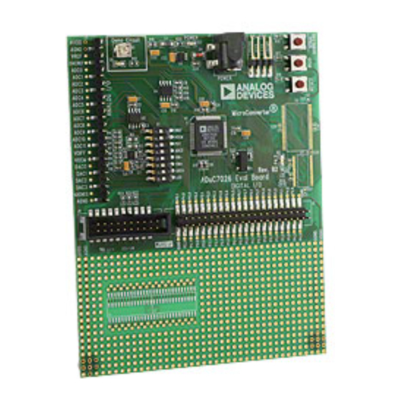
OVERVIEW
The ADuC7026 evaluation board has the following
features:
•
2-Layer PCB (4" 5" form factor)
•
9 V power supply regulated to 3.3 V on board
•
4-pin UART header to connect to RS-232 interface
cable
•
20-pin standard JTAG connector to connect to ULINK
emulator
•
Demonstration circuit
•
32.768 kHz watch crystal to drive the PLL clock
•
ADR291 2.5 V external reference chip
•
Reset/Download/IRQ0 push-buttons
•
Power indicator/general-purpose LEDs
•
Access to all ADC inputs and DAC output from external
header. All device ports are brought out to external
header pins.
•
Surface-mount and through hole general-purpose
prototype area
•
External memory and latch footprint
Notes
1. This document refers to the MicroConverter ADuC7026
Eval Board, Rev. A1.
2. All references in this document to physical orientation
of components on the board are made with respect to
a component side view of the board with the prototype
area appearing in the bottom of the board.
3. The board is laid out to minimize coupling between the
analog and digital sections of the board. To this end, the
ground plane is split with the analog section on the left-
REV. 0
ADuC7026 Evaluation Board Reference Guide
by Aude Richard
APPLICATION NOTE
hand side and a digital plane on the right-hand side of
the board. The regulated 3.3 V power supply is routed
directly to the digital section and is filtered before being
routed into the analog section of the board.
FEATURES
Power Supply
The user should connect the 9 V power supply via the
2.1 mm input power socket (J5). The input connector
is configured as CENTER NEGATIVE, i.e., GND on the
center pin and +9 V on the outer shield.
This 9 V supply is regulated via a linear voltage regulator
(U5). The 3.3 V regulator output is used to drive the digital
side of the board directly. The 3.3 V supply is also filtered
and then used to supply the analog side of the board.
When on, the red LED (D3) indicates that a valid 3.3 V
supply is being driven from the regulator circuit. All
active components are decoupled with 0.1 F at device
supply pins to ground.
RS-232 Interface
The ADuC7026 (U1) P1.1 and P1.0 lines are connected to
the RS-232 interface cable via connector (J1). The interface
cable generates the required level shifting to allow direct
connection to a PC serial port. Ensure that the cable
supplied is connected to the board correctly, i.e., DVDD is
connected to DVDD and DGND is connected to DGND.
Emulation Interface
Nonintrusive emulation and download are possible on the
ADuC7026 via JTAG by connecting the ULINK emulator to
the J4 connector.
Crystal Circuit
The board is fitted with a 32.768 kHz crystal, from which
the on-chip PLL circuit can generate a 45 MHz clock.
External Reference (ADR291)
The external 2.5 V reference chip (U2) has two functions.
It is provided on the evaluation board to demonstrate the
external reference option of the ADuC7026, but its main
purpose is to generate the V
amplifier, if required.
Reset/Download/IRQ0 Push-buttons
A RESET push-button is provided to allow the user to
manually reset the part. When inserted, the RESET pin
of the ADuC7026 will be pulled to DGND. Because the
AN-744
www.analog.com
voltage of the differential
OCM
Advertisement

Related Manuals for Analog Devices ADuC7026


Summary of Contents for Analog Devices ADuC7026
-
Page 1: Table Of Contents
RS-232 Interface • Demonstration circuit The ADuC7026 (U1) P1.1 and P1.0 lines are connected to • 32.768 kHz watch crystal to drive the PLL clock the RS-232 interface cable via connector (J1). The interface cable generates the required level shifting to allow direct •... -
Page 2: Dip Switch Link Options
A general-purpose LED Table 1. (D2) is directly connected to P4.2 of the ADuC7026. When Table 1. V Range P4.2 is cleared the LED will be turned on, and when P4.2 is set, the LED will be turned off. -
Page 3: External Connectors
J4 provides a connection of the evaluation board to the The analog I/O connector J3 provides external connections PC via a USB cable and ULINK provided in the ADuC7026 for all ADC inputs, reference inputs, and DAC outputs. The Development System. - Page 4 AN-744 Table 3. Pin Functions for Digital I/O Connector J2 Pin Number Pin Description Pin Number Pin Description J2-1 DGND J2-22 P2.0 CONV/SOUT/PLAO[5] J2-2 P4.5 J2-23 P0.5 AD13/PLAO[13] IRQ1/ADC /MS0/PLAO[2] BUSY J2-3 P4.4 J2-24 P0.4 AD12/PLAO[12] IRQ0/PWM /MS1/PLAO[1] TRIP J2-4 P4.3 J2-25 P3.5...
-
Page 5: External Memory Interface
16 bits of data AD[15 - 0] are directly con- EXTERNAL MEMORY INTERFACE A footprint for a 32 kB 16 SRAM is provided on board nected from the ADuC7026 to the memory. as well as a footprint for a 16 -bit D-latch since address Addresses: and data are multiplexed on the external bus. -
Page 6: Potentiometer Demonstration Circuit
AN-744 POTENTIOMETER DEMONSTRATION CIRCUIT Using the sample code in \adc\pot.c, the variation in �� �� the potentiometer resistance can be seen on the output �� �� LED. ��� ��� Note that the internal and external references are 2.5 V, which gives an ADC input range of 0 V to 2.5 V in single- ended mode. -
Page 7: Schematic
AN-744 SCHEMATIC ������� ��������� ������ ��������� ���� ��������� Figure 4. ADuC7026 Evaluation Board Schematic REV. 0 –7–... - Page 8 AN-744 Figure 5. ADuC7026 Evaluation Board Silkscreen –8– REV. 0...
-
Page 9: Parts List
AN-744 Table 4. ADuC7026 Evaluation Board Parts List Component Part Description Order Number Order From EVAL- ADuC7026QS QuickStart PCB 1 PCB-1 2-sided surface-mount PCB PCB Standoff Standoff Stick on mounting feet 148-922 Farnell ADuC7026 MicroConverter (80 LQFP) ADuC7026CP ADR291 Band gap reference... - Page 10 AN-744 Table 4. ADuC7026 Evaluation Board Parts List (Continued) Component Part Description Order Number Order From R13, R14 0 Surface-mount resistor, 772-227 Farnell 0603 case R15–R18 1 k Surface-mount resistor, 911-239 Farnell 0603 case 1.5 Surface-mount resistor, 758-267...
- Page 11 –11–...
- Page 12 C Patent Rights to use these components in an I C system, provided that the system conforms to the I C Standard Specification as defined by Philips. © 2004 Analog Devices, Inc. All rights reserved. Trademarks and registered trademarks are the property of their respective owners. –12–...
Need help?
Do you have a question about the ADuC7026 and is the answer not in the manual?
Questions and answers