
Subscribe to Our Youtube Channel
Related Manuals for ADLINK Technology PCIe-9529


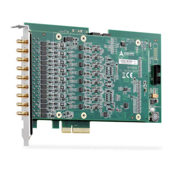
Summary of Contents for ADLINK Technology PCIe-9529
- Page 1 PCIe-9529 8-CH 24-Bit 192 kS/s Dynamic Signal Acquisition Module User’s Manual Manual Rev.: 2.00 Revision Date: July 11, 2014 Part Number: 50-11255-1000 Advance Technologies; Automate the World.
- Page 2 Revision History Revision Release Date Description of Change(s) 2.00 July 11, 2014 Initial Release...
- Page 3 PCIe-9529 Preface Copyright 2014 ADLINK Technology, Inc. This document contains proprietary information protected by copy- right. All rights are reserved. No part of this manual may be repro- duced by any mechanical, electronic, or other means in any form without prior written permission of the manufacturer.
- Page 4 Additional information, aids, and tips that help users perform tasks. NOTE: NOTE: Information to prevent minor physical injury, component dam- age, data loss, and/or program corruption when trying to com- plete a task. CAUTION: Information to prevent serious physical injury, component damage, data loss, and/or program corruption when trying to complete a specific task.
-
Page 5: Table Of Contents
PCIe-9529 Table of Contents Preface ..................iii List of Figures ............... vii List of Tables................ix 1 Introduction ................ 1 Features................1 Applications ................. 1 Specifications............... 2 1.3.1 Analog Input ............... 2 1.3.2 Timebase..............9 1.3.3 Triggers ..............9 1.3.4 General Specifications.......... - Page 6 Trigger Source and Trigger Modes ........22 Trigger Mode..............25 ADC Timing Control ............27 3.5.1 Timebase ..............27 3.5.2 DDS Timing vs. ADC ..........27 3.5.3 Filter Delay in ADC ........... 27 Synchronizing Multiple Modules ........28 3.6.1 SSI_TIMEBASE............29 3.6.2 SSI_SYNC_START ..........
-
Page 7: List Of Figures
Figure 1-4: Spurious Free Dynamic Range 108kS/s ....8 Figure 1-5: Spurious Free Dynamic Range 192kS/s ....8 Figure 1-6: PCIe-9529 Side View ..........11 Figure 1-7: PCIe-9529 I/O Array ..........12 Figure 3-1: Analog Input Architecture ......... 17 Figure 3-2: Linked List of PCI Address DMA Descriptors ... - Page 8 This page intentionally left blank. viii List of Figures...
-
Page 9: List Of Tables
PCIe-9529 List of Tables Table 1-1: Timebase ................. 9 Table 1-2: Trigger Source & Mode............ 9 Table 1-3: Digital Trigger Input ............9 Table 3-1: Input Range and Data Format ........19 Table 3-2: Input Range Midscale Values ........19 Table 3-3: ADC Sample Rates vs DDS Output Clock..... - Page 10 This page intentionally left blank. List of Tables...
-
Page 11: Introduction
PCIe-9529 Introduction The PCIe-9529 is a high-performance 8-CH 24-Bit 192 kS/s dynamic signal acquisition module, specifically designed for appli- cations such as structural health monitoring, noise, vibration, and harshness (NVH) measurement, and phased array data acquisi- tion. The PCIe-9529 features 24-bit simultaneous sampling at 192 kS/s... -
Page 12: Specifications
1.3 Specifications 1.3.1 Analog Input Channel Characteristics Channels Type Differential or pseudo-differential Coupling AC or DC, software selectable AC coupling cutoff 0.5Hz frequency ADC resolution 24-Bit ADC type Delta-sigma Input signal range ±10V, ±1V 8 kS/s to 192 kS/s, 768 μS/s increments for Fs > 108 kS/s, Sampling rate (FS) 576 μS/s increments for 54 kS/s ≤... - Page 13 PCIe-9529 System Noise Sample Rate (kS/s) System Noise1 (LSB Fs = 54 kS/s 37.4 Fs = 108 kS/s 66.5 Fs = 192 kS/s 74.6 1. Shorted input Common Mode Rejection Ratio (CMRR) Input Range (V) CMRR (dB) ±1V ±10V 1. Input frequency < 1 kHz...
- Page 14 Spurious Free Dynamic Range (SFDR) SFDR (dBc) Input Range (V) Fs = 54 kS/s Fs = 108 kS/s Fs = 192 kS/s ±1V, ±10V 1. 1 kHz input tone and -1 dBFS input amplitude. 2. Measurement Includes harmonics. Dynamic Range Dynamic Range (dBFS) Input Range (V) Fs = 54 kS/s...
- Page 15 PCIe-9529 Total Harmonic Distortion plus noise (THD+N) THD+N (dBc) 54 kS/s 108 kS/s 192 kS/s Input Range (V) 20 Hz to 22 kHz 20 Hz to 45 kHz 20 Hz to 42 kHz ±1V ±10V 1. 1 kHz input tone and -1 dBFS input amplitude...
-
Page 16: Figure 1-1: Analog Input Channel Bandwidth, -1Dbfs 108Ks/S
Interchannel Phase Mismatch Input Range (V) Phase Mismatch (°) 1 khz 20 khz 86.4 khz ±1V, ±10V 0.442 1.64 1. -1 dBFS input amplitude Magnitude Response −5 −10 −15 −20 −25 Frequency (Hz) Figure 1-1: Analog Input Channel Bandwidth, -1dBFS 108kS/s Introduction... -
Page 17: Figure 1-2: Analog Input Channel Bandwidth, -1Dbfs 108Ks/S
PCIe-9529 Response when AC coupling enabled −0.5 −1 −1.5 −2 −2.5 −3 −3.5 −4 −4.5 −1 Frequency (Hz) Figure 1-2: Analog Input Channel Bandwidth, -1dBFS 108kS/s SFDR 54 kS/s (1V Input Range, −1 dBFS and 1 kHz Sine Wave Input) −20... -
Page 18: Figure 1-4: Spurious Free Dynamic Range 108Ks/S
SFDR 108 kS/s (1V Input Range, −1 dBFS and 1 kHz Sine Wave Input) −20 −40 −60 −80 −100 −120 −140 −160 Frequency (Hz) x 10 Figure 1-4: Spurious Free Dynamic Range 108kS/s SFDR 192 kS/s (1V Input Range, −1 dBFS and 1 kHz Sine Wave Input) −20 −40 −60... -
Page 19: Timebase
PCIe-9529 1.3.2 Timebase Sampling Clock Internal: onboard synthesizer (10 MHz, accuracy Sampling Clock < ± 25ppm) Timebase External: SSI Delay Trigger Timebase PCIe clock (125 MHz) Table 1-1: Timebase 1.3.3 Triggers Trigger Source & Mode Trigger source Software, external digital trigger, analog trigger, and SSI... - Page 20 Temperature: 0°C - 55°C Operating Relative humidity: 10% - 90%, non-condensing Temperature: -20°C - +80°C Storage Relative humidity: 10% - 90%, non-condensing Calibration Onboard reference +5.000 V Temperature coefficient < 5.0 ppm/°C Warm-up time 15 minutes Power Consumption Power Rail Standby Current (mA) Full Load (mA) +3.3 V...
-
Page 21: Schematics And I/O
PCIe-9529 1.4 Schematics and I/O All dimensions are in mm NOTE: NOTE: 100.36 59.05 176.42 Figure 1-6: PCIe-9529 Side View Introduction... -
Page 22: Figure 1-7: Pcie-9529 I/O Array
The PCIe-9529 I/O array is labeled to indicate connectivity, as shown. Figure 1-7: PCIe-9529 I/O Array Introduction... -
Page 23: Software Support
PCIe-9529 1.5 Software Support ADLINK provides versatile software drivers and packages to suit various user approaches to building a system. Aside from pro- gramming libraries, such as DLLs, for most Windows-based sys- tems, ADLINK also provides drivers for other application ®... - Page 24 This page intentionally left blank. Introduction...
-
Page 25: Getting Started
Flat-head screwdriver Anti-static wrist strap Antistatic mat ADLINK PCIe-9529 DSA modules are electrostatically sensitive and can be easily damaged by static electricity. The module must be handled on a grounded anti-static mat. The operator must wear an anti-static wristband, grounded at the same point as the anti-static mat. -
Page 26: Installing The Module
Inspect the carton and packaging for damage. Shipping and han- dling could cause damage to the equipment inside. Make sure that the equipment and its associated components have no damage before installation. The equipment must be protected from static discharge and physical shock. -
Page 27: Operations
PCIe-9529 Operations This chapter contains information regarding analog input, trigger- ing and timing for the PCIe-9529. 3.1 Functional Block Diagram JFET Buffer Quad OPAMP 24bit ADC SSI Bus [0..7] 2-bit /12.288MHz ADC Ctrl PCIe Controller 10 MHz PCIe Gen1 Reference &... - Page 28 The corner frequency (-3dB) is about 0.5Hz. Input for IEPE For applications that require sensors such as accelerometers or microphones, the PCIe-9529 provides an excitation current source. The common excitation current is usually about 4mA for these IEPE sensors. A DC voltage offset is generated due to the excitation current and sensor impedance.
-
Page 29: Input Range And Data Format
A/D conversion, A/D data is buffered in a Data FIFO, and can then be transferred to PC memory for further processing. Transfer characteristics of the two input ranges of the PCIe-9529 are as follows. Data format of the PCIe-9529 is 2’s complement. Least Full-scale... -
Page 30: Dma Data Transfer
3.2.4 DMA Data Transfer The PCIe-9529, as a PCIe Gen1 X 4 device, provides a 192KS/s sampling rate ADC, generating a 3.072 MByte/second rate. To provide efficient data transfer, a PCI bus-mastering DMA is essen- tial for continuous data streaming, as it helps to achieve the full potential PCI Express bus bandwidth. -
Page 31: Figure 3-2: Linked List Of Pci Address Dma Descriptors
PCIe-9529 ing OS, such as Microsoft Windows, Linux, or other, it is difficult to allocate a large continuous memory block. Therefore, the bus con- troller provides DMA transfer with scatter-gather function to link non-contiguous memory blocks into a linked list to enable transfer of large amounts of data without memory limitations. -
Page 32: Trigger Source And Trigger Modes
Analog CH7 SSI_AD_TRIG Figure 3-3: Trigger Architecture The PCIe-9529 requires a trigger to implement acquisition of data. Configuration of triggers requires identification of trigger source. The PCIe-9529 supports internal software trigger, external digital trigger and SSI Bus Number 5 as well as analog trigger. -
Page 33: Figure 3-4: External Digital Trigger
Figure 3-4: External Digital Trigger SSI_AD_TRIG The PCIe-9529 utilizes SSI Bus Number 5 to act as a System Synchronization Interface (SSI). With the interconnected bus provided by SSI Bus, multiple modules are easily synched. When configured as input the PCIe-9529 serves as a slave module and can accept trigger signals from SSI Bus Number 5, asserted from other PCIe-9529 modules. -
Page 34: Figure 3-5: Analog Trigger Conditions
the specified trigger level to a voltage exceeding the specified trigger level. Negative-slope trigger: The trigger event occurs when the analog input signal changes from a voltage exceed- ing the specified trigger level to a voltage lower than the specified trigger level. Positive-Slope Trigger Event Negative-Slope Trigger Occurs... -
Page 35: Trigger Mode
PCIe-9529 Trigger Export The PCIe-9529 utilizes SSI Bus Number 5 to act as a System Synchronization Interface (SSI). With the interconnected bus provided by SSI Bus, multiple modules are easily synched. When configured as input the PCIe-9529 serves as a slave module and can accept trigger signals from SSI Bus Number 5, asserted from other PCIe-9529 modules. -
Page 36: Figure 3-7: Delay Trigger Mode Acquisition
Post-trigger or delay trigger acquisition with re-trigger function enables collection of data after several trigger events, as shown. When the number of triggers is defined, the PCIe-9529 acquires specific sample data each time a trigger is accepted. All sampled data is stored in onboard memory first, until all trig-... -
Page 37: Adc Timing Control
PCIe-9529 3.5 ADC Timing Control 3.5.1 Timebase Onboard Oscillator SYNC_CLK SSI_TIMEBASE ADC0_CLK ADC1_CLK SSI_TIMEBASE FPGA_MCLK Figure 3-9: Timebase Architecture An onboard timebase clock drives the sigma-delta ADC, with fre- quency exceeding the sample rate and produced by a PLL chip, with output frequency programmable to superior resolution. -
Page 38: Synchronizing Multiple Modules
CN4, labeled SSI Bus [0:7] pro- vide a flexible interface for synching multiple modules with the requirement of cabling. The PCIe-9529 utilizes the SSI Bus [0:7] as a System Synchronization Interface (SSI). Dedicate routing of timebase clock and trigger signals onto the SSI Bus enables the PCIe-9529 to simplify synchronization between multiple modules. -
Page 39: Ssi_Timebase
3.6.1 SSI_TIMEBASE As output, the SSI_TIMEBASE signal transmits the onboard ADC timebase through the SSI bus. As input, the PCIe-9529 accepts the SSI_TIMEBASE signal as the source of the timebase. 3.6.2 SSI_SYNC_START Before a SSI master issues SSI_AD_TRIG to other SSI slaves,... -
Page 40: Ssi_Ad_Trig
SSI_AD_TRIG As output, the SSI_AD_TRIG signal reflects the trigger event sig- nal in an acquisition sequence. As input, the PCIe-9529 accepts the SSI_AD_TRIG signal as the trigger event source. The signal is configured in the rising edge-detection mode, with minimum pulse width 20ns. -
Page 41: A Appendix: Calibration
This chapter introduces the calibration process to minimize analog input measurement errors. A.1 Calibration Constant The PCIe-9529 is factory calibrated before shipment, with associ- ated calibration constants written to the onboard EEPROM. At system boot, the PCIe-9529 driver loads these calibration con- stants, such that analog input path errors are minimized. - Page 42 Before initializing auto-calibration, it is recommended to warm up the PCIe-9529 for at least 20 minutes and remove connected cables. It is not necessary to manually factor delay into applications, as the PCIe-9529 driver automatically adds the compensation time. NOTE:...
-
Page 43: Important Safety Instructions
PCIe-9529 Important Safety Instructions For user safety, please read and follow all instructions, WARNINGS, CAUTIONS, and NOTES marked in this manual and on the associated equipment before handling/operating the equipment. Read these safety instructions carefully. Keep this user’s manual for future reference. - Page 44 Never attempt to fix the equipment. Equipment should only be serviced by qualified personnel. A Lithium-type battery may be provided for uninterrupted, backup or emergency power. Risk of explosion if battery is replaced with an incorrect type; please dispose of used batteries appropriately. WARNING: Equipment must be serviced by authorized technicians when:...
-
Page 45: Getting Service
5215 Hellyer Avenue, #110, San Jose, CA 95138, USA Tel: +1-408-360-0200 Toll Free: +1-800-966-5200 (USA only) Fax: +1-408-360-0222 Email: info@adlinktech.com ADLINK Technology (China) Co., Ltd. Address: (201203) 300 Fang Chun Rd., Zhangjiang Hi-Tech Park, Pudong New Area, Shanghai, 201203 China Tel: +86-21-5132-8988 Fax:... - Page 46 84 Genting Lane #07-02A, Cityneon Design Centre, Singapore 349584 Tel: +65-6844-2261 Fax: +65-6844-2263 Email: singapore@adlinktech.com ADLINK Technology Singapore Pte. Ltd. (Indian Liaison Office) Address: 1st Floor, #50-56 (Between 16th/17th Cross) Margosa Plaza, Margosa Main Road, Malleswaram, Bangalore-560055, India Tel: +91-80-65605817, +91-80-42246107 Fax: +91-80-23464606 Email: india@adlinktech.com...
Need help?
Do you have a question about the PCIe-9529 and is the answer not in the manual?
Questions and answers