Sign In
Upload
Manuals
Brands
ADLINK Technology Manuals
Control Unit
PCIe-9529
ADLINK Technology PCIe-9529 Manuals
Manuals and User Guides for ADLINK Technology PCIe-9529. We have
1
ADLINK Technology PCIe-9529 manual available for free PDF download: User Manual
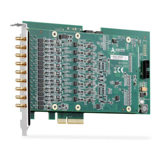
ADLINK Technology PCIe-9529 User Manual (46 pages)
8-CH 24-Bit 192 kS/s Dynamic Signal Acquisition Module
Brand:
ADLINK Technology
| Category:
Control Unit
| Size: 1 MB
Table of Contents
Table of Contents
5
List of Figures
7
List of Tables
9
1 Introduction
11
Features
11
Applications
11
Specifications
12
Analog Input
12
Figure 1-1: Analog Input Channel Bandwidth, -1Dbfs 108Ks/S
16
Figure 1-2: Analog Input Channel Bandwidth, -1Dbfs 108Ks/S
17
Figure 1-3: Spurious Free Dynamic Range 54Ks/S
17
Figure 1-4: Spurious Free Dynamic Range 108Ks/S
18
Figure 1-5: Spurious Free Dynamic Range 192Ks/S
18
Timebase
19
Triggers
19
General Specifications
19
Table 1-1: Timebase
19
Table 1-2: Trigger Source & Mode
19
Table 1-3: Digital Trigger Input
19
Schematics and I/O
21
Figure 1-6: Pcie-9529 Side View
21
Figure 1-7: Pcie-9529 I/O Array
22
Software Support
23
Sdk
23
Dsa-Dask
23
2 Getting Started
25
Package Contents
25
Installation Environment
25
Installing the Module
26
3 Operations
27
Functional Block Diagram
27
Analog Input Channel
27
Analog Input Front-End Configuration
27
Figure 3-1: Analog Input Architecture
27
Input Range and Data Format
29
ADC and Analog Input Filter
29
Table 3-1: Input Range and Data Format
29
Table 3-2: Input Range Midscale Values
29
DMA Data Transfer
30
Table 3-3: ADC Sample Rates Vs DDS Output Clock
30
Figure 3-2: Linked List of PCI Address DMA Descriptors
31
Trigger Source and Trigger Modes
32
Figure 3-3: Trigger Architecture
32
Figure 3-4: External Digital Trigger
33
Figure 3-5: Analog Trigger Conditions
34
Table 3-4: Preferred Characteristics for Analog Triggers
34
Trigger Mode
35
Figure 3-6: Post-Trigger Acquisition
35
Figure 3-7: Delay Trigger Mode Acquisition
36
Figure 3-8: Re-Trigger Mode Acquisition
36
ADC Timing Control
37
Timebase
37
DDS Timing Vs. ADC
37
Filter Delay in ADC
37
Figure 3-9: Timebase Architecture
37
Table 3-5: Timing Relationship between ADC and PLL Clock
37
Synchronizing Multiple Modules
38
Table 3-6: ADC Filter Delay
38
Table 3-7: SSI Timing Signal Definitions
38
Figure 3-10: SSI Architecture
39
Ssi_Sync_Start
39
Ssi_Timebase
39
Ssi_Ad_Trig
40
A Appendix: Calibration
41
Calibration Constant
41
Auto-Calibration
41
A.1 Calibration Constant
41
Important Safety Instructions
43
Getting Service
45
Advertisement
Advertisement
Related Products
ADLINK Technology PXI-8164
ADLINK Technology PCI-8164
ADLINK Technology PXI-7901
ADLINK Technology PXI-7931
ADLINK Technology PXI-7921
ADLINK Technology PCIe-9842
ADLINK Technology PCIe-9834
ADLINK Technology PCIe-9834P
ADLINK Technology NuDAQ PCIe-9100 Series
ADLINK Technology NuDAQ PCIe-9101
ADLINK Technology Categories
Computer Hardware
Motherboard
PCI Card
Control Unit
Desktop
More ADLINK Technology Manuals
Login
Sign In
OR
Sign in with Facebook
Sign in with Google
Upload manual
Upload from disk
Upload from URL