Table of Contents
Advertisement
Quick Links
Introduction
The evaluation board is designed to help the customer evaluate the
devices in IDT's Timing portfolio. When the board is connected to a PC running IDT
device can be configured and programmed to generate different combinations of frequencies.
Board Overview
Use
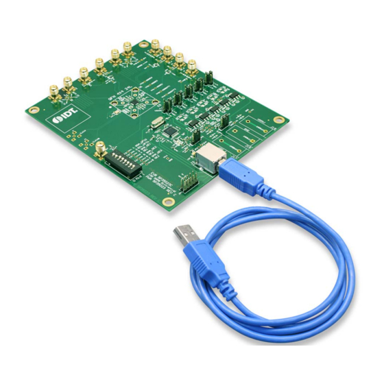
Figure 1
and
Table 1
to identify: USB connector and the input and output frequency SMA connectors.
Figure 1. EVK5P35023 Evaluation Board
4
3
2
1
5
©2017 Integrated Device Technology, Inc.
®
VersaClock
3S - 5P35023 Evaluation Board
A
5P35023
device, the latest addition to the family of programmable
Timing
C
B
1
User Manual
Commander™ software through a USB, the
D
E
F
G
H
I
J
June 8, 2017
Advertisement
Table of Contents

Subscribe to Our Youtube Channel
Related Manuals for IDT VersaClock 3S


Summary of Contents for IDT VersaClock 3S
-
Page 1: User Manual
The evaluation board is designed to help the customer evaluate the 5P35023 device, the latest addition to the family of programmable devices in IDT's Timing portfolio. When the board is connected to a PC running IDT Timing Commander™ software through a USB, the device can be configured and programmed to generate different combinations of frequencies. -
Page 2: Board Power Supply
This crystal is used as a reference source for the clock signal. USB Connector Connect this USB to your PC to run IDT Timing Commander. This can be a differential pair, or two single-ended outputs. By default, Differential Output #2 DIFF_T2/C2 it’s an LPHCSL differential output. -
Page 3: Output Clock Voltages
® VersaClock 3S - 5P35023 Evaluation Board User Manual Figure 2. JP5 Jumper Position (pins 1 & 2) for the On-Board Voltage Regulators Jumping to the pin configuration as shown will select the power source from on-board voltage regulators powered by USB. Output Clock Voltages Like V and V... -
Page 4: On-Board Crystal
® VersaClock 3S - 5P35023 Evaluation Board User Manual Figure 4. Connecting the Board with USB Port for Communications with Timing Commander Software On-board Crystal A 25MHz crystal is installed on the board and is used as a source for reference frequency. Board Default Frequency Output Table 2. - Page 5 Follow the “Getting Started Steps” in Timing Commander An I C connection is established between GUI software software. and VersaClock 3S device. Using the Timing Commander GUI, start a new settings Configure the Timing Commander software for the file, or open a pre-optimized file.
-
Page 6: Evaluation Board Schematics
® VersaClock 3S - 5P35023 Evaluation Board User Manual Evaluation Board Schematics Evaluation board schematics are shown on the following pages. Figure 5. Evaluation Board Schematic (1) VDDD VBAT_PS VDDD VDDA VDDA_VDDD1 5P53023 1,3,4 VDDSE1 VDDSE1 1,3,4 1,3,4 VDDSE1 VDDSE2 VDDA VDDSE1 SER1... - Page 7 ® VersaClock 3S - 5P35023 Evaluation Board User Manual Figure 6. Evaluation Board Schematic (2) FB1_JP8 3V3_USB AADVARK USB_5V BLM18AG601SN1D C3 10nF SCL_AARDVARK TP12 VDDO_J Node#1 SDA_AARDVARK C4 0.1 uF 10 uF TP13 C5 0.1 uF Header_10Pin BLM18AG601SN1D Node#2 C7 10 uF C8 10 uF Header_3Pin SCL_DFC1...
- Page 8 ® VersaClock 3S - 5P35023 Evaluation Board User Manual Figure 7. Evaluation Board Schematic (3) SE_4 VDDSE1 INV_OE1 VDDSE1 0_NP SMA_OE1 CON SMA4 4.7pF_NP 200K_NP OE_R1 CON2_NP 0_NP SE_1 TC7SZ125FE CON SMA4 0_NP 200K SMA_OE1 VDDSE2 CON SMA4 INV_OE2 VDDSE2 4.7pF_NP CON2_NP 200K...
- Page 9 ® VersaClock 3S - 5P35023 Evaluation Board User Manual Figure 8. Evaluation Board Schematic (4) VDDSE1 VDDSE2 VDDSE3 USB_5V VDDDIFF1 VDD1_1.8V VDDDIFF2 USB_5V USB_5V 10 uF 10 uF 243_1% VDDA_VDDD1 LM317A/SO-223 VDDA_VDDD1 VADJ_VDD1 107_1% 10 uF POT_500 VDD1_1.8V VDD2_2.5V VDD1_1.8V TP21 VDD2_2.5V VDD3_3.3V...
-
Page 10: Signal Termination Options
® VersaClock 3S - 5P35023 Evaluation Board User Manual Signal Termination Options Termination options for differential output 1–2 in the evaluation board are displayed in Figure 9. The termination circuits are designed to optionally terminate the output clocks in LVPECL, LVDS, LVCMOS and HCSL signal types by populating (or not-populating) some resistors. -
Page 11: Ordering Information
Note: **The differential output is applicable to LPHCSL which is the default configuration of the board. *The single-ended output is applicable to LVCMOS which is the default configuration of the board. Contact IDT if user wants to change termination configuration to support other output signal types. Ordering Information Table 12. -
Page 12: Revision History
IDT or any third parties. IDT's products are not intended for use in applications involving extreme environmental conditions or in life support systems or similar devices where the failure or malfunction of an IDT product can be rea- sonably expected to significantly affect the health or safety of users.
Need help?
Do you have a question about the VersaClock 3S and is the answer not in the manual?
Questions and answers