Table of Contents
Advertisement
Quick Links
Introduction
®
The VersaClock
6E programmer board is made to ease the programming of blank 5P49V6965 or 5P49V6975 devices. With the
on-board USB interface, the IDT
for configuration and programming of its OTP memory.
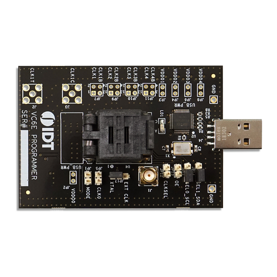
Board Overview
Use
Figure 1
and
Table 1
to identify board items and features.
Figure 1. Programmer Board Overview
10
9
©2019 Integrated Device Technology, Inc.
®
VersaClock
6E – 5P49V6965 and 5P49V6975
Programmer Board User Guide
Timing
Commander™ GUI can be used to communicate with the VersaClock
11
5
6
8
7
12
3
4
1
®
6E device in the socket
13
1
2
June 17, 2019
Advertisement
Table of Contents

Related Manuals for IDT VersaClock 6E 5P49V6965


Summary of Contents for IDT VersaClock 6E 5P49V6965
-
Page 1: Board Overview
The VersaClock 6E programmer board is made to ease the programming of blank 5P49V6965 or 5P49V6975 devices. With the ® on-board USB interface, the IDT Timing Commander™ GUI can be used to communicate with the VersaClock 6E device in the socket for configuration and programming of its OTP memory. -
Page 2: Connecting The Board To A Computer
® VersaClock 6E – 5P49V6965 and 5P49V6975 Programmer Board User Guide Table 1. 5P49V6965/5P49V6975 Programmer Board Pins and Functions Label Number Name On-board Connector Label Function USB connector. I2C / SEL JP14, JP16 Jumpers to connect I2C or control SEL0/1. OE / CLKSEL JP12, JP13 Jumpers to control OE and CLKSEL. - Page 3 ® VersaClock 6E – 5P49V6965 and 5P49V6975 Programmer Board User Guide Figure 3. JP14 and JP16 for I2C Figure 4. JP14 and JP16 for SEL0/1 After programming multiple configurations, the 5P49V6965/6975 can be restarted in Hardware Select mode and then the SEL0 and SEL1 pins can be used to select a configuration.
-
Page 4: Jp12 And Jp13 Functionality
® VersaClock 6E – 5P49V6965 and 5P49V6975 Programmer Board User Guide JP12 and JP13 Functionality JP12 controls the CLKSEL pin and JP13 controls the SD/OE pin on the 5P49V6965/6975. These pins have pull-down resistors on the chip so when the pins are left open, the pins will be pulled low. When placing a jumper, the pin will be pulled high. This way the functionality of the CLKSEL and SD/OE pins can be verified. -
Page 5: Jp1 And Jp5 Functionality
® VersaClock 6E – 5P49V6965 and 5P49V6975 Programmer Board User Guide JP1 and JP5 Functionality JP5 is the CLK0 output (OUT0) of the 5P49V6965/6975. The upper pin is ground and the lower pin is the actual output. Connect a probe between the upper (GND) and lower (OUT0) pins to measure the OUT0 frequency or waveform. -
Page 6: J2 And J3 Functionality
® VersaClock 6E – 5P49V6965 and 5P49V6975 Programmer Board User Guide J2 and J3 Functionality J2 and J3 are SMA footprints for an alternative differential connection to OUT1. The default programmer board does not have these connectors assembled. Figure 9. J2 and J3 Alternative CLK1 (OUT1) JP3, JP4, JP6 and JP8 Functionality The default programmer board does not have jumper pins assembled for JP3, JP4, JP6 and JP8. -
Page 7: Configuration And Setup
® VersaClock 6E – 5P49V6965 and 5P49V6975 Programmer Board User Guide Configuration and Setup Use the following steps to setup the 5P49V6965 or 5P49V6975 device using USB-to-I2C and start the configuration. 1. Before connecting the programmer board to USB, make sure JP1 is open (no jumper). Also see JP1 functionality and Figure 7. 2. - Page 8 ® VersaClock 6E – 5P49V6965 and 5P49V6975 Programmer Board User Guide 11. After finishing the burning to OTP, the device can be tested as follows: • Unplug USB to remove power. • Place JP1 to make the device start in Hardware Select mode the next time USB (power) is plugged in again. •...
- Page 9 ® VersaClock 6E – 5P49V6965 and 5P49V6975 Programmer Board User Guide Figure 12. 5P49V6965/6975 Programmer Board Schematics – page 2 10nF USB_5V 0.1uF 600 ohm 500mA 0.1uF Green VCC2232 10uF VCC2232_3V VBUS 3V3_USB 3V3_USB 0.1uF 0.047uF USB_A SEL0_SCL 3V3OUT TCK/SK TDI/DO SEL1_SDA...
-
Page 10: Ordering Information
IDT or any third parties. IDT's products are not intended for use in applications involving extreme environmental conditions or in life support systems or similar devices where the failure or malfunction of an IDT product can be rea- sonably expected to significantly affect the health or safety of users.
Need help?
Do you have a question about the VersaClock 6E 5P49V6965 and is the answer not in the manual?
Questions and answers