Table of Contents
Advertisement
Quick Links
Nexys 3™ FPGA Board Reference Manual
Revised April 11, 2016
This manual applies to the Nexys 3 rev. B
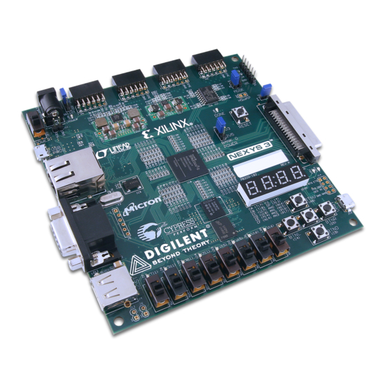
Overview
The Nexys 3 is a complete, ready-to-use digital circuit development platform based on the Xilinx Spartan-6 LX16
FPGA. The Spartan-6 is optimized for high performance logic, and offers more than 50% higher capacity, higher
performance, and more resources as compared to the Nexys 2's Spartan-3 500E FPGA.
In addition to the Spartan-6 FPGA, the Nexys 3 offers an improved collection of peripherals including 32Mbytes of
Micron's latest Phase Change nonvolatile memory, a 10/100 Ethernet PHY, 16Mbytes of Cellular RAM, a USB-
UART port, a USB host port for mice and keyboards, and an improved high-speed expansion connector. The large
FPGA and broad set of peripherals make the Nexys 3 board an ideal host for a wide range of digital systems,
including embedded processor designs based on Xilinx's MicroBlaze.
Nexys 3 is compatible with all Xilinx CAD tools, including ChipScope, EDK, and the free WebPack. The Nexys 3 uses
Digilent's newest Adept USB2 system that offers FPGA and ROM programming, automated board tests, virtual I/O,
and simplified user-data transfer facilities.
A comprehensive collection of board support IP and reference designs, and a large collection of add-on boards are
available on the Digilent website. Please see the Nexys 3 page at
DOC#: 502-182
Other product and company names mentioned may be trademarks of their respective owners.
Features include:
Xilinx Spartan-6 LX16 FPGA in a 324-pin BGA
package
16Mbyte Cellular RAM (x16)
16Mbytes SPI (quad mode) PCM non-volatile
memory
16Mbytes parallel PCM non-volatile memory
10/100 Ethernet PHY
On-board USB2 port for programming & data
xfer
USB-UART and USB-HID port (for
mouse/keyboard)
8-bit VGA port
100MHz CMOS oscillator
72 I/Os routed to expansion connectors
GPIO includes 8 LEDs, 5 buttons,8 slide
switches and 4-digit seven-segment display
USB2 programming cable included
www.digilentinc.com
Copyright Digilent, Inc. All rights reserved.
1300 Henley Court
Pullman, WA 99163
509.334.6306
www.digilentinc.com
for more information.
Page 1 of 22
Advertisement
Table of Contents

Related Manuals for Digilent Nexys 3


Summary of Contents for Digilent Nexys 3
- Page 1 UART port, a USB host port for mice and keyboards, and an improved high-speed expansion connector. The large FPGA and broad set of peripherals make the Nexys 3 board an ideal host for a wide range of digital systems, including embedded processor designs based on Xilinx's MicroBlaze.
- Page 2 Nexys 3™ FPGA Board Reference Manual Spartan-6 LX16 features include: Adept USB2 USB HID Host Config & data Mouse/Keyboard 2,278 slices each containing four 6-input LUTs Cellular RAM and eight flip-flops 16MByte USB-UART 576Kbits of fast block RAM...
- Page 3 Nexys 3™ FPGA Board Reference Manual (EDK is used for MicroBlaze™ embedded processor-based designs). Digilent's Adept software or Xilinx's iMPACT software can be used to program the FPGA or ROMs using the Adept USB port. During JTAG programming, a .bit or .svf file is transferred from the PC to the FPGA using the Adept USB port. When programming a non-volatile PCM device, a .bit, .bin, or .mcs file is transferred to the in a two-step process.
-
Page 4: Programming Interface
Adept also includes public APIs/DLLs so that users can write applications to exchange data with the Nexys 3 board at up to 38Mbytes/sec. The Adept application, an SDK, and reference materials are freely downloadable from the Digilent website. -
Page 5: Test Interface
The Test Shorts feature checks all discrete I/O's for shorts to Vdd, GND, and neighboring I/O pins. The switches and buttons graphics show the current states of those devices on the Nexys 3 board. Connect a VGA monitor and USB mouse to visually test the J2 VGA port and J4 USB port respectively. - Page 6 The I/O Expand tab works with an IP block in the FPGA to provide additional simple I/O beyond the physical devices found on the Nexys 3 board. Virtual I/O devices include a 24-LED light bar, 16 slide switches, 16 push buttons, 8 discrete LEDs, a 32-bit register that can be sent to the FPGA, and a 32-bit register that can be read from the FPGA.
-
Page 7: Power Supplies
Digilent website. Power Supplies The Nexys 3 board can receive power from the Adept USB port or from an external power supply. Jumper JP1 (near the power jack) determines which source is used. The USB port can deliver enough power for the vast majority of designs. It is possible that a very demanding application, including an application that drives many peripheral boards, might require more power than can be delivered by the USB port. - Page 8 LED (LD8) IC15: LTC3619 The Nexys 3 power supplies are enabled (or turned on) by a logic-level Power switch (SW8). A power-good LED (LD8), driven by the wired-OR of the "power good" outputs on the supplies, indicates that all supplies are operating within 10% of nominal.
- Page 9 Nexys 3™ FPGA Board Reference Manual port for serial data transfer, but that function is not enabled on the Nexys 3 board (the ADV and WAIT signals are connected between the FPGA and PCM, but they serve no functions). The Cellular RAM and parallel PCM share a common 16-bit data bus and 24-bit address bus. The Cellular RAM is byte addressable using the upper-byte and lower-byte signals (MT-UB and MT-LB), but the P8P PCM is configured for 16 byte operations only (it is not byte addressable).
-
Page 10: Ethernet Phy
DATA7: R5 Ethernet PHY The Nexys 3 board includes an SMSC 10/100 Ethernet PHY (SMSC part number LAN8710) paired with an RJ-45 Ethernet jack with integrated magnetics. EDK-based designs can access the PHY using either the xps_ethernetlite IP core or the xps_ll_temac IP core. The Nexys 3 Base System Builder (BSB) support package automatically generates a test application for the Ethernet MAC;... - Page 11 Oscillators/Clocks The Nexys 3 board includes a single 100MHz CMOS oscillator connected to pin V10 (V10 is the GCLK0 input in bank 2). The input clock can drive any or all of the four clock management tiles in the Spartan-6. Each tile includes two Digital Clock Managers (DCMs) and four Phase-Locked Loops (PLLs).
-
Page 12: Usb-Uart Bridge (Serial Port)
Nexys 3™ FPGA Board Reference Manual USB-UART Bridge (Serial Port) The Nexys 3 includes an FTDI FT232 USB-UART bridge to allow PC applications to communicate with the board using standard Windows COM port commands. Free USB-COM port drivers, available from www.ftdichip.com under the "Virtual Com Port"... - Page 13 Nexys 3™ FPGA Board Reference Manual odd parity bit, but the data packets are organized differently, and the keyboard interface allows bi-directional data transfers (so the host device can illuminate state LEDs on the keyboard). Bus timings are shown in the figure. The clock and data signals are only driven when data transfers occur, and otherwise they are held in the idle state at logic '1'.
-
Page 14: Vga Port
VGA Port The Nexys 3 board uses 10 FPGA signals to create a VGA port with 8-bit color and the two standard sync signals (HS – Horizontal Sync, and VS – Vertical Sync). The color signals use resistor-divider circuits that work in conjunction with the 75-ohm termination resistance of the VGA display to create eight signal levels on the red and green VGA signals, and four on blue (the human eye is less sensitive to blue levels). -
Page 15: Vga System Timing
Nexys 3™ FPGA Board Reference Manual video color signals that proceed in equal increments between 0V (fully off) and 0.7V (fully on). Using this circuit, 256 different colors can be displayed, one for each unique 8-bit pattern. A video controller circuit must be created in the FPGA to drive the sync and color signals with the correct timing in order to produce a working display system. - Page 16 Video data typically comes from a video refresh memory, with one or more bytes assigned to each pixel location (the Nexys 3 uses three bits per pixel). The controller must index into video memory as the beams move across the display, and retrieve and apply video data to the display at precisely the time the electron beam is moving across a given pixel.
- Page 17 Detect Basic I/O The Nexys 3 board includes eight slide switches, five push buttons, eight individual LEDs, and a four digit seven- segment display. The pushbuttons and slide switches are connected to the FPGA via series resistors to prevent damage from inadvertent short circuits (a short circuit could occur if an FPGA pin assigned to a pushbutton or slide switch was inadvertently defined as an output).
-
Page 18: Seven-Segment Display
Spartan 6 Seven-Segment Display The Nexys 3 board contains a four-digit common anode seven-segment LED display. Each of the four digits is composed of seven segments arranged in a "figure 8" pattern, with an LED embedded in each segment. Segment LEDs can be individually illuminated, so any one of 128 patterns can be displayed on a digit by illuminating certain LED segments and leaving the others dark. -
Page 19: Expansion Connectors
"17" in the first two digits. An example timing diagram for a four-digit controller is provided. 10 Expansion Connectors The Nexys 3 board has a 68-pin VHDC connector for high-speed/parallel I/O, and an 8-pin Pmod port for lower speed and lower pin-count I/O. - Page 20 Nexys 3™ FPGA Board Reference Manual All FPGA pins routed to the VHDC connector are located in FPGA I/O bank0. The FPGA's bank0 I/O power supply pins and the VHDC connector's four Vcc pins are connected together by a small, segregated power supply plane in the PCB.
-
Page 21: Built-In Self Test
Digilent website. If the demo configuration is present in the BPI PCM device and the Nexys 3 board is powered on in BPI mode, a simple demo project will allow basic hardware verification. - Page 22 Nexys 3™ FPGA Board Reference Manual board fails test outside of the warranty period and cannot be easily repaired, Digilent can repair the board or offer a discounted replacement. Contact Digilent for more details. Copyright Digilent, Inc. All rights reserved.
Need help?
Do you have a question about the Nexys 3 and is the answer not in the manual?
Questions and answers