Advertisement
Quick Links
SupIRBuck
USER GUIDE FOR IR3837 EVALUATION BOARD
DESCRIPTION
The IR3837 SupIRBuck
fully integrated and highly efficient DC/DC
regulator. The onboard PWM controller and
MOSFETs make IR3837 a space-efficient
solution, providing accurate power delivery for
low output voltage applications.
IR3837 is a versatile regulator which offers
programmability of switching frequency and
current limit while operates in wide input and
output voltage range.
The switching frequency is programmable
from 250kHz to 1.5MHz for an optimum
solution.
BOARD FEATURES
•
V
= +12V
in
•
V
= +1.8V @ 0 – 14A
out
• F
= 600kHz
s
•
L = 0.51uH
•
C
= 4x10uF (ceramic 1206) + 1x330uF (electrolytic)
in
•
C
=7x47uF (ceramic 0805)
out
TM
TM
is an easy-to-use,
Key features includes: Internal LDO, Pre-Bias
startup, protection functions, such as hiccup
current limit and thermal shutdown to give
required system level security in the event of
fault
conditions.
An
protection function is implemented by sensing
the voltage developed across the on-resistance
of the synchronous rectifier MOSFET for
optimum cost and performance.
This user guide contains the schematic and bill
of materials for the IR3837 evaluation board.
The guide describes operation and use of the
evaluation board itself. Detailed
information for IR3837 is available in the
IR3837 data sheet.
IRDC3837
output
over-current
application
1
Advertisement

Related Manuals for Infineon Technologies SupIRBuck IR3837


Summary of Contents for Infineon Technologies SupIRBuck IR3837
-
Page 1: Board Features
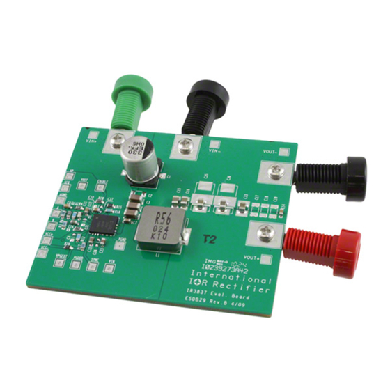
IRDC3837 SupIRBuck USER GUIDE FOR IR3837 EVALUATION BOARD DESCRIPTION Key features includes: Internal LDO, Pre-Bias The IR3837 SupIRBuck is an easy-to-use, startup, protection functions, such as hiccup fully integrated and highly efficient DC/DC current limit and thermal shutdown to give regulator. - Page 2 IRDC3837 CONNECTIONS and OPERATING INSTRUCTIONS A well regulated +12V input supply should be connected to VIN+ and VIN-. A maximum 14A load should be connected to VOUT+ and VOUT-. The connection diagram is shown in Fig. 1 and inputs and outputs of the board are listed in Table I.
- Page 3 IRDC3837 Connection Diagram GROUND Enable Vref GROUND Vcc/LDO_out PGood SYNC Fig. 1: Connection diagram of IR3838 evaluation board (top and bottom)
- Page 4 IRDC3837 Fig. 2: Board layout, top layer Fig. 3: Board layout, bottom layer...
- Page 5 IRDC3837 Single point connection between AGND and PGND. Fig. 4: Board layout, mid-layer I Fig. 5: Board layout, mid-layer II...
- Page 6 IRDC3837...
-
Page 7: Bill Of Materials
IRDC3837 Bill of Materials Item NumQuantity Part Reference Value Description Manufacturer Manufacturer Part Number 1 C1 330uF/25V SMD Elecrolytic, Fsize, 25V, 20% Panasonic EEE-FK1E331P 4 C3 C4 C5 C6 10uF Ceramic,16V,1206,X7R,20% Panasonic - ECG ECJ-3YX1C106K 5 C7 C10 C12 C14 C24 0.1uF 0603-50V-X7R-10% Panasonic... - Page 8 IRDC3837 TYPICAL OPERATING WAVEFORMS Vin=12V, Vcc/LDO=5.2V, Vo=1.8V, Io=0-14A, Room Temperature, No Air Flow Fig. 9: Start up at 14A Load (Note 1) Fig. 10: Start up at 14A Load (Note 1) :PGood Ch :EN Ch :PGood Ch :Vcc Ch Fig. 12: Output Voltage Ripple, 14A load Fig.
- Page 9 IRDC3837 TYPICAL OPERATING WAVEFORMS Vin=12V, Vcc/LDO=5.2V, Vo=1.8V, Room Temperature, No Air Flow Fig. 15: Transient Response 1.4A(10%)-5.6A(40%) load (0.5A/us) Ch , Ch Note1: Enable is tied to Vin via a resistor divider and triggered when Vin is exceeding above 10.2V. Note2: Vo ripple signal is taken across C17 cap.
- Page 10 IRDC3837 TYPICAL OPERATING WAVEFORMS Vin=12V, Vcc/LDO=5.2V, Vo=1.8V, Io=0-14A, Room Temperature, No Air Flow Fig.16: Bode Plot at 10A load shows a bandwidth of 93kHz and phase margin of 49 degrees...
- Page 11 IRDC3837 TYPICAL OPERATING WAVEFORMS Vin=12V, Vcc/LDO=5.2V, Vo=1.8V, Io=0-14A, Room Temperature, No Air Flow 10.5 11.5 12.5 13.5 14.5 Io [A] 10.5 11.5 12.5 13.5 14.5 Io [A] Fig.17: Efficiency and power loss vs. load current...
- Page 12 IRDC3837 THERMAL IMAGES Vin=12V, Vcc/LDO=5.2V, Vo=1.8V, Io=14A, Room Temperature, No Air Flow Fig.18: Thermal Image at 14A load Test Point 1: IR3837, Test Point 2: Inductor...
- Page 13 IRDC3837 PCB Metal and Components Placement The lead lands (the 13 IC pins) width should be equal to the nominal part lead width. The minimum lead to lead spacing should be ≥ 0.2mm to minimize shorting. Lead land length should be equal to the maximum part lead length + 0.3 mm outboard extension. The outboard extension ensures a large and inspectable toe fillet.
- Page 14 IRDC3837 Solder Resist It is recommended that the lead lands are Non Solder Mask Defined (NSMD). The solder resist should be pulled away from the metal lead lands by a minimum of 0.025mm to ensure NSMD pads. The land pad should be Solder Mask Defined (SMD), with a minimum overlap of the solder resist onto the copper of 0.05mm to accommodate solder resist mis-alignment.
-
Page 15: Stencil Design
IRDC3837 Stencil Design • The Stencil apertures for the lead lands should be approximately 80% of the area of the lead lads. Reducing the amount of solder deposited will minimize the occurrences of lead shorts. If too much solder is deposited on the center pad the part will float and the lead lands will be open. - Page 16 IRDC3837 MILIMITERS INCHES MILIMITERS INCHES 0.800 1.000 0.0315 0.0394 0.350 0.450 0.0138 0.0177 0.000 0.050 0.0000 0.0020 2.441 2.541 0.0961 0.1000 0.375 0.475 0.1477 0.1871 0.703 0.803 0.0277 0.0316 0.250 0.350 0.0098 0.1379 2.079 2.179 0.0819 0.0858 0.203 REF. 0.008 REF. 3.242 3.342 0.1276...
Need help?
Do you have a question about the SupIRBuck IR3837 and is the answer not in the manual?
Questions and answers