Table of Contents
Advertisement
Quick Links
UG2020-10
EVAL-FFXMR12KM1DR user guide
Evaluation board for 1200 V CoolSiC™ MOSFET 62 mm half -bridge
modules
About this document
The purpose of this board is to enable the evaluation of the FF6MR12KM1, FF3MR12KM1 and FF2MR12KM1
CoolSiC™ MOSFET modules. The evaluation board allows users to evaluate the device performance via double-
pulse measurements.
Scope and purpose
The properties of this board are described in the design features' chapter of this document. The remaining
sections provide information to enable designers to copy, modify and qualify the design for production,
according to the customer-specific requirements.
Environmental regulations have been considered in the design of the EVAL-FFXMR12KM1DR board.
Components qualified for a lead-free, reflow soldering process have been selected. The design has been tested
as described in this document, but not qualified regarding manufacturing and operation over the whole
operating temperature range or lifetime.
Intended audience
This document is intended for engineers who want to document and evaluate the switching performance of
Infineon CoolSiC™ 62 mm modules.
Evaluation board
This board will be used during design-in, for evaluation and measurement of characteristics, and proof of
datasheet specifications.
Note:
PCB and auxiliary circuits are NOT optimized for final customer design.
User Guide
Please read the Important Notice and Warnings at the end of this document
V 1.0
www.infineon.com
page 1 of 22
2020-10-20
Advertisement
Table of Contents

Related Manuals for Infineon Technologies EVAL-FFXMR12KM1DR


Summary of Contents for Infineon Technologies EVAL-FFXMR12KM1DR
-
Page 1: About This Document
Environmental regulations have been considered in the design of the EVAL-FFXMR12KM1DR board. Components qualified for a lead-free, reflow soldering process have been selected. The design has been tested as described in this document, but not qualified regarding manufacturing and operation over the whole operating temperature range or lifetime. -
Page 2: Important Notice
Boards provided by Infineon Technologies. The design of the Evaluation Boards and Reference Boards has been tested by Infineon Technologies only as described in this document. The design is not qualified in terms of safety requirements, manufacturing and operation over the entire operating temperature range or lifetime. -
Page 3: Safety Precautions
EVAL-FFXMR12KM1DR user guide Evaluation board for 1200 V CoolSiC™ MOSFET 62 mm half-bridge modules Safety precautions Safety precautions Note: Please note the following warnings regarding the hazards associated with development systems. Warning: The DC link potential of this board is up to 1000 V . -
Page 4: Table Of Contents
EVAL-FFXMR12KM1DR user guide Evaluation board for 1200 V CoolSiC™ MOSFET 62 mm half-bridge modules Table of contents Table of contents About this document ........................1 Important notice ..........................2 Safety precautions .......................... 3 Table of contents ..........................4 The board at a glance ......................5 Delivery content ............................ -
Page 5: The Board At A Glance
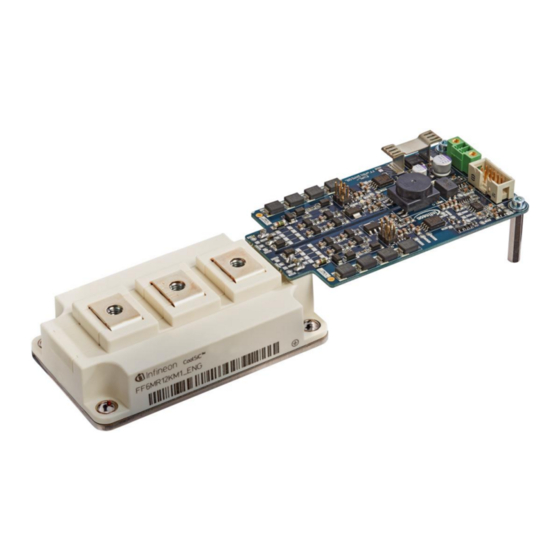
Chapter 2.2. A suitable connection of the active-clamp solder pins has to be established to use this function and make the device safe in case of an overvoltage event at turn-off. Figure 1 EVAL-FFXMR12KM1DR connected to a 62 mm CoolSiC™ Trench MOSFET moduleBlock diagram Main features Half-bridge driver for 62 mm modules with CoolSiC™... -
Page 6: Board Parameters And Technical Data
The EVAL-FFXMR12KM1DR operates with a supply voltage of up to 24 V. It generates an output voltage of up to 18 V at the gate terminals, depending on the load conditions. To switch the device, a pulse width modulation (PWM) for both, the top and the bottom side need to be applied at the connector input. -
Page 7: System And Functional Description
System and functional description Commissioning The EVAL-FFXMR12KM1DR is powered up at the phoenix-MCV, two-pin connector as shown in Figure 2. The input signals are attached by using a 10-pin, flat cable connector. Further details about the pin connector are shown in Chapter 3.4. -
Page 8: Active Voltage Clamping
Active voltage clamping Please make sure to also connect the drain sense contacts of the EVAL-FFXMR12KM1DR driver board as shown in Figure 5. This picture shows a vertical positioning of the driver board that is also possible in case other components, e.g. -
Page 9: System Design
SiC devices. Schematics The schematics that are shown here are just an excerpt from the entire documentation that can be found in the PCB design data of the EVAL-FFXMR12KM1DR board homepage at www.infineon.com. Figure 6 Positive power supply VDRV The linear voltage regulator IFX27001 in a DPAK package is used to deliver an accurate supply voltage (VDRV), which is used as supply voltage of the push-pull stage at the isolated DC-DC converter. -
Page 10: Layout
Figure 11 and Figure 12. The internal layer 1 is used for the ground signal of the secondary side and to route the signals of the driver output to the booster stage. The Gerber and ODB++ files can also be accessed via the PCB design data tab of the EVAL-FFXMR12KM1DR board homepage at www.infineon.com. FFXMR12KM1DR with the top layer highlighted... - Page 11 EVAL-FFXMR12KM1DR user guide Evaluation board for 1200 V CoolSiC™ MOSFET 62 mm half-bridge modules System design FFXMR12KM1DR with the bottom layer highlighted Figure 10 FFXMR12KM1DR with the internal layer 1 highlighted Figure 11 User guide 11 of 22 2020-10-20...
-
Page 12: Bill Of Material
Bill of material Please see the most important components of the board in Table 2. Please note that the detailed BOM of the EVAL-FFXMR12KM1DR is available at www.infineon.com. Table 2 BOM of the most important/critical parts of the evaluation or reference board (example) S. - Page 13 EVAL-FFXMR12KM1DR user guide Evaluation board for 1200 V CoolSiC™ MOSFET 62 mm half-bridge modules System design Table 4 Connector X2 Label Function X2.1 +24VIN 24 V output X2.2 Input ground X2.3 PWMTOP PWM for high side X2.4 Input ground X2.5...
-
Page 14: System Performance
EVAL-FFXMR12KM1DR user guide Evaluation board for 1200 V CoolSiC™ MOSFET 62 mm half-bridge modules System performance System performance Figure 13 captures the test setup and voltage measurement techniques for double-pulse testing. The first turn- on pulse of the low-side device (S2) establishes the desired current value (e.g. nominal data sheet current in this case) in the inductive load, and the turn-off pulse makes the current flow in the freewheeling diode (e.g. -
Page 15: Switching Performance
EVAL-FFXMR12KM1DR user guide Evaluation board for 1200 V CoolSiC™ MOSFET 62 mm half-bridge modules System performance Switching performance This chapter presents some examples of extracted waveforms of the module FF2MR12KM1, which has been characterized with the help of the evaluation board. - Page 16 EVAL-FFXMR12KM1DR user guide Evaluation board for 1200 V CoolSiC™ MOSFET 62 mm half-bridge modules System performance Turn-on losses (E ) with different gate source voltages (V = -5V … 0 V/ +15 V) and different Figure 15 driver cable lengths The influence of the length of the gate cable was observed by soldering drilled cables (8 cm/ 20 cm) onto the gate-source terminals of the board and the gate-source terminals of the module.
-
Page 17: Mosfet Switch-Off Behavior
EVAL-FFXMR12KM1DR user guide Evaluation board for 1200 V CoolSiC™ MOSFET 62 mm half-bridge modules System performance 4.1.2 MOSFET switch-off behavior The turn-off switching with different bipolar voltage levels was observed by changing the R in a way that the G,off gate current stays the same for each testing sequence. -
Page 18: Switching Behavior Of Body Diode
EVAL-FFXMR12KM1DR user guide Evaluation board for 1200 V CoolSiC™ MOSFET 62 mm half-bridge modules System performance 4.1.3 Switching behavior of body diode Although the body diode causes few losses, it is a good illustration of parasitic switch-on. Observing the switching curves during the recovery of the body diode, one can see that both the curve of the drain current as well as the drain-source voltage become very smooth. -
Page 19: Conclusion Of The Measurement Results
EVAL-FFXMR12KM1DR user guide Evaluation board for 1200 V CoolSiC™ MOSFET 62 mm half-bridge modules System performance 4.1.4 Conclusion of the measurement results: Adapted gate-source voltage (V = -5… 0 V / +15… +18 V) Turn-on losses rise slightly with higher V going from -5 V to 0 V −... -
Page 20: References And Appendices
Underwriters Laboratories References Infineon Technologies AG. AN2013-10 (Rev. 2014): External Booster for Driver IC V 1.6 www.infineon.com Infineon Technologies AG. AN2019-25: CoolSiC™ MOSFET motor drives evaluation board for 7.5 kW - Eval- M5-E1B1245N-SiC www.infineon.com Additional information The power board is now available for customers in small order quantities. -
Page 21: Revision History
EVAL-FFXMR12KM1DR user guide Evaluation board for 1200 V CoolSiC™ MOSFET 62 mm half-bridge modules Revision history Revision history Document Date of release Description of changes version 2020-10-20 Initial version User guide 21 of 22 2020-10-20... - Page 22 All referenced product or service names and trademarks are the property of their respective owners. For further information on the product, technology, Edition 2020-10-19 delivery terms and conditions and prices please contact your nearest Infineon Technologies office Published by (www.infineon.com). Infineon Technologies AG...
Need help?
Do you have a question about the EVAL-FFXMR12KM1DR and is the answer not in the manual?
Questions and answers