Table of Contents
Advertisement
Quick Links
QQ
3 7 63 1515 0
SERVICE MANUAL
Ver 1.1 2003. 05
HCD-M333 is the Amplifier, CD player, MD
deck, Tape player and Tuner section in
CMT-M333NT.
US and foreign pafents lisensed from Dolby
Labaratories.
TE
L 13942296513
Amplifier section
Canadian model:
Continuous RMS power output (reference):
Total harmonic distortion less than 0.09%
European model:
DIN power output (rated): 20 + 20 W
Continuous RMS power output (reference):
Music power output (reference):
Other models:
DIN power output:
Continuous RMS power output (reference):
www
.
Sony Corporation
9-877-180-02
Home Audio Company
2003E16-1
Published by Sony Engineering Corporation
© 2003.05
http://www.xiaoyu163.com
Inputs
ANALOG IN:
DIGITAL OPTICAL IN (supported sampling
25 + 25 W
frequencies: 32 kHz, 44.1 kHz and 48 kHz)
(6 ohms at 1 kHz, 10%
Outputs
THD)
PHONES (stereo minijack):
(6 ohms at 1 kHz, 6 W)
(6 ohms at 1 kHz, DIN)
SPEAKER:
25 + 25 W
CD player section
(6 ohms at 1 kHz, 10%
THD)
Laser
45 + 45 W
20 + 20 W
Frequency response
(6 ohms at 1 kHz, DIN)
25 + 25 W
(6 ohms at 1 kHz, 10%
THD)
x
ao
u163
y
i
http://www.xiaoyu163.com
HCD-M333
2 9
8
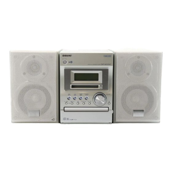
Photo : SILVER TYPE
Model Name Using Similar Mechanism
CD
CD Mechanism Type
Section
Base Unit Type
Optical Pick-up Type
Model Name Using Similar Mechanism
MD
Q Q
MD Mechanism Type
3
6 7
1 3
1 5
Section
Optical Pick-up Type
Tape deck
Model Name Using Similar Mechanism
Section
Tape Transport Mechanism Type
SPECIFICATIONS
Sensitivity 250 mV,
impedance 47 kilohms
accepts headphones with
an impedance of 8 ohms or
more
accepts impedance of 6 to
16 ohms
Semiconductor laser
(CD: λ=780 nm)
Emission duration:
continuous
2 Hz – 20 kHz
MICRO HI-FI COMPONENT SYSTEM
co
.
9 4
2 8
Canadian Model
AEP Model
UK Model
E Model
Chinese Model
Australian Model
NEW
CDM55A-30BBD61B
BU-30BBD61B
A-MAX. 3
HCD-CP505
MDM-7S2D
0 5
8
2 9
9 4
2 8
KMS-262E
NEW
CMAL1Z-236A
MD deck section
System
Minidisc digital audio
system
Laser
Semiconductor laser
(λ=780 nm)
Emission duration:
continuous
Sampling frequency
44.1 kHz
Frequency response
5 Hz – 20 kHz
Tape deck section
Recording system
4-track 2-channel stereo
Frequency response
60 – 10,000 Hz (±3 dB),
using Sony TYPE I
cassettes
— Continued on next page —
m
9 9
9 9
Advertisement
Table of Contents

Related Manuals for Sony HCD-M333


Summary of Contents for Sony HCD-M333
- Page 1 Ver 1.1 2003. 05 UK Model E Model Chinese Model Australian Model HCD-M333 is the Amplifier, CD player, MD deck, Tape player and Tuner section in CMT-M333NT. Photo : SILVER TYPE US and foreign pafents lisensed from Dolby Model Name Using Similar Mechanism Labaratories.
- Page 2 HCD-M333 Ver 1.1 2003.05 3 7 63 1515 0 Tuner section Other models: 530 – 1,710 kHz Dimensions (w/h/d) incl. projecting parts and controls (with the tuning interval Amplifier/Tuner/Tape/MD/CD section: FM stereo, FM/AM superheterodyne tuner set at 10 kHz) Approx.
-
Page 3: Table Of Contents
CRITIQUES POUR LA SÉCURITÉ DE FONCTIONNEMENT. NE REMPLACER CES COMPOSANTS QUE PAR DES PIÈSES SONY as on IC pins, etc. DONT LES NUMÉROS SONT DONNÉS DANS CE MANUEL OU •... - Page 4 No component is connected to the DIGITAL refer to the following list. If any problem OPTICAL IN jack, or you tried to record from the persists, consult your nearest Sony dealer. digital component which is not connected correctly. c Connect the optional digital component correctly to the DIGITAL OPTICAL IN jack using the digital optical cable (not supplied) (page 52).
- Page 5 HCD-M333 3 7 63 1515 0 Group Full! Messages An attempt was made to create a new group in excess of the maximum number of groups, or there One of the following messages may appear or are insufficient characters for updating the group flash in the display during operation.
- Page 6 HCD-M333 3 7 63 1515 0 S.F Edit NOW Optional personal computer You pressed ?/ 1 while in S.F Edit (changing the Buffer recording level after recording, Fade-in, Fade-out) The personal computer is preparing the amount of mode. data needed for playback while using the WEB Smart Space RADIO function.
-
Page 7: Qq
HCD-M333 3 7 63 1515 0 Note 1: About “R” As this unit has only a few buttons, some operations require the use of remote commander (RM-SM100W/provided with unit) buttons. These operations are indicated as “R” in this manual. - Page 8 HCD-M333 3 7 63 1515 0 Items of Error History Mode Items and Contents Display History op rec tm Displays the accumulated recording time. When the accumulated recording time is more than 1 minute, displays the hour and minute When less than 1 minute, displays “Under 1 min”...
- Page 9 HCD-M333 3 7 63 1515 0 Table of Error Codes Error Code Description Could not perform loading The changer error occurred Loading switches combined incorrectly Timed out without reading the top of PTOC Could read top of PTOC, but detected error...
-
Page 10: Servicing Notes
HCD-M333 SECTION 1 SERVICING NOTE 3 7 63 1515 0 Note 1: About “R” As this unit has only a few buttons, some operations require the use of remote commander (RM-SM100W/provided with unit) buttons. These operations are indicated as “R” in this manual. - Page 11 HCD-M333 3 7 63 1515 0 Service Position-2 (Checking CD Mechanism and MD Mechanism Section) MAIN BOARD MD DIGITAL BOARD MD mechanism deck section CD mechanism deck section (MDM-7S2D) (CDM55A-30BBD6) L 13942296513 Service Position-3 (Checking Power Supply Section) Connect the POWER board (CN985) and the AMP board (CN805) with the extension cable (6P)(J-2501-229-A).
- Page 12 HCD-M333 3 7 63 1515 0 Jig For Checking BD (MD) Board Waveform The special jig (J-2501-196-A) is useful for checking the waveform of the BD (MD) board. The names of terminals and the checking items to be performed are shown as follows.
- Page 13 HCD-M333 3 7 63 1515 0 Iop DATA RECORDING AND DISPLAY WHEN OPTICAL PICK-UP AND NON-VOLATILE MEMORY (IC195 OF BD (MD) BOARD) ARE REPLACED The Iop value labeled on the optical pick-up can be stored in the non-volatile memory. By storing the value, it will eliminate the need to look at the value on the label of the optical pick-up.
-
Page 14: General
HCD-M333 SECTION 2 This section is extracted GENERAL 3 7 63 1515 0 from instruction manual. Main unit BUTTON DESCRIPTIONS ALPHABETICAL ORDER ?/1 (power) 1 (6, 15, 23, 37, 43, M – Z A – L MD slot 6... - Page 15 HCD-M333 3 7 63 1515 0 Remote control ALPHABETICAL ORDER BUTTON DESCRIPTIONS ?/1 (power) 1 (6, 15, 23, 43) A – L M – Z +/– 5 (36, 37) BASS/TRE 9 (42) MENU/NO wh (10, 19, 20, 21, 23, ./>...
-
Page 16: Disassembly
HCD-M333 SECTION 3 DISASSEMBLY 3 7 63 1515 0 • The equipment can be removed using the following procedure. TOP PANEL SECTION FRONT PANEL SECTION CASSETTE MECHANISM DECK PANEL BOARD, H/P BOARD, BACK PANEL SECTION LED BOARD MAIN BOARD... -
Page 17: Top Panel Section
HCD-M333 3 7 63 1515 0 Note: Follow the disassembly procedure in the numerical order given. 3-1. Top Panel Section qa case (T) (Remove the direction of the arrow. 3 screw (BVTP 3 × 10) qf cover (B/P) 1 two screws (case 3 TP2) -
Page 18: Cassette Mechanism Deck
HCD-M333 3 7 63 1515 0 3-2. Cassette Mechanism Deck qf lid (TC) assy case (T) qs torsion spring (tc) 7 two screws (BVTT 2.6 × 5) 9 tape mechanism deck 8 shield (tc2) 5 two screws (BVTP 3 × 8) 6 two screws (BVTP 3 ×... -
Page 19: Panel Board, H/P Board, Led Board
HCD-M333 3 7 63 1515 0 3-4. PANEL Board, H/P Board, LED Board front panel assy 1 knob spin (vol) L 13942296513 front panel qa screw (PTPWH M2.6 × 8) qs lid (MD) qd torsion spring (lid MD) 2 two screws (BVTP 2.6 ×... -
Page 20: Back Panel Section
HCD-M333 3 7 63 1515 0 3-5. Back Panel Section 6 two screws (B 4 × 12) 1 connector (CN803) 2 screw (BVTT 3 × 6) 7 two nuts (N4) 3 four screws (BVTP 3 × 8) 4 three screws (BVTP 3 × 8) -
Page 21: Md Mechanism Deck (Mdm-7S2D)
HCD-M333 3 7 63 1515 0 3-7. MD Mechanism Deck (MDM-7S2D) 1 two screws (BVTP 3 × 6) 3 flat type wire (17 core) (CN703) 2 shield MD (U) 4 flat type wire (27 core) (CN702) 7 two step screws... -
Page 22: Holder Assy
HCD-M333 3 7 63 1515 0 3-9. Holder Assy 3 holder assy 1 tension spring (holder) 2 hook L 13942296513 3-10. BD (MD) Board 1 Remove the two solderings (sled motor) 2 Remove the two solderings (spindle motor) M102... -
Page 23: Motor Section
HCD-M333 3 7 63 1515 0 3-11. Motor Section 1 lever (head) 8 tapping screw 3 torsion spring (spindle) (M1.7 ) 2 belt (loading) 9 gear (sa) 4 two screws 0 two screws (PWH 1.7 × 3.5) (PWH 1.7 × 2.5) -
Page 24: Mini Disc Device (Kms-262E)
HCD-M333 3 7 63 1515 0 3-13. Mini Disc Device (KMS-262E) 8 Mini disc device (KMS-262E) 6 main shaft 3 screw (+B (P) TRI 2 × 6 CZN) 4 base (BU-A) 7 flexible board 5 two screws (+KTP 2 × 6) 1 screw (+B (P) TRI 2 ×... -
Page 25: Reg Board, Amp Board
HCD-M333 3 7 63 1515 0 3-15. REG Board, AMP Board 3 screw (BVTT 3 × 6) heat sink 6 REG board flat type wire (11 core) (CN106) 5 screw (BVTT 3 × 6) qa AMP board 4 four screws (BVTP 2.6 × 8) 7 screw (BVTP 3 ×... -
Page 26: Cd Mechanism Deck (Cdm55A-30Bbd61B)
HCD-M333 3 7 63 1515 0 3-17. CD Mechanism Deck (CDM55A-30BBD61B) 1 screw (BVTT 3 × 6) 3 loading panel asy 4 CD mechanism deck (CDM55A-30BBD61B) L 13942296513 3-18. Cam (CDM55) 4 belt (CDM55) 5 spacer (55) 6 pulley (LDG) -
Page 27: Base Unit (Bu-30Bbd61B)
HCD-M333 3 7 63 1515 0 3-19. Base Unit (BU-30BBD61B) 2 Remove the base unit (BU-30BBD61B) 1 floating screw in the direction of the arrow A . (+PTPWH M2.6) 3 chassis (55D) 3-20. Optical Pick Up (BU-30B Assy) L 13942296513... -
Page 28: Test Mode
HCD-M333 SECTION 4 TEST MODE 3 7 63 1515 0 Note 1: About “R” As this unit has only a few buttons, some operations require the use of remote commander (RM-SM100W/provided with unit) buttons. These operations are indicated as “R” in this manual. - Page 29 HCD-M333 3 7 63 1515 0 4. CD Ship Mode (Setting the Position for Transportation) Press the ?/1 button to turn the power on. Press the FUNCTION to change the function to “CD”. Press two buttons x , ENTER/START and press the CD u button simultaneously.
- Page 30 HCD-M333 3 7 63 1515 0 MD TEST MODE 1. Precautions For Use of Test Mode • As operations related to loading will be performed regardless of the test mode operations being performed, be sure to check that the disc is stopped before setting and removing it.
- Page 31 HCD-M333 3 7 63 1515 0 Group Display Details Mark Check Service AUTO CHECK Automatic self-diagnosis Err Display Error history display, clear TEMP ADJUST Temperature compensation offset adjustment LDPWR ADJUST Laser power adjustment Iop Write Iop data writing Iop NV Save...
- Page 32 HCD-M333 3 7 63 1515 0 5-2. Operating the Continuous Recording Mode (Use only when performing self-recording/playback check) Entering the continuous recording mode (1) Set a recordable disc in the unit. (2) Press the . “R” or > “R” button to display “CRE 2MODE”...
-
Page 33: Electrical Adjustments
HCD-M333 SECTION 5 ELECTRICAL ADJUSTMENTS 3 7 63 1515 0 Mode: Playback TAPE SECTION 0 dB=0.775V Demagnetize the record/playback head with a head demagne- test tape tizer. P-4-A100 MAIN board (10kHz, –10dB) Do not use a magnetized screwdriver for the adjustments. - Page 34 HCD-M333 3 7 63 1515 0 Record Bias Adjustment Record Level Adjustment Procedure : Procedure : 1. Press the FUNCTION button to select ANALOG IN. 1. Press the FUNCTION button to select ANALOG IN. 2. Insert a tape into deck, press the z TAPE button, and then 2.
-
Page 35: Cd Section
HCD-M333 3 7 63 1515 0 E-F Balance (1 Track jump) Check CD SECTION Note : Oscilloscope 1. CD Block is basically designed to operate without adjustment. BD (CD) BOARD Therefore, check each item in order given. 2. Use YEDS-18 disc (3-702-101-01) unless otherwise indicated. -
Page 36: Md Section
HCD-M333 3 7 63 1515 0 MD SECTION Note 1: About “R” As this unit has only a few buttons, some operations require the use of remote commander (RM-SM100W/provided with unit) buttons. These operations are indicated as “R” in this manual. - Page 37 HCD-M333 3 7 63 1515 0 Flow Chart for Adjustment Start After turning the power off and on, initialises the non-volatile IC195 replacement memory (EEPROM). 7. Initial setting of adjustment value (See page 42) OP or IC195 replacement IC101, IC195 or D101 9.
- Page 38 HCD-M333 3 7 63 1515 0 Precautions for Checking Laser Diode 5. When observing several signals on the oscilloscope, etc., make sure that VC and ground do not connect inside the Emission oscilloscope. To check the emission of the laser diode during adjustments, never (VC and ground will become short-circuited.)
- Page 39 HCD-M333 3 7 63 1515 0 Using the Continuously Recorded Disc Procedure: Set the laser power meter on the objective lens of the optical * This disc is used in focus bias adjustment and error rate check. pick-up. (When it cannot be set properly, press the m but- The following describes how to create a continuous recording ton or M button to move the optical pick-up.)
- Page 40 HCD-M333 3 7 63 1515 0 6-4. Auto Check 6-6. Traverse Check This test mode performs CREC and CPLAY automatically for mainly checking the characteristics of the optical pick-up. To Note 1:Data will be erased during MO reading if a recorded disc is used in this adjustment.
- Page 41 HCD-M333 3 7 63 1515 0 6-7. Focus Bias Check 9. Press the ENTER/YES “R” button to display “EFB = Change the focus bias and check the focus tolerance amount. MO-P”. Procedure: Then, the optical pick-up moves to the pit area automatically 1.
- Page 42 HCD-M333 3 7 63 1515 0 Initial Setting of Adjustment Value 5. When the ENTER/YES “R” button is pressed, “TEMP = Note: SAVE” will be displayed and turned back to “TEMP ADJUST” Mode which sets the adjustment results recorded in the non-volatile (C03) display then.
- Page 43 HCD-M333 3 7 63 1515 0 6. Press the “R” or > “R” button so that the reading of After the display changes to “Iop = save?”, press the laser power meter becomes the specified value, press the ENTER/YES “R” button.
- Page 44 HCD-M333 3 7 63 1515 0 19. Press the Z (MD) button and take out the check disc. 8. Press the “R” or > “R” button so that the waveform of the oscilloscope becomes the specified value. Adjustment Location: BD (MD) board (see page 46) (When the “R”...
- Page 45 HCD-M333 3 7 63 1515 0 14. Error Rate Check 16. Auto Gain Control Output Level Adjustment Be sure to perform this adjustment when the optical pick-up is 14-1. CD Error Rate Check replaced. Procedure: If the adjustment results becomes “Adjust NG!”, the optical pick- 1.
- Page 46 HCD-M333 3 7 63 1515 0 Adjustment and checking Loacation: — BD (MD) BOARD (Side A) — — BD (MD) BOARD (Side A) — CN102 CN103 IC195 IC933 IC201 IC701 CN101 CN105 IC101 D101 Note: If is useful to use the jig for checking the waveform.
-
Page 47: Diagrams
HCD-M333 Ver 1.1 2003.05 SECTION 6 3 7 6 3 1 5 1 5 0 DIAGRAMS 6-1. Circuit Boards Location • Waveforms REG BOARD POWER BOARD BD (CD) Board BD (MD) Board AMP BOARD T/C BOARD MD DIGITAL BOARD... -
Page 48: Block Diagrams
HCD-M333 6-2. Block Diagrams 3 7 6 3 1 5 1 5 0 IC104 – CD Section – SELECTOR OPTICAL PICK-UP BLOCK IC103 IC101 (A-MAX.3) RF AMP DIGITAL SERVO DIGITAL SIGNAL PROC. IC105 DIN-CD DOUT SECTION IC101 (1/2) RFAC... -
Page 49: Md Section
HCD-M333 – – MD Section 3 7 6 3 1 5 1 5 0 IC201 DIGITAL SERVO DIGITAL SIGNAL PROC. DATAI IC181 DATAI Q181,182 LRCKI HR901 LRCKI XBCKI OVER WRITE OVER WRITE EFMO XBCKI HEAD DRIVE HEAD MCLK FS256... -
Page 50: Usb Section
HCD-M333 – – USB Section 3 7 6 3 1 5 1 5 0 IC701 AD/DA CONVERTER IC253 IC252 BUFFER DIGITAL DIGITAL DIN-OPT OPTICAL OPTICAL 2 RX3 42 RX1 LOUT MAIN LOUT DIN-CD SECTION 44 RX2 ROUT R-CH SECTION... -
Page 51: Main Section
HCD-M333 – – MAIN Section 3 7 6 3 1 5 1 5 0 R-CH J401 PHONES SECTION IC803 IC102 SOUND PROCESSOR POWER AMP LOUT SJ302 SECTION L OUT OUT+ ANALOG Q874 Q801 L SEL O 10 STBY TM801... -
Page 52: Printed Wiring Board - Bd (Cd) Board
HCD-M333 6-3. Printed Wiring Board – BD (CD) Board – • See page 47 for Circuit Boards Location. • : Uses unleaded solder. 3 7 6 3 1 5 1 5 0 M902 (A-MAX.3) IC201 IC103 IC101 MAIN BOARD... -
Page 53: Schematic Diagram - Bd (Cd) Board
HCD-M333 6-4. Schematic Diagram – BD (CD) Board – • See page 76-77 for IC Block Diagrams. • See page 47 for Waveforms. 3 7 6 3 1 5 1 5 0 TP39 TP49 C253 IC104 TC74HC4052 AFT(EL) (RFAC) -
Page 54: Printed Wiring Board - Bd (Md) Board
HCD-M333 6-5. Printed Wiring Board – BD (MD) Board – • See page 47 for Circuit Boards Location. • : Uses unleaded solder. 3 7 6 3 1 5 1 5 0 (Page 57) (Page 57) IC181 IC803 IC933... -
Page 55: Schematic Diagram - Bd (Md) Board (1/2)
HCD-M333 6-6. Schematic Diagram – BD (MD) Board (1/2) – • See page 78,80 for IC Block Diagrams. • See page 47 for Waveforms. 3 7 6 3 1 5 1 5 0 1 3 9 4 2 2 9 6 5 1 3... -
Page 56: Schematic Diagram - Bd (Md) Board (2/2)
HCD-M333 6-7. Schematic Diagram – BD (MD) Board (2/2) – • See page 79 for IC Block Diagrams. • See page 47 for Waveforms. 3 7 6 3 1 5 1 5 0 (MD) (2/2) S105 (REC) TP935 S104... -
Page 57: Printed Wiring Board - Md Digital Board
HCD-M333 Ver 1.1 2003.05 6-8. Printed Wiring Board – MD DIGITAL Board – • See page 47 for Circuit Boards Location. 3 7 6 3 1 5 1 5 0 R726 • Semiconductor Location IC704 Ref. No. Location D751... -
Page 58: Schematic Diagram - Md Digital Board (1/2)
HCD-M333 Ver 1.1 2003.05 6-9. Schematic Diagram – MD DIGITAL Board (1/2) – • See page 81-83 for IC Block Diagrams. • See page 87 for IC Pin Function Descriptions. • See page 47 for Waveforms. 3 7 6 3 1 5 1 5 0... -
Page 59: Schematic Diagram - Md Digital Board (2/2)
HCD-M333 6-10. Schematic Diagram – MD DIGITAL Board (2/2) – • See page 81,83 for IC Block Diagrams. • See page 87,89 for IC Pin Function Descriptions. • See page 47 for Waveforms. 3 7 6 3 1 5 1 5 0... -
Page 60: Printed Wiring Board - Tc Board
HCD-M333 6-11. Printed Wiring Board – TC Board – • See page 47 for Circuit Boards Location. • : Uses unleaded solder. 3 7 6 3 1 5 1 5 0 (Page 62) • Semiconductor Location 1 3 9 4 2 2 9 6 5 1 3 Ref. -
Page 61: Schematic Diagram - Tc Board
HCD-M333 6-12. Schematic Diagram – TC Board – • See page 47 for Waveforms. 3 7 6 3 1 5 1 5 0 CN602 Q694 2SB1068 IC602 BA3126N R695 R694 R693 R683 R687 R688 4.7k C607 Q693 470p 50V B... -
Page 62: Printed Wiring Board - Main Section
HCD-M333 Ver 1.1 2003.05 6-13. Printed Wiring Board – MAIN Section – • See page 47 for Circuit Boards Location. • : Uses unleaded solder. 3 7 6 3 1 5 1 5 0 (Page 60) (Page 52) (Page 71) -
Page 63: Schematic Diagram - Main Section (1/2)
HCD-M333 6-14. Schematic Diagram – MAIN Section (1/2) – • See page 84 for IC Block Diagrams. 3 7 6 3 1 5 1 5 0 CN220 (Page 61) (Page 72) C348 CN106 CN301 100p CN105 C302 C347 100p... -
Page 64: Schematic Diagram - Main Section (2/2)
HCD-M333 Ver 1.1 2003.05 6-15. Schematic Diagram – MAIN Section (2/2) – • See page 84 for IC Block Diagrams. • See page 85 for IC Pin Function Descriptions. • See page 47 for Waveforms. 3 7 6 3 1 5 1 5 0... -
Page 65: Printed Wiring Board - H/P Board
HCD-M333 6-16. Printed Wiring Board – H/P Board – • See page 47 for Circuit Boards Location. • : Uses unleaded solder. 3 7 6 3 1 5 1 5 0 C493 1 3 9 4 2 2 9 6 5 1 3... -
Page 66: Schematic Diagram - H/P Board
HCD-M333 6-17. Schematic Diagram – H/P Board – 3 7 6 3 1 5 1 5 0 R425 R426 R427 C422 0.01 S427 S428 1 3 9 4 2 2 9 6 5 1 3 WIR404 R432 R433 R431... -
Page 67: Printed Wiring Board - Panel Section
HCD-M333 Ver 1.1 2003.05 6-18. Printed Wiring Board – PANEL Section – • See page 47 for Circuit Boards Location. • : Uses unleaded solder. 3 7 6 3 1 5 1 5 0 (Page 62) (LCD BACKLIGHT) (EXCEPT HK... -
Page 68: Schematic Diagram - Panel Section
HCD-M333 Ver 1.1 2003.05 6-19. Schematic Diagram – PANEL Section – 3 7 6 3 1 5 1 5 0 LCD401 TP408 TP407 TP406 TP405 TP401 TP402 R467 R469 C464 C465 0.01 0.001 D466 SELU5920C-TP15 D465 SELU5920C-TP15 R405 R468... -
Page 69: Reg Board / Trans Board
HCD-M333 6-20. Printed Wiring Board – REG Board / TRANS Board – • See page 47 for Circuit Boards Location. • : Uses unleaded solder. 3 7 6 3 1 5 1 5 0 POWER TRANSFORMER (MAIN) (Page73) (Page 73) -
Page 70: Schematic Diagram - Reg Board / Trans Board
HCD-M333 Ver 1.1 2003.05 6-21. Schematic Diagram – REG Board / TRANS Board – 3 7 6 3 1 5 1 5 0 T901 WIR993 C903 IC903 TA7808S CN991 C994 JW991 0.01 T992 250V BLUE BROWN WIR901 C904 JW992... -
Page 71: Printed Wiring Board - Amp Board
HCD-M333 6-22. Printed Wiring Board – AMP Board – • See page 47 for Circuit Boards Location. • : Uses unleaded solder. 3 7 6 3 1 5 1 5 0 SPEAKER • Semiconductor Location Ref. No. Location D801... -
Page 72: Schematic Diagram - Amp Board
HCD-M333 6-23. Schematic Diagram – AMP Board – 3 7 6 3 1 5 1 5 0 D831 1SS355 R833 Q832 4.7k 2SC2412 1/4W Q834 R836 2SC2412 C833 1/10W R843 R839 R840 100k Q837 R842 1/10W 1/10W 2SC2412 1/10W... -
Page 73: Printed Wiring Board - Power Board
HCD-M333 6-24. Printed Wiring Board – POWER Board – • See page 47 for Circuit Boards Location. • : Uses unleaded solder. 3 7 6 3 1 5 1 5 0 (Page 69) (Page 71) (Page 62) • Semiconductor Location Ref. -
Page 74: Schematic Diagram - Power Board
HCD-M333 Ver 1.1 2003.05 6-25. Schematic Diagram – POWER Board – 3 7 6 3 1 5 1 5 0 D983 D3SBA20 CN985 CN984 C985 F987 C986 F985 (Page 72) IC911 TA7810S (Page 70) CN981 C912 C911 JW911 C909 0.001... -
Page 75: Ic Block Diagrams
HCD-M333 3 7 63 1515 0 6-26. IC Block Diagrams – BD (CD) Board – IC101 CXD3068Q L 13942296513 u163 http://www.xiaoyu163.com... - Page 76 HCD-M333 3 7 63 1515 0 – BD (MD) Board – IC102 AN41050 CHARGE PUMP1 LOGIC BRIDGE DRIVER LOGIC BRIDGE DRIVER LOGIC BRIDGE DRIVER LOGIC BRIDGE DRIVER SAWTOOTH GEN CHARGE STANDBY PUMP2 L 13942296513 1 2 3 4 5 6 7 8 9...
- Page 77 HCD-M333 3 7 63 1515 0 IC103 CXA2581N-T4 L 13942296513 IC104 TC74HC4052AFT(EL) u163 http://www.xiaoyu163.com...
- Page 78 HCD-M333 3 7 63 1515 0 – BD (MD) Board – IC101 CXA2523AR 43 42 38 37 USROP – RF AGC – USRC RFA1 BPF3T RFA2 RFA3 PEAK3T – HLPT –1 – – –2 – OFST WBL TEMP PTGR PEAK –...
- Page 79 HCD-M333 3 7 63 1515 0 IC201 CXD2664R 114 113 112 110 109 108 107 106 105 104 103 102 101 100 99 98 97 93 92 DCHG AVS2 AVD2 SPINDLE GENERATOR SERVO MNT0 (FOK) 85 SE MNT1 (SHCK)
- Page 80 HCD-M333 3 7 63 1515 0 IC401 BH6519FS-E2 INTERFACE INTERFACE CHARGE PREDRIVE PREDRIVE PUMP. PREDRIVE PREDRIVE INTERFACE INTERFACE IC803 CY24115-2SCT L 13942296513 XOUT ‡ OUTPUT DIVIDERS CLKSEL FREQUENCY TABLE CLKA u163 http://www.xiaoyu163.com...
- Page 81 HCD-M333 3 7 63 1515 0 – MD DIGITAL Board – IC701 AK4584VQ TEST2 33 ROUT LOUT A_LRCK D_LRCK A_BICK D_BICK DATT DATT IPGA A_DATA D_DATA VCOM SMUTE A_MCLK D_MCLK S_LRCK AUDIO S_BICK INTERFACE S_DATAI 29 M/S S_DATAO R_LRCK...
- Page 82 HCD-M333 3 7 63 1515 0 IC706 PCM2903EG/2K LOCK POWER S/PDIF DECODER MANAGER VINL ISO-IN FIFO END-POINT VINR ANALOG CONTROL VCOM SELECTOR D– END-POINT ANALOG VOUTL ISO-OUT FIFO SEL0 END-POINT VOUTR SEL1 HID0 HID1 END-POINT HID2 S/PDIF ENCODER PROTOCOL...
- Page 83 HCD-M333 3 7 63 1515 0 – MAIN Board – IC102 LC75342 CONTROL LOGIC IC220 BA6956AN CONTROL LOGIC L 13942296513 u163 http://www.xiaoyu163.com...
-
Page 84: Ic Pin Function Description
HCD-M333 3 7 63 1515 0 6-27. IC PIN FUNCTION DESCRIPTION • IC101 M30622MGN-B16FP SYSTEM CONTROL (MAIN Board) Pin No. Pin Name Description LCD ON LCD display power supply control signal output ST-RDS-DATA RDS data input (AEP, UK) LCD-RST... - Page 85 HCD-M333 3 7 63 1515 0 Pin No. Pin Name Description LED-LCD-BL Back light control signal output VOL-B Volume signal input from the rotary encoder VOL-A Volume signal input from the rotary encoder CD-LDON LDON signal output to the RF amplifier (IC103)
- Page 86 HCD-M333 3 7 63 1515 0 • IC702 M30823MH-A07GP MASTER CONTROLLER (MD DIGITAL Board) Pin No. Pin Name Description A-IN — Not used (open) RMC/LEVEL-R — Not used (open) NETMD-SO Serial communication data output to the USB Net MD IC (IC705)
- Page 87 HCD-M333 3 7 63 1515 0 Pin No. Pin Name Description XLAT Latch signal output to the DSP (IC201) Serial communication clock output to the EEPROM OUT-SW Detection signal inut from the loading position switch (OUT SW) MNT2 Busy monitor signal input from the mechanism deck...
- Page 88 HCD-M333 3 7 63 1515 0 • IC703 MB89595CPFV-G-127-BND USB I/F (MD DIGITAL Board) Pin No. Pin Name Description Clock input from the USB I2C converter (IC704) Serial data output to the USB I2C converter (IC704) Serial data input from the USB I2C converter (IC704)
- Page 89 HCD-M333 3 7 63 1515 0 • IC704 MB89537ACPFM-G-405-BND USB-I2C CONVERTER (MD DIGITAL Board) Pin No. Pin Name Description 1 to 10 — Not used (open) AVCC — Power supply terminal (A/D converter) — Reference voltage terminal (A/D converter) AVSS —...
-
Page 90: Exploded Views
HCD-M333 Ver 1.1 2003.05 SECTION 7 EXPLODED VIEWS 3 7 63 1515 0 NOTE: • -XX, -X mean standardized parts, so they may • Abbreviation The components identified by mark 0 or dotted line with mark 0 are critical for safety. -
Page 91: Front Panel Section
Part No. Description Remarks Ref. No. Part No. Description Remarks 4-925-161-81 EMBLEM (4-A), SONY (EXCEPT HK,KR) 4-243-223-13 BUTTON (PLAY)(SILVER)(HK,KR) 4-925-161-91 EMBLEM (4-A), SONY (HK,KR) 4-243-198-01 PLATE, LIGHT GUIDE 4-246-117-01 KNOB SPIN (VOL) 4-243-208-01 BUTTON (MD EJECT) 4-243-197-03 LID (REC)(WHITE)(HK) (EXCEPT (SILVER)(HK,KR)) -
Page 92: Back Panel Section
HCD-M333 Ver 1.1 2003.05 3 7 63 1515 0 7-3. Back Panel Section supplied F983 F981 F987 F985 supplied supplied T900 supplied L 13942296513 not supplied not supplied CD mechanism deck section (CDM55A-30BBD61B) Ref. No. Part No. Description Remarks Ref. -
Page 93: Md Mechanism Deck Section-1 (Mdm-7S2D)
HCD-M333 3 7 63 1515 0 7-4. MD Mechanism Deck Section-1 (MDM-7S2D) supplied supplied not supplied L 13942296513 MD mechanism deck section-2 (MDM-7S2D) Ref. No. Part No. Description Remarks Ref. No. Part No. Description Remarks * 151 4-996-267-01 BASE (BU-D) -
Page 94: Md Mechanism Deck Section-2 (Mdm-7S2D)
HCD-M333 Ver 1.1 2003.05 3 7 63 1515 0 7-5. MD Mechanism Deck Section-2 (MDM-7S2D) HR901 S102 M101 L 13942296513 M102 M103 Ref. No. Part No. Description Remarks Ref. No. Part No. Description Remarks 4-231-319-01 SCREW (2X6) CZN, +B (P) TRI... -
Page 95: Cd Mechanism Deck Section-1
HCD-M333 3 7 63 1515 0 7-6. CD Mechanism Deck Section-1 (CDM55A-30BBD61B) supplied M201 L 13942296513 CD mechanism deck section-2 (BU-30BBD61B) Ref. No. Part No. Description Remarks Ref. No. Part No. Description Remarks 4-925-315-31 DAMPER 4-220-234-01 PULLEY (LDG) 4-224-894-22 TRAY (CDM55D) -
Page 96: Cd Mechanism Deck Section-2 (Bu-30Bbd61B)
HCD-M333 Ver 1.1 2003.05 3 7 63 1515 0 7-7. CD Mechanism Deck Section-2 (BU-30BBD61B) not supplied supplied supplied with 311 supplied supplied M901 L 13942296513 Ref. No. Part No. Description Remarks Ref. No. Part No. Description Remarks 4-229-358-01 SHAFT (BU21) -
Page 97: Electrical Parts List
HCD-M333 Ver 1.1 2003.05 SECTION 8 ELECTRICAL PARTS LIST 3 7 63 1515 0 NOTE: • Due to standardization, replacements in the • RESISTORS • Abbreviation parts list may be different from the parts All resistors are in ohms. - Page 98 HCD-M333 Ver 1.1 2003.05 BD (CD) 3 7 63 1515 0 Ref. No. Part No. Description Remarks Ref. No. Part No. Description Remarks Q837 8-729-120-28 TRANSISTOR 2SC2412K-T-146-QR 0 R850 1-202-972-61 FUSIBLE 1/4W Q841 8-729-120-28 TRANSISTOR 2SC2412K-T-146-QR Q842 8-729-120-28 TRANSISTOR...
- Page 99 HCD-M333 BD (CD) 3 7 63 1515 0 Ref. No. Part No. Description Remarks Ref. No. Part No. Description Remarks C113 1-126-209-11 ELECT CHIP 100uF 20.00% 4V < FERRITE BEAD > C114 1-162-964-11 CERAMIC CHIP 0.001uF C115 1-126-205-11 ELECT CHIP 47uF 6.3V...
- Page 100 HCD-M333 BD (CD) BD (MD) 3 7 63 1515 0 Ref. No. Part No. Description Remarks Ref. No. Part No. Description Remarks R209 1-216-809-11 METAL CHIP 1/16W C211 1-162-927-11 CERAMIC CHIP 100PF R212 1-216-809-11 METAL CHIP 1/16W C212 1-162-927-11 CERAMIC CHIP...
- Page 101 HCD-M333 BD (MD) 3 7 63 1515 0 Ref. No. Part No. Description Remarks Ref. No. Part No. Description Remarks C1102 1-115-416-11 CERAMIC CHIP 0.001uF 5.00% 25V R102 1-219-724-11 METAL CHIP 1/4W R103 1-216-829-11 METAL CHIP 4.7K 1/16W < CONNECTOR >...
- Page 102 HCD-M333 Ver 1.1 2003.05 BD (MD) DIGITAL 3 7 63 1515 0 Ref. No. Part No. Description Remarks Ref. No. Part No. Description Remarks R709 1-218-855-11 METAL CHIP 2.2K 0.5% 1/10W C739 1-162-970-11 CERAMIC CHIP 0.01uF C740 1-162-974-11 CERAMIC CHIP 0.01uF...
- Page 103 HCD-M333 Ver 1.1 2003.05 DIGITAL 3 7 63 1515 0 Ref. No. Part No. Description Remarks Ref. No. Part No. Description Remarks FB704 1-500-445-21 FERRITE R717 1-216-864-11 METAL CHIP 1/16W FB705 1-500-445-21 FERRITE R718 1-216-864-11 METAL CHIP 1/16W FB706...
- Page 104 HCD-M333 Ver 1.1 2003.05 DIGITAL LOADING MAIN 3 7 63 1515 0 Ref. No. Part No. Description Remarks Ref. No. Part No. Description Remarks R790 1-216-864-11 METAL CHIP 1/16W C465 1-163-009-91 CERAMIC CHIP 0.001uF 10.00% 50V R791 1-216-823-11 METAL CHIP 1.5K...
- Page 105 HCD-M333 Ver 1.1 2003.05 MAIN 3 7 63 1515 0 Ref. No. Part No. Description Remarks Ref. No. Part No. Description Remarks C233 1-107-826-11 CERAMIC CHIP 0.1uF 10.00% 16V C303 1-162-964-11 CERAMIC CHIP 0.001uF C304 1-125-972-91 ELECT 100uF 20.00% 16V...
- Page 106 HCD-M333 Ver 1.1 2003.05 MAIN 3 7 63 1515 0 Ref. No. Ref. No. Part No. Part No. Description Description Remarks Remarks Ref. No. Ref. No. Part No. Part No. Description Description Remarks Remarks D355 8-719-988-61 DIODE 1SS355TE-17 < TRANSISTOR >...
- Page 107 HCD-M333 Ver 1.1 2003.05 MAIN 3 7 63 1515 0 Ref. No. Ref. No. Part No. Part No. Description Description Remarks Remarks Ref. No. Part No. Description Remarks R156 1-249-417-11 CARBON 1/4W F R222 1-216-821-11 METAL CHIP 1/16W R157...
- Page 108 HCD-M333 Ver 1.1 2003.05 MAIN PANEL POWER 3 7 63 1515 0 Ref. No. Part No. Description Remarks Ref. No. Part No. Description Remarks A-4732-580-A PANEL BOARD, COMPLETE R411 1-216-049-11 RES-CHIP 1/10W (EXCEPT (SILVER)(HK,KR)) R412 1-216-057-00 METAL CHIP 2.2K...
- Page 109 HCD-M333 POWER 3 7 63 1515 0 Ref. No. Part No. Description Remarks Ref. No. Part No. Description Remarks C992 1-126-961-11 ELECT 2.2uF 20.00% 50V < CAPACITOR > < CONNECTOR > C601 1-126-947-11 ELECT 47uF 20.00% 16V C602 1-130-483-00 MYLAR 0.01uF...
- Page 110 HCD-M333 Ver 1.1 2003.05 TRANS 3 7 63 1515 0 Ref. No. Part No. Description Remarks Ref. No. Part No. Description Remarks < JUMPER RESISTOR > R680 1-216-829-11 METAL CHIP 4.7K 1/16W R681 1-216-825-11 METAL CHIP 2.2K 1/16W JR602...
- Page 111 HCD-M333 Ver 1.1 2003.05 TRANS 3 7 63 1515 0 Ref. No. Part No. Description Remarks Ref. No. Part No. Description Remarks 0 F981 < TRANSFORMER > 1-533-471-11 FUSE, GLASS TUBE (DIA. 5)(T4AL/250V) (EXCEPT CND) 0 T901 1-437-953-11 TRANSFORMER, POWER (SUB)
- Page 112 HCD-M333 3 7 63 1515 0 REVISION HISTORY Clicking the version allows you to jump to the revised page. Also, clicking the version at the upper right on the revised page allows you to jump to the next revised page.
Need help?
Do you have a question about the HCD-M333 and is the answer not in the manual?
Questions and answers