Table of Contents
Advertisement
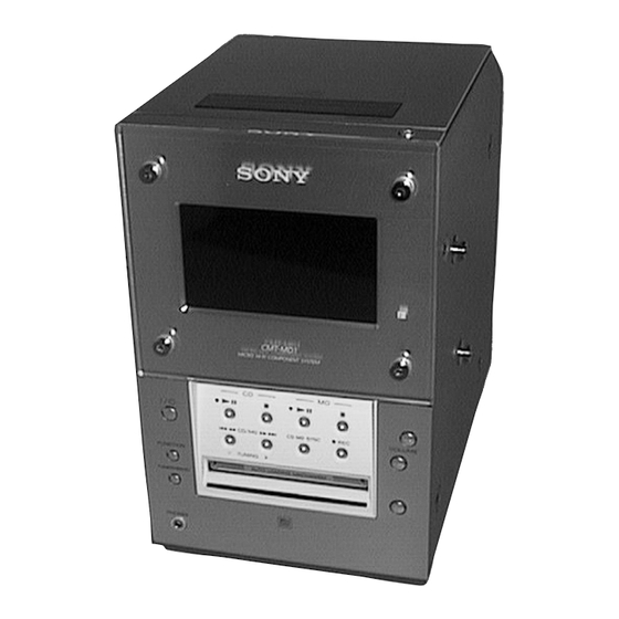
SERVICE MANUAL
Ver 1.1 2001.02
HCD-MD1EX is the Amplifier, CD player,
Mini disc Deck and Tuner section in
CMT-MD1.
U.S. and foreign patents licensed form Dolby Laboratories
Licensing Corporation.
Sony Corporation
9-922-950-12
2001B0500-1
Audio Entertainment Group
C 2001.2
General Engineering Dept.
HCD-MD1EX
Model Name Using Similar Mechanism
CD
Base Unit Name
Section
Optical Pick-up Name
Model Name Using Similar Mechanism
MD
Mechanism Name
Section
Optical Pick-up Name
SPECIFICATIONS
COMPACT Hi-Fi COMPONENT SYSTEM
US Model
Canadian Model
AEP Model
UK Model
E Model
HCD-MD333
BU-22BD19
KSS-213B/K-N
HCD-MD333
MDM-3J
KMS-260A/J1N
– Continued on next page –
Advertisement
Table of Contents

Related Manuals for Sony HCD-MD1EX - System


Summary of Contents for Sony HCD-MD1EX - System
- Page 1 Optical Pick-up Name KSS-213B/K-N Model Name Using Similar Mechanism HCD-MD333 Mechanism Name MDM-3J Section Optical Pick-up Name KMS-260A/J1N SPECIFICATIONS – Continued on next page – COMPACT Hi-Fi COMPONENT SYSTEM Sony Corporation 9-922-950-12 2001B0500-1 Audio Entertainment Group C 2001.2 General Engineering Dept.
- Page 2 – 2 –...
-
Page 3: Self-Diagnosis Function
SELF-DIAGNOSIS FUNCTION The self-diagnosis function consists of error codes for users which are displayed automatically when errors occur, and error codes which show the error history in the test mode during servicing. For details on how to view error codes for users, refer to the following box in the instruction manual. - Page 4 ITEM OF ERROR HISTORY MODE ITEMS AND CONTENTS Selecting the Test Mode Display Details of History total rec Displays the recording time in the form of “rππππππh”. The displayed time is the total number of hours the laser is high power, which is about one-fourth of the actual recording time.
-
Page 5: Table Of Contents
TABLE OF CONTENTS SELF-DIAGNOSIS FUNCTION ........3 SERVICING NOTES ..........6 GENERAL ..............9 DISASSEMBLY ............12 SERVICE MODE ............19 TEST MODE .............. 20 ELECTRICAL ADJUSTMENTS MD Section ..............26 CD Section ..............31 DIAGRAMS 7-1. Block Diagram – CD Section – ........33 7-2. -
Page 6: Servicing Notes
SCHÉMAS DE PRINCIPE, LES VUES EXPLOSÉES ET LES CRITICAL TO SAFE OPERATION. REPLACE THESE COMPO- LISTES DE PIECES NENTS WITH SONY PARTS WHOSE PART NUMBERS APPEAR AS SHOWN IN THIS MANUAL OR IN SUPPLEMENTS PUB- SONT D'UNE IMPORTANCE CRITIQUE POUR LA SÉCURITÉ DU LISHED BY SONY. - Page 7 SAFETY CHECK-OUT CAUTION After correcting the original service problem, perform the follow- Use of controls or adjustments or performance of procedures ing safety check before releasing the set to the customer: other than those specified herein may result in hazardous ra- Check the antenna terminals, metal trim, “metallized”...
- Page 8 MODEL IDENTIFICATION HOW TO OPEN THE CD LID — Bottom view — 1. Remove Side panel (L), (R). (Refer to page 12) 2. Rotate the Worm gear ass’y to direction of the arrow A. CD lid PART No. Front Panel Worm gear ass’y MODEL PART No.
-
Page 9: General
SECTION 2 GENERAL LOCATION OF CONTROLS • Front view 1(Upper panel) CD lid 6 (CD) button 2(Upper panel) Display window Remote sensor MD ^ button and indicator MD p button VOLUME +/– buttons 6 (MD) button CD p button !º CD ^ button and indicator !¡... - Page 10 • REMOTE CONTROLLER 1 2 3 4 FUNCTION button SLEEP button CD, OPEN/CLOSE button 1/u button MODE, PLAY/TUNING button REPEAT, STEREO/MONO button 9 !º !¡ VOL +/– buttons !™ !£ !¢ DBFB button BAND, TUNER button !∞ !§ !¶ –, PRESET button !•...
- Page 11 This section is extracted from instruction manual. – 11 –...
-
Page 12: Disassembly
SECTION 3 DISASSEMBLY Note: Follow the disassembly procedure in the numerical order given. PANEL, COVER 1 two screws (case 3 TP2) 5 two claws 2 two screws 6 rear cover 4 two claws 1 two screws 1 two screws (case 3 TP2) (case 3 TP2) 3 side panel (L) 2 two screws... - Page 13 CD LID OPEN/CLOSE MOTOR 3 CD lid open/close motor 2 two screws 1 belt (B 2.6 FRONT PANEL SECTION 1 connector (CN104) 3 connector (CN705) 4 front panel section 2 two screws (BV/ring) – 13 –...
- Page 14 CD BASE UNIT 3 screw (PTT 2.6 5 two screws (PTPWHM 2.6) 4 earth lug 5 two screws (PTPWHM 2.6) 6 CD base unit 2 Remove the CD base unit section to direction of the arrow A . 1 two screws 1 two screws (BVTP 2.6) (BVTP 2.6)
- Page 15 POWER BOARD 3 two screws (BVTP 3 5 connector 1 connector (CN503) 2 screw (CN501) (BVTT 3 6 Remove the POWER board to direction of the arrow A . 1 connector (CN501) 4 PC board holder MD MECHANISM DECK 3 Remove the MD mechanism deck section to direction of the arrow A .
- Page 16 BD BOARD 1 flat wire (25 core) (CN107) 5 BD (MD) board 3 screw (BVTT 2 2 flexible board (CN104) 2 flexible board (CN101) 1 flat wire (25 core) (CN106) 4 two claws SUB CHASSIS 1 two step screws 1 two step screws 2 insulator 2 insulator part A...
- Page 17 OVER WRITE HEAD 1 screw (P 1.7 2 over write head SHUTTER ASS’Y 1 stopper washer shutter ass’y 2 shaft (shutter) A shaft (shutter) B shaft (shutter) A 3 shutter ass’y hole B hole A When installing, install the shaft (shutter) A into the hole as show in the figune before installing the shaft (shutter) B into the hole B.
- Page 18 SLIDER COMPLETE ASS’Y claw 3 Set the shaft of gear (LB) to be at the position in the figure. claw 1 special screw 2 retainer (gear) (M 1.7 1.4) 4 Remove the slider complete ass’y in the direction of arrow with putting out of two claws.
-
Page 19: Service Mode
SECTION 4 SERVICE MODE Change-over of AM (MW) Tuner Step between 9 kHz and 10 kHz • A step of AM (MW) channels can be changed over between 9 kHz and 10 kHz. Procedure: 1. Press 1/u button to turn the set ON. [TUNER/BAND] 2. -
Page 20: Test Mode
SECTION 5 TEST MODE 5-1. PRECAUTIONS FOR USE OF TEST MODE Recording Laser Emission Mode • Continuous recording mode (CREC MODE) • Traverse adjustment mode (EFBAL ADJUST) • Laser power adjustment mode (LDPWR ADJUST) • Laser power check mode (LDPWR CHECK) •... - Page 21 5-5. SELECTING THE TEST MODE [VOLUME+] There are altogether 26 test modes, shown in the following table. Press the button to the mode below the current mode in the [VOLUME–] button to the mode above. Each time the ^ (CD) button is pressed, the display changes in the table while press the following order;...
- Page 22 3. Ending the continuous playback mode 1 Press the ^ (CD) button. The display changes to “CPLAY MODE”. 2 Press the 6 (MD) button to remove the disc. Note: The playback start addresses for IN, MID, and OUT are as follows. To display the playback position address on the display, press the 1/u button to display “CPLAY ( )”.
- Page 23 5-7. DISPLAYS DURING TEST MODE The display changes according to the following sequence each time the 1/u button is pressed. 1. Mode display “TEMP ADJUST” and “CPLAYMODE” are displayed. Mode display 2. Error rate display Error rate display The error rate is displayed as follows. AD = Address display C = :Indicates the C1 error.
- Page 24 5-8. AGING MODE This unit is provided with an aging mode. In this mode, MD and CD operations are performed alternately according to the following sequence. Aging will be carried out continuously unless an error occurs. If an error occurs, the status and number of cycles are displayed alternately, and operations stop. (Refer to Table 1.) Aging Mode Sequence Start Turn ON Power using function MD...
- Page 25 Procedure: 1. Load a recordable disc (MD) and CD test disc (YEDS-18). (*Note 1) [VOLUME–] button, press the )+ button. 2. While pressing the 3. Aging is executed in the above sequence. 4. To end, press the p (CD or MD) button. *Note 1: Any CD can be used, but one with a short last track is recommended.
-
Page 26: Electrical Adjustments
SECTION 6 ELECTRICAL ADJUSTMENTS Note: When performing laser power checks and adjustment (electrical MD SECTION adjustment), use of the new MD laser power meter 8010S (J-2501- 145-A) instead of the conventional laser power meter is convenient. 6-1. PRECAUTIONS FOR CHECKING LASER It sharply reduces the time and trouble to set the laser power meter DIODE EMISSINON sensor onto the objective lens of the pick-up. - Page 27 6-6. LASER POWER ADJUSTMENT 6-7. TRAVERSE ADJUSTMENT Connection : Connection : Laser power Oscilloscope meter BD (MD) board TP69 (TEO) Optical pick-up TP1003 (VC) objective lens V: 0.5 v/div H: 10 ms/div Input: DC mode Digital volt meter Adjusting Procedure: 1.
- Page 28 6-8. FOCUS BIAS ADJUSTMENT 10. Next “EFB = MO-P” is displaed, the optical pick-up moves to the internal circumference of the pit and servo is imposed. Adjusting Procedure : [VOLUME+/–] 11. Press the button so that the oscilloscope wave- 1. Load a continuously recorded disc (Refer to 6-4. Creating the form becomes the specified value.
- Page 29 6-9. ERROR RATE CHECK 6-9-1. CD Error Rate Check Checking Procedure : 1. Load a check disc (MD) TDYS-1. [VOLUME+/–] 2. Press the button to display “CPLAY MODE”. 3. Press the p (CD) button to display “CPLAY MID”. 4. “C = AD = ”...
- Page 30 6-11. ADJUSTING POINTS AND CONNECTING POINTS [BD (MD) Board] (Side A) D101 IC192 [BD (MD) Board] (Side B) TP (IOP) TP (I + 3V) Q163 IC316 IC171 TP1003 (VC) IC101 TP69 (TEO) Q102 IC121 – 30 –...
-
Page 31: Cd Section
S Curve Check CD SECTION oscilloscope Note: BD (CD) board 1. CD Block is basically designed to operate without adjustment. Therefore, check each item in order given. TP (FEO) – TP (VC) 2. Use YEDS-18 disc (3-702-101-01) unless otherwise indicated. 3. - Page 32 E-F Balance (1 Track Jump) Check Adjustment Location: (Without remote commander) [BD (CD) Board] (Side B) oscilloscope BD (CD) board TP (TEO) RV101 – TP (VC) (Focus Bias Adjustment) IC101 Procedure : RV103 1. Connect oscilloscpe to test point TP (TEO) on BD (CD) board. 2.
-
Page 33: Diagrams
HCD-MD1EX SECTION 7 DIAGRAMS 7-1. BLOCK DIAGRAM – CD Section – DIGITAL FILTER, D/A CONVERTER, FILTER RF AMP, LOW-PASS FILTER FOCUS/TRACKING/SLED SERVO IC104 DIGITAL SIGNAL IC101 PROCESSOR, CLV SERVO IC103 CLOCK XTAI 7 12 9 8 RF AMP GENERATOR X101 16.9344MHz PCMD DATA... -
Page 34: Block Diagram - Md Section
HCD-MD1EX 7-2. BLOCK DIAGRAM – MD Section – DIGITAL SIGNAL PROCESSOR, EFM/ACIRC ENCODER/DECODER, SHOCK PROOF MEMORY CONTROLLER, IC121 (1/2) ATRAC ENCODER/DECODER, 2M BIT D-RAM (Page 37) OVER WRITE IC121 (1/2) EFMO ADDT ADDT HEAD DRIVE IC181, Q181, 182 HR901 FILI OVER WRITE HEAD CLTV SAMPLING... -
Page 35: Block Diagram - Main Section
HCD-MD1EX 7-3. BLOCK DIAGRAM – MAIN Section – SIGNAL PATH A/D, D/A CONVERTER IC201 : MD PLAY AINL DECIMATION : MD REC AINR ADDT FILTER MODULATOR SDTO R-CH (Page 36) : CD PLAY DADT,BCK, : FM/AM AOUTL LRCK, FS256 SERIAL DADT SDTI MODULATOR &... -
Page 36: Block Diagram - Display/Power Supply Section
HCD-MD1EX 7-4. BLOCK DIAGRAM – DISPLAY/POWER SUPPLY Section – FLUORESCENT INDICATOR TUBE FL901 SDATA DATA 15 SCK CLOCK REMOTE CONTROL RECEIVER SIRCS IC902 RESET GRID DRIVE DIG15 Q902 FL/LED DRIVER IC901 S901 – 915 GRID DRIVE DIG1 Q901 RY501 MASTER CONTROLLER RELAY ST +12V RELAY DRIVE... -
Page 37: Note For Printed Wiring Boards And Schematic Diagrams
Circuit Boards Location 7-5. NOTE FOR PRINTED WIRING BOARDS AND SCHEMATIC DIAGRAMS Note on Schematic Diagram: Note on Printed Wiring Board: • All capacitors are in µF unless otherwise noted. pF: µµF • X : parts extracted from the component side. AMP board 50 WV or less are not indicated except for electrolytics •... -
Page 38: Printed Wiring Board – Bd (Cd) Section
HCD-MD1EX 7-6. PRINTED WIRING BOARD – BD (CD) Section – • See page 41 Circuit Boards Location. (Page 57) • Semiconductor • Semiconductor Location Location Ref. No. Location Ref. No. Location IC103 IC101 IC102 Q101 IC104 Q103 Q102 – 43 – –... -
Page 39: Schematic Diagram - Bd (Cd) Section
HCD-MD1EX 7-7. SCHEMATIC DIAGRAM – BD (CD) Section – • See page 77 for Waveforms. • See page 79 for IC Block Diagrams. (Page 59) • Voltages and waveforms are dc with respect to ground under no-signal conditions. no mark : STOP ) : CD PLAY : Impossible to measure The components identified by mark ! or dotted... -
Page 40: Printed Wiring Board – Bd (Md) Section
HCD-MD1EX 7-8. PRINTED WIRING BOARD – BD (MD) Section – • See page 41 Circuit Boards Location. (Page 75) (Page 57) • Semiconductor • Semiconductor Location Location Ref. No. Location Ref. No. Location D101 D181 D183 IC192 IC401 IC101 IC103 IC121 IC124 IC152... -
Page 41: Schematic Diagram – Bd (Md) Section (1/3)
HCD-MD1EX 7-9. SCHEMATIC DIAGRAM – BD (MD) Section (1/3) – • See page 77 for Waveforms. • See page 82 for IC Block Diagrams. (Page 52) (Page 52) (Page 51) (Page 51) • Voltages and waveforms are dc with respect to ground under no-signal conditions. -
Page 42: Schematic Diagram - Bd (Md) Section (1/3)
HCD-MD1EX • Voltages and waveforms are dc with respect to ground under no-signal conditions. no mark : STOP ) : MD PLAY ] : MD REC 7-10. SCHEMATIC DIAGRAM – BD (MD) Section (2/3) – • See page 77 for Waveforms. •... -
Page 43: Schematic Diagram - Bd (Md) Section (2/3)
HCD-MD1EX 7-11. SCHEMATIC DIAGRAM – BD (MD) Section (3/3) – • See page 77 for Waveforms. • See page 82 for IC Block Diagrams. (Page 52) (Page 51) (Page 51) (Page 76) • Voltages and waveforms are dc with respect to ground under no-signal conditions. -
Page 44: Printed Wiring Board - Main Board (Side A)
HCD-MD1EX 7-12. PRINTED WIRING BOARD – MAIN Board (side A) – • See page 41 Circuit Boards Location. – 55 – – 56 –... -
Page 45: Printed Wiring Board – Main Board (Side B)
HCD-MD1EX 7-13. PRINTED WIRING BOARD – MAIN Board (side B) – • See page 41 Circuit Boards Location. (Page 72) • Semiconductor Location Ref. No. Location D701 D702 D703 D704 D705 D707 D708 D709 D710 D711 D712 D713 (Page 64) D714 D715 D716... -
Page 46: Schematic Diagram - Main Section (1/2)
HCD-MD1EX • Voltages and waveforms are dc with respect to ground under no-signal (detuned) conditions. no mark : FM 7-14. SCHEMATIC DIAGRAM – MAIN Section (1/2) – • See page 78 for Waveforms. • See page 84 for IC Block Diagrams. : Impossible to measure (Page 46) (Page 61) -
Page 47: Schematic Diagram - Main Section (2/2)
HCD-MD1EX 7-15. SCHEMATIC DIAGRAM – MAIN Section (2/2) – • See page 78 for Waveforms. • See page 84 for IC Block Diagrams. (Page (Page 74) (Page 60) (Page 65) • Voltages and waveforms are dc with respect to ground under no-signal (detuned) conditions. -
Page 48: Printed Wiring Boards – Panel Section
HCD-MD1EX 7-16. PRINTED WIRING BOARDS – PANEL Section – • See page 41 Circuit Boards Location. (Page 57) (Page 64) (Page 63) (Page 68) • Semiconductor Location Ref. No. Location Ref. No. Location D901 Q901 D902 Q902 D903 Q903 D905 Q904 D907 Q905... -
Page 49: Schematic Diagram - Panel Section
HCD-MD1EX 7-17. SCHEMATIC DIAGRAM – PANEL Section – • See page 85 for IC Block Diagrams. (Page 70) (Page 62) • Voltages and waveforms are dc with respect to ground under no-signal (detuned) conditions. no mark : FM – 65 – –... -
Page 50: Printed Wiring Boards - Amp/Transformer Section
HCD-MD1EX 7-18. PRINTED WIRING BOARDS – AMP/TRANSFORMER Section – • See page 41 Circuit Boards Location. (Page 72) (Page 64) (Page 68) (Page 68) (Page 72) (Page 72) – 67 – – 68 –... -
Page 51: Schematic Diagram - Amp/Transformer Section
HCD-MD1EX 7-19. SCHEMATIC DIAGRAM – AMP/TRANSFORMER Section – (Page 74) (Page 74) (Page 73) (Page 66) • Voltages and waveforms are dc with respect to ground under no-signal (detuned) conditions. no mark : FM The components identified by mark ! or dotted Les composants identifiés par une marque ! sont line with mark ! are critical for safety. -
Page 52: Printed Wiring Board - Power Section
HCD-MD1EX 7-20. PRINTED WIRING BOARD – POWER Section – • See page 41 Circuit Boards Location. (Page 68) (Page • Semiconductor Location (Page 57) (Page 68) Ref. No. Location Ref. No. Location D501 IC501 D502 IC502 D503 IC503 D504 IC504 D505 IC505 D506... -
Page 53: Schematic Diagram - Power Section
HCD-MD1EX 7-21. SCHEMATIC DIAGRAM – POWER Section – (Page 62) (Page 69) (Page 69) (Page 69) • Voltages and waveforms are dc with respect to ground under no-signal (detuned) conditions. The components identified by mark ! or dotted Les composants identifiés par une marque ! sont no mark : FM line with mark ! are critical for safety. -
Page 54: Printed Wiring Boards - Motor/Sw Section
HCD-MD1EX 7-22. PRINTED WIRING BOARDS – MOTOR/SW Section – 7-23. SCHEMATIC DIAGRAM – MOTOR/SW Section – (Page 57) (Page 57) (Page 60) (Page 60) (Page 48) (Page 54) – 75 – – 76 –... - Page 55 • Waveforms – BD (CD) Board – – BD (MD) Board – 1 IC101 #¡ (RFO) (CD Play Mode) 1 IC101 1, 2 (I, J) (MD Play Mode) 6 IC103 @∞ (XPCK) 500 mV/DIV, 500 ns/DIV Approx. 5.3 Vp-p 500 mVp-p 0.3 Vp-p 14 ns 2 IC101 $¢...
- Page 56 – MAIN Board – 6 IC152 #¡ (CAPA+) (MD Play Mode) !¡ IC121 @¶ (FS256) 1 IC707 !¡ (X1) 4.6 Vp-p 3.4 Vp-p 3.8 Vp-p 11.2896 MHz 5 MHz 1.5 sec 7 IC121 (º (FS4) !™ IC316 !£ (XOUT) 2 IC707 !¢ (XT1) 2.4 Vp-p 3.4 Vp-p 3.3 Vp-p...
- Page 57 • IC Block Diagrams – BD (CD) Board – IC101 CXA1782BQ – LEVELS 24 SENS – MIRR RF IV AMP1 DFCT 23 C. OUT – 22 XRST RF IV AMP2 21 DATA FE BIAS • IIL DATA RESISTOR • INPUT SHIFT RESISTOR •...
- Page 58 IC102 BA6397FP DRIVE DRIVE DRIVE BUFFER BUFFER BUFFER DRIVE BUFFER REGULATOR DRIVER MUTE DRIVE DRIVE DRIVE DRIVE BUFFER BUFFER BUFFER BUFFER IC103 CXD2507AQ SERVO AUTO DATA SEQUENCER XRST SENS SUB CODE MUTE INTERFACE PROCESSOR DIGITAL LOCK SQCK TEST SQSO FILO EXCK DIGITAL FILI...
- Page 59 IC104 PCM1710U-B LRCIN ML/DSD INPUT MC/DM2 INTERFACE DIGITAL MODE FILTER CONTROL BCKIN MD/DM1 TIMING CLKO MUTE CONTROL MODE CKSL NOISE SHAPER DGND DGND 5-LEVEL DAC 5-LEVEL DAC RIGHT LEFT GND2R GND2L LOW-PASS FILTER LOW-PASS FILTER LEFT RIGHT EXT1R EXT1L 3-STAGE AMP 3-STAGE AMP EXT2R EXT2L...
- Page 60 – BD (MD) Board – IC101 CXA2523AR 43 42 USROP – RF AGC – USRC RFA1 BPF3T RFA2 RFA3 PEAK3T – HLPT –1 – – –2 – OFST PTGR TEMP PEAK – –2 – 36 BOTM BOTTOM – –1 – GRVA PBSW 35 ABCD...
- Page 61 IC121 CXD2652AR 100 99 98 97 96 95 94 93 92 91 90 89 88 87 86 85 84 83 82 81 80 79 78 77 76 75 AUX2 SPINDLE GENERATOR SERVO 74 TE MNT0 73 SE MNT1 MONITOR EACH 72 AVSS CONTROL BLOCK...
-
Page 62: Main Board
IC153 LB1830M-S-TE-L IC201 AK4520A-VF-E2 VREF VCONT VREF LOGIC CLOCK PREDRIVER MODULATOR INTERPOLATOR DIVIDER MODULATOR INTERPOLATOR COMMON SERIAL I/O VOLTAGE INTERFACE DECIMATION MODULATOR FILTER DECIMATION MODULATOR FILTER OUT2 OUT1 VS 9 10 – MAIN Board – IC702 LB1641 IC706 M62016L T.S.D O.C.P INTERRUPT SIGNAL MOTOR... -
Page 63: Panel Board
IC710 BU1922-E2 (AEP, UK) TEST LOGIC AND OUTPUT SELECTOR SWITCH 57kHz ANTI- OSCILLATOR QUALITY BIT RECONSTRUCTION BANDPASS ALIASING GENERATOR FILTER (8th ORDER) DIVIDER FILTER BIPHASE CONTAS LOOP DEFFERENTIAL CLOCKED SYMBOL VARIABLE AND DECODER COMPARATOR DECODER FIXED DIVIDER CLOCK REGENERATION AND SYNC REFERENCE VOLTAGE –... -
Page 64: Ic Pin Function Description
7-24. IC PIN FUNCTION DESCRIPTION BD (MD) BOARD IC101 CXA2523AR (RF AMP, FOCUS/TRACKING ERROR AMP) Pin No. Pin Name Function I-V converted RF signal I input from the optical pick-up block detector I-V converted RF signal J input from the optical pick-up block detector Middle point voltage (+1.65V) generation output terminal 4 to 9 A to F... - Page 65 BD (MD) BOARD IC121 CXD2652AR (DIGITAL SIGNAL PROCESSOR, DIGITAL SERVO PROCESSOR, EFM/ACIRC ENCODER/DECODER, SHOCK PROOF MEMORY CONTROLLER, ATRAC ENCODER/DECODER, 2M BIT D-RAM) Pin No. Pin Name Function Focus OK signal output to the MD mechanism controller (IC316) MNT0 (FOK) “H” is output when focus is on (“L”: NG) MNT1 (SHCK) Track jump detection signal output to the MD mechanism controller (IC316) MNT2 (XBUSY)
- Page 66 Pin No. Pin Name Function Two-way data bus with the D-RAM (IC124) MVCI Digital in PLL oscillation input from the external VCO Not used (fixed at “L”) ASYO Playback EFM full-swing output terminal ASYI I (A) Playback EFM asymmetry comparator voltage input terminal AVDD —...
- Page 67 Pin No. Pin Name Function SPRD Spindle servo drive PWM signal (–) output to the BH6511FS (IC152) SPFD Spindle servo drive PWM signal (+) output to the BH6511FS (IC152) FGIN TEST1 Input terminal for the test (fixed at “L”) TEST2 TEST3 DVSS —...
- Page 68 BD (MD) BOARD IC316 M30610MCA-272FP (MD MECHANISM CONTROLLER) Pin No. Pin Name Function JOG0 Rotary encoder jog dial pulse input terminal Not used (fixed at “H”) JOG1 Rotary encoder jog dial pulse input terminal Not used (fixed at “H”) DAOUT0 Monitor output terminal for the test C1 error rate is output when test mode DAOUT1 Monitor output terminal for the test ADER is output when test mode...
- Page 69 Pin No. Pin Name Function SENS Internal status (SENSE) input from the CXD2652AR (IC121) Recording data output enable signal output to the CXD2652AR (IC121) and overwrite head SCTX driver (IC181) Writing data transmission timing output (Also serves as the magnetic head on/off output) XINT Not used (pull down)
- Page 70 Pin No. Pin Name Function 81, 82 — Not used (fixed at “L”) POWER Power on/off control signal output terminal Not used (pull down) 84 to 90 — Not used (fixed at “L”) 91 to 93 KEY0 to KEY2 Key input terminal (A/D input) Not used (fixed at “H”) —...
- Page 71 MAN BOARD IC707 PD78078GF-083-3BA (MASTER CONTROLLER (CD MECHANISM CONTROL/SYSTEM CONTROL)) Pin No. Pin Name Function Destination setting terminal Not used (open) Destination setting terminal US, Canadian models: fixed at “L”, Other models: open Destination setting terminal US, Canadian, Singapore, Hong Kong models: fixed at “L”, Other models: open Destination setting terminal Not used (open) 5 to 7 Not used (open)
- Page 72 Pin No. Pin Name Function RESET Reset signal output to the FL driver (IC901) “L”: reset SUBQ Subcode Q data input from the CXD2507AQ (IC103) Not used (open) SQCLK Subcode Q data reading clock signal output to the CXD2507AQ (IC103) CLOCK Serial data transfer clock signal output to the CXD2507AQ (IC103) and PCM1710U (IC104) DATA...
- Page 73 Pin No. Pin Name Function PLL serial chip enable signal output to the FM/AM tuner unit ST-MUTE Tuner muting on/off control signal output to the FM/AM tuner unit “L”: muting on FM/AM SELECT FM/AM selection signal output terminal Not used (open) SIRCS Sircs signal input from the remote control receiver (IC902) —...
-
Page 74: Exploded Views
SECTION 8 EXPLODED VIEWS NOTE: • -XX and -X mean standardized parts, so they • Items marked “*” are not stocked since they The components identified by mark ! or dotted line with mark may have some difference from the original are seldom required for routine service. - Page 75 (2) FRONT PANEL SECTION Ref. No. Part No. Description Remark Ref. No. Part No. Description Remark 4-212-503-01 PLATE (BUTTON), ORNAMENTAL * 57 A-4417-231-A PANEL BOARD, COMPLETE 4-212-531-01 SCREW * 58 1-671-424-11 HP BOARD 4-212-103-01 PLATE (GLASS), ORNAMENTAL 4-212-533-01 BUTTON (VOL) 4-212-502-01 PLATE (INDICATION WINDOW) X-4950-365-1 PANEL ASSY, FRONT 4-212-532-01 BUTTON (POWER) (+, –, §)
- Page 76 (3) CD SECTION not supplied not supplied not supplied not supplied not supplied BU-22BD19 M103 not supplied Ref. No. Part No. Description Remark Ref. No. Part No. Description Remark * 101 1-671-426-11 EJECT BOARD 4-212-525-01 WINDOW (CD) 4-212-497-01 TABLE, DISC 4-212-504-01 PLATE (LID), ORNAMENTAL 4-951-620-41 SCREW (2.6), +BVTP 4-212-495-01 ARM, CHUCKING...
- Page 77 (4) CHASSIS SECTION T901 not supplied M501 not supplied US/CND supplied not supplied MDM-3J AEP, SP, HK not supplied The components identified by Les composants identifiés par une mark ! or dotted line with marque ! sont critiques pour la mark ! are critical for safety.
- Page 78 (5) MD MECHANISM DECK SECTION-1 (MDM-3J) not supplied Ref. No. Part No. Description Remark Ref. No. Part No. Description Remark * 201 A-4699-808-A BD (MD) BOARD, COMPLETE 4-986-959-01 WASHER, STOPPER 1-660-966-11 OP RELAY FLEXIBLE BOARD 4-987-327-01 INSULATOR 1-782-683-11 WIRE (FLAT TYPE) (14 CORE) 4-628-167-01 SCREW, STEP X-4949-900-1 SHUTTER ASSY 4-997-962-01 SPRING (O/C), TENSION...
- Page 79 HCD-MD1EX Ver 1.1 2001.02 (6) MD MECHANISM DECK SECTION-2 (MDM-3J) not supplied not supplied M903 M902 M901 HR901 The components identified by Les composants identifiés par une mark 0 or dotted line with marque 0 sont critiques pour la mark 0 are critical for safety. sécurité.
- Page 80 (7) CD BASE UNIT SECTION (BU-22BD19) M101 M102 The components identified by Les composants identifiés par une mark ! or dotted line with marque ! sont critiques pour la mark ! are critical for safety. sécurité. Replace only with part num- Ne les remplacer que par une pièce ber specified.
-
Page 81: Electrical Parts List
SECTION 9 BD (CD) ELECTRICAL PARTS LIST NOTE: • Due to standardization, replacements in the • Items marked “*” are not stocked since they The components identified by mark ! or dotted line with mark are seldom required for routine service. parts list may be different from the parts speci- ! are critical for safety. - Page 82 BD (CD) BD (MD) Ref. No. Part No. Description Remark Ref. No. Part No. Description Remark C154 1-163-235-11 CERAMIC CHIP 22PF R144 1-216-073-00 METAL CHIP 1/10W < CONNECTOR > R145 1-216-097-00 RES, CHIP 100K 1/10W R146 1-216-097-00 RES, CHIP 100K 1/10W CNU101 1-770-014-11 CONNECTOR, FFC/FPC 16P R147...
- Page 83 BD (MD) Ref. No. Part No. Description Remark Ref. No. Part No. Description Remark C131 1-163-023-00 CERAMIC CHIP 0.015uF C363 1-163-251-11 CERAMIC CHIP 100PF C132 1-107-823-11 CERAMIC CHIP 0.47uF C133 1-163-017-00 CERAMIC CHIP 0.0047uF 5% C401 1-163-038-00 CERAMIC CHIP 0.1uF C134 1-163-038-00 CERAMIC CHIP 0.1uF...
- Page 84 BD (MD) Ref. No. Part No. Description Remark Ref. No. Part No. Description Remark Q103 8-729-028-99 TRANSISTOR RT1N144M-TP-1 R189 1-216-073-00 METAL CHIP 1/10W Q104 8-729-028-99 TRANSISTOR RT1N144M-TP-1 Q162 8-729-101-07 TRANSISTOR 2SB798-DL R190 1-216-073-00 METAL CHIP 1/10W R195 1-216-295-00 SHORT Q163 8-729-028-91 TRANSISTOR DTA144EUA-T106 R196 1-216-295-00 SHORT...
- Page 85 BD (MD) EJECT JOINT Ref. No. Part No. Description Remark Ref. No. Part No. Description Remark R442 1-216-097-00 RES, CHIP 100K 1/10W < DIODE > R443 1-216-097-00 RES, CHIP 100K 1/10W R444 1-216-097-00 RES, CHIP 100K 1/10W D906 8-719-069-45 LED SELU5E23C-TP15 R445 1-216-097-00 RES, CHIP 100K...
- Page 86 JOINT MAIN Ref. No. Part No. Description Remark Ref. No. Part No. Description Remark R547 1-216-077-00 METAL CHIP 1/10W C751 1-163-009-11 CERAMIC CHIP 0.001uF C752 1-104-664-11 ELECT 47uF < SWITCH > C753 1-130-477-00 MYLAR 0.0033uF 5% ! S101 1-572-675-11 SWITCH, POWER VOLTAGE CHANGE C754 1-104-664-11 ELECT 47uF...
- Page 87 MAIN Ref. No. Part No. Description Remark Ref. No. Part No. Description Remark C807 1-163-239-11 CERAMIC CHIP 33PF IC704 8-759-269-09 IC SN74HCT04ANS (AEP, UK) IC705 8-759-494-40 IC M62428AFP600C C808 1-163-021-11 CERAMIC CHIP 0.01uF IC706 8-759-481-02 IC M62016L (AEP, UK) IC707 8-759-545-08 IC uPD78078GF-083-3BA C809 1-163-009-11 CERAMIC CHIP...
- Page 88 MAIN Ref. No. Part No. Description Remark Ref. No. Part No. Description Remark R715 1-216-077-00 METAL CHIP 1/10W R772 1-216-065-00 RES, CHIP 4.7K 1/10W R773 1-216-061-00 METAL CHIP 3.3K 1/10W R716 1-216-065-00 RES, CHIP 4.7K 1/10W R774 1-216-041-00 METAL CHIP 1/10W R717 1-216-065-00 RES, CHIP...
- Page 89 MAIN MOTOR PANEL Ref. No. Part No. Description Remark Ref. No. Part No. Description Remark R826 1-216-049-11 RES, CHIP 1/10W < CONNECTOR > R827 1-216-073-00 METAL CHIP 1/10W R828 1-216-081-00 METAL CHIP 1/10W CN901 1-779-969-11 PLUG, CONNECTOR (PC BOARD) 24P R829 1-216-049-11 RES, CHIP 1/10W...
- Page 90 PANEL POWER Ref. No. Part No. Description Remark Ref. No. Part No. Description Remark R929 1-216-045-00 METAL CHIP 1/10W C522 1-126-916-11 ELECT 1000uF 6.3V C523 1-126-933-11 ELECT 100uF R930 1-216-037-00 METAL CHIP 1/10W C524 1-126-933-11 ELECT 100uF R931 1-216-049-11 RES, CHIP 1/10W C525 1-163-021-11 CERAMIC CHIP...
- Page 91 POWER SENSOR Ref. No. Part No. Description Remark Ref. No. Part No. Description Remark ! F503 1-576-105-11 FUSE (2.5A/250V) (US, CND) ! R536 1-249-387-11 CARBON 1/4W F < GROUND TERMINAL > R537 1-216-057-00 METAL CHIP 2.2K 1/10W R538 1-216-091-00 METAL CHIP 1/10W EPT501 1-537-771-21 TERMINAL BOARD, GROUND R539...
- Page 92 ! are critical for safety. sécurité. Replace only with part num- Ne les remplacer que par une pièce ber specified. portant le numéro spécifié. Sony Corporation 98H0586-1 Printed in Japan © 1998. 8 9-922-950-11 Home A&V Products Company Published by Quality Assurance Dept.
- Page 93 HCD-MD1EX MEMO...
-
Page 94: Revision History
HCD-MD1EX REVISION HISTORY Clicking the version allows you to jump to the revised page. Also, clicking the version at the upper right on the revised page allows you to jump to the next revised page. Ver. Date Description of Revision 2001.02 Correction of Motor (M902, M903) (SPM-01004)
Need help?
Do you have a question about the HCD-MD1EX - System and is the answer not in the manual?
Questions and answers