Table of Contents
Advertisement
Quick Links
SERVICE MANUAL
Ver 1.0 2001.04
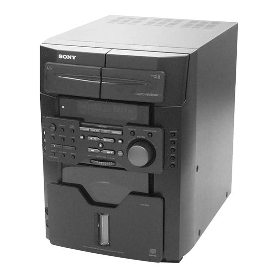
HCD-MG510AV are the Amplifier, CD player, Tape
Deck and Tuner section in MHC-MG510AV.
This stereo system is equipped with the Dolby* Pro Logic
Surround decoder.
* Manufactured under license from Dolby Laboratories.
Dolby , Pro Logic , and the double-D symbol ; are
trademarks of Dolby Laboratories. Confidential
unpublished works. '1992-1997 Dolby Laboratories.
All rights reserved.
Amplifier section
AUDIO POWER SPECIFICATIONS
POWER OUTPUT AND TOTAL
HARMONIC DISTORTION:
with 8 ohm loads both channels driven, from
120 – 10,000 Hz; rated 75 watts per channel
minimum RMS power, with no more than 10%
total harmonic distortion from 250 milliwatts to
rated output.
Front speaker:
Continuous RMS power output
75 + 75 watts
(8 ohms at 1 kHz,
10% THD)
Total harmonic distortion less than 0.09%
(8 ohms at 1 kHz,
40 watts)
Center speaker:
Continuous RMS power output
45 watts
(8 ohms at 1 kHz,
10% THD)
Rear speaker:
Continuous RMS power output
45 + 45 watts
(8 ohms at 1 kHz,
10% THD)
Sub woofer:
Continuous RMS power output
45 watts
(8 ohms at 100 Hz,
10% THD)
Sony Corporation
9-873-812-11
2001D0500-1
Home Audio Company
C 2001.4
Shinagawa Tec Service Manual Production Group
HCD-MG510AV
Model Name Using Similar Mechanism
CD Mechanism Type
CD
Section
Base Unit Name
Optical Pick-up Name
Model Name Using Similar Mechanism
TAPE
Section
Tape Transport Mechanism Type
SPECIFICATIONS
Inputs
VIDEO/MD IN (phono jacks):
voltage 250 mV/450 mV,
impedance 47 kilohms
5.1CH:
FRONT (phono jacks):
voltage 450 mV,
impedance 47 kilohms
REAR (phono jacks):
voltage 450 mV,
impedance 47 kilohms
CENTER (phono jack):
voltage 450 mV,
impedance 47 kilohms
SUB WOOFER (phono jack):
voltage 450 mV,
impedance 47 kilohms
Outputs
PHONES (stereo phone jack):
accepts headphones of
8 ohms or more
FRONT SPEAKER:
accepts impedance of 8 to
16 ohms
SURROUND SPEAKER REAR:
accepts impedance of 8 to
16 ohms
SURROUND SPEAKER CENTER:
accepts impedance of
8 ohms
SURROUND SPEAKER SUB WOOFER:
accepts impedance of
8 ohms
COMPACT DISC DECK RECEIVER
US Model
HCD-MG310AV
CDM64-K1BD44A
BU-K1BD44A
KSM-213BFN
HCD-MG310AV
CM8L6Z511A
CD player section
System
Compact disc and digital
audio system
Laser
Semiconductor laser
(λ = 780 nm)
Emission duration:
continuous
Frequency response
2 Hz – 20 kHz (±0.5 dB)
Wavelength
780 – 790 nm
Signal-to-noise ratio
More than 90 dB
Dynamic range
More than 90 dB
OPTICAL OUT (CD)
(Square optical connector jack, rear panel)
Wavelength
660 nm
Output Level
–18 dBm
Tape player section
Recording system
4-track 2-channel stereo
Frequency response
40 – 13,000 Hz (±3 dB),
using Sony TYPE I
cassette
±0.15% W.Peak (IEC)
Wow and flutter
0.1% W.RMS (NAB)
±0.2% W.Peak (DIN)
– Continued on next page –
Advertisement
Table of Contents

Subscribe to Our Youtube Channel
Related Manuals for Sony HCD-MG510AV


Summary of Contents for Sony HCD-MG510AV
-
Page 1: Specifications
HCD-MG510AV SERVICE MANUAL US Model Ver 1.0 2001.04 HCD-MG510AV are the Amplifier, CD player, Tape Deck and Tuner section in MHC-MG510AV. This stereo system is equipped with the Dolby* Pro Logic Model Name Using Similar Mechanism HCD-MG310AV Surround decoder. * Manufactured under license from Dolby Laboratories. -
Page 2: Table Of Contents
HCD-MG510AV Tuner section General AM tuner section Tuning range 530 – 1,710 kHz FM stereo, FM/AM superheterodyne tuner Power requirements 120 V AC, 60 Hz (with the interval set at 10 kHz) FM tuner section Power consumption 220 watts 531 – 1,710 kHz Tuning range 87.5 –... -
Page 3: Leakage Test
LINE WITH MARK 0 ON THE SCHEMATIC DIAGRAMS AND IN THE PARTS LIST ARE CRITICAL TO SAFE OPERATION. REPLACE THESE COMPONENTS WITH SONY PARTS WHOSE PART NUMBERS APPEAR AS SHOWN IN THIS MANUAL OR IN SUPPLEMENTS PUB- LISHED BY SONY. -
Page 4: Servicing Notes
HCD-MG510AV SECTION 1 SERVICING NOTES CD-TEXT TEST DISC CLEANING OBJECTIVE LENS OF OPTICAL PICK-UP • In cleaning the objective lens of optical pick-up, be sure the following below. This unit is able to display the test data (character information) written in the CD on its fluorescent indicator tube. -
Page 5: General
HCD-MG510AV SECTION 2 This section is extracted from instruction manual. GENERAL Parts Identification The items are arranged in alphabetical order. Refer to the pages indicated in parentheses ( ) for details. Main unit 2 3 4 56 7 8 w; ql 5.1CH/VIDEO (MD) 5 (28) -
Page 6: Setting The Time
HCD-MG510AV Setting the time Remote Control Turn on the system. Press TIMER SET. When you set the clock for the first time, go 1 2 3 4 5.1CH wa (30) to step 5. CD ql (14, 21) CENTER +/– 5 (11) Press –... -
Page 7: Disassembly
HCD-MG510AV SECTION 3 DISASSEMBLY • This set can be disassembled in the order shown below. 3-1. DISASSEMBLY FLOW 3-2. UPPER COVER (Page 8) 3-3. FRONT BLOCK ASSY (Page 8) 3-4. MAIN BOARD 3-13. CASSETTE LID ASSY (A)/(B) (Page 9) (Page 13) 3-5. -
Page 8: Upper Cover
HCD-MG510AV Note: Follow the disassembly procedure in the numerical order given. 3-2. UPPER COVER 2 five screws 3 upper cover (BVTP3 × 8) 2 two screws (BVTP3 × 8) 1 three screws (BVTP3 × 8) 1 three screws (BVTP3 × 8) 3-3. -
Page 9: Main Board
HCD-MG510AV 3-4. MAIN BOARD 3 two screws (BVTP3 × 8) 3 three screws (BVTP3 × 8) 1 wire (flat type) (18 core) (CN309) 1 wire (flat type) (21 core) (CN303) 2 two connectors (CN304, 903) 5 MAIN board 2 connector... -
Page 10: Main Amp Board, Power Board
HCD-MG510AV 3-6. MAIN AMP BOARD, POWER BOARD 2 four screws (BVTP3 × 8) 1 connector (CN502) 4 three screws (BVTP3 × 8) 3 MAIN AMP board 2 two screws (BVTP3 × 8) 5 center bracket 7 POWER board 6 two screws (BVTP4 ×... -
Page 11: Cd Mechanism Deck (Cdm64-K1Bd44A)
HCD-MG510AV 3-8. CD MECHANISM DECK (CDM64-K1BD44A) 5 CD mechanism deck (CDM64-K1BD44A) 1 screw (2.6 × 8) 2 table (60) 4 two screws (BVTP3 × 8) lower chassis 3 screw (PSW3 × 6) 4 four screws 4 four screws (BVTP3 × 8) (BVTP3 ×... -
Page 12: Bu Holder Assy
HCD-MG510AV 3-10. BU HOLDER ASSY 1 tension spring (F1) 2 tension spring (F-2) 3 two screws (PTP2.6 × 8) 4 BU holder assy 3 two screws (PTP2.6 × 8) 3-11. MOTOR GEAR ASSY (SLED) (M102), CD BOARD 7 gear 8 claw... -
Page 13: Op Base Assy (Ksm-213Bfn)
HCD-MG510AV 3-12. OP BASE ASSY (KSM-213BFN) 3 Remove the optical pick-up (KSM-213BFN) in the direction of arrow B . 2 sled shaft 1 Slide the lever in the direction of arrow A . 3-13. CASSETTE LID ASSY (A) / (B) 1 Open the cassette lid assy (A)/(B). -
Page 14: Mech Deck (Tape)
HCD-MG510AV 3-14. MECH DECK (TAPE) 1 three screws (BVTP3 × 10) qs mech deck (tape) 0 two screws (BVTP2.6) qa MD bracket 4 cassette holder assy (A) 2 two screws (BVTP3 × 10) 9 TC board 5 cassette 8 screw (BVTP2.6) -
Page 15: Mechanical Adjustments
HCD-MG510AV SECTION 4 MECHANICAL ADJUSTMENTS • TAPE MECHANISM DECK SECTION Torque Measurement Precaution Mode Torque meter Meter reading 1. Clean the following parts with a denatured alcohol-moistened 2.94 mN • m to 7.84 mN • m swab: CQ-102C 31 to 71 g • cm... - Page 16 HCD-MG510AV MEMO...
-
Page 17: Diagrams
HCD-MG510AV SECTION 5 DIAGRAMS 5-1. BLOCK DIAGRAM – CD SERVO Section – FILTER DIGITAL SIGNAL PROCESSOR, DIGITAL FILTER, D/A CONVERTER IC101 (1/2) RF AMP, 56 53 FOCUS/TRACKING ERROR AMP IC103 DETECTOR CD +5V PCMD LRCK INTERFACE C2PO RFAC RFAC RFAC... -
Page 18: Block Diagram - Tuner/Tape Deck Section
HCD-MG510AV 5-2. BLOCK DIAGRAM – TUNER/TAPE DECK Section – TUNER PACK TUNER L-CH (Page 19) FM ANT L-CH FM 75Ω ANT GND R-CH R-CH AM ANT ANT GND TU-CLK TU-CE TUNED TUNED 5.1CH (Page 19) INPUT SELECT SWITCH IC306 PB AMP... -
Page 19: Block Diagram - Surround Section
HCD-MG510AV 5-3. BLOCK DIAGRAM – SURROUND Section – LOW-PASS SPE ANA (Page 21) FILTER IC304 (1/2) R-CH DOLBY PRO LOGIC SURROUND PROCESSOR R-CH IC301 L-CH (Page 18) WOOFER SWVOL SWIN TRIMMER, BAND-PASS SWVOL OUT VOLUME (Page 20) FILTER IC304 (2/2) -
Page 20: Block Diagram - Amp Section
HCD-MG510AV 5-4. BLOCK DIAGRAM – AMP Section – J503 PHONE J501 (1/2) FRONT L-CH DBFB AMP (Page 19) IC303 POWER AMP – FRONT SPEAKER IC501 IMPEDANCE R-CH USE 8Ω – RY501 MUTING MUTING OVER LOAD DBFB DBFB LEVEL Q517, 518... -
Page 21: Block Diagram - Display/Power Supply Section
HCD-MG510AV 5-5. BLOCK DIAGRAM – DISPLAY/POWER SUPPLY Section – GRID DRIVE LED DRIVE D703 – 707 Q721 – 723 Q713 – 717 LED DRIVE D708, 736, FL701 Q702 – 705, 718 D781, 782, 791 FLUORESCENT INDICATOR TUBE S701, 741 – 745,... -
Page 22: Note For Printed Wiring Boards And Schematic Diagrams
HCD-MG510AV 5-6. NOTE FOR PRINTED WIRING BOARDS AND SCHEMATIC DIAGRAMS • Circuit Boards Location (In addition to this, the necessary note is printed in each block) Note on Schematic Diagram: Note on Printed Wiring Boards: • All capacitors are in µF unless otherwise noted. pF: µµF •... - Page 23 HCD-MG510AV • IC Block Diagrams IC103 CXA2581N-T4 – CD Board – RW/ROM IC101 CXD3017Q DC OFST RFDCI – – RFDCO ERROR DIGITAL CORRECTOR DIGITAL ASYMMETRY CORRECTOR – RW/ROM VOFST OPERATIONAL LRCK AMPLIFIER ANALOG SWITCH PCMD INTERFACE DEMODULATOR CONVERTER EMPH APC AMP...
-
Page 24: Schematic Diagram - Cd Section
HCD-MG510AV 5-7. SCHEMATIC DIAGRAM – CD Section – • • See page 35 for Waveforms. See page 23 for IC Block Diagrams. (Page 32) • Voltages and waveforms are dc with respect to ground The components identified by mark 0 or dotted under no-signal conditions. -
Page 25: Printed Wiring Board - Cd Section
HCD-MG510AV 5-8. PRINTED WIRING BOARD – CD Section – • See page 22 for Circuit Boards Location. OPTICAL PICK-UP BLOCK KSM-213BFN CD BOARD M101 (SPINDLE) S101 (LIMIT) (VC) M102 (SLED) TP (RFAC) TP (FE) MAIN BOARD TP (TE) CN303 (Page 34) -
Page 26: Printed Wiring Boards - Cd Motor/Sensor Section
HCD-MG510AV 5-9. PRINTED WIRING BOARDS – CD MOTOR/SENSOR Section – • See page 22 for Circuit Boards Location. (Page 34) MAIN BOARD CN305 T SENSOR BOARD L. T MOTOR BOARD 1 2 3 4 5 (LOADING) (TABLE) (11) 1-680-797- 4 3 2 1... -
Page 27: Schematic Diagram - Cd Motor/Sensor Section
HCD-MG510AV 5-10. SCHEMATIC DIAGRAM – CD MOTOR/SENSOR Section – (Page 32) (Page 32) (Page 32) (Page 32) (Page 32) • Voltages and waveforms are dc with respect to ground under no-signal conditions. no mark : CD... -
Page 28: Printed Wiring Board - Tc Section
HCD-MG510AV 5-11. PRINTED WIRING BOARD – TC Section – • See page 22 for Circuit Boards Location. MAIN BOARD (Page 34) CN311 TC BOARD 1-680-807- (11) HP101 PB HEAD (DECK A) HRPE101 REC/PB/ERASE HEAD (DECK B) • Semiconductor Location Ref. No. -
Page 29: Schematic Diagram - Tc Section
HCD-MG510AV 5-12. SCHEMATIC DIAGRAM – TC Section – • See page 39 for IC Block Diagram. (Page 30) • Voltages and waveforms are dc with respect to ground under no-signal conditions. no mark : TAPE PLAY ) : REC... -
Page 30: Schematic Diagram - Main Section (1/4)
HCD-MG510AV 5-13. SCHEMATIC DIAGRAM – MAIN Section (1/4) – (Page 37) (Page 31) (Page 29) (Page 32) • Voltages and waveforms are dc with respect to ground under no-signal (detuned) conditions. no mark : FM... -
Page 31: Schematic Diagram - Main Section (2/4)
HCD-MG510AV 5-14. SCHEMATIC DIAGRAM – MAIN Section (2/4) – (Page 41) (Page 30) (Page 45) (Page 37) (Page 32) (Page 33) • Voltages and waveforms are dc with respect to ground under no-signal (detuned) conditions. no mark : FM... -
Page 32: Schematic Diagram - Main Section (3/4)
HCD-MG510AV 5-15. SCHEMATIC DIAGRAM – MAIN Section (3/4) – • See page 39 for IC Block Diagram. (Page 30) (Page 31) (Page 41) (Page 24) (Page 33) (Page 27) (Page 27) (Page 27) (Page 27) (Page 27) • Voltages and waveforms are dc with respect to ground under no-signal (detuned) conditions. -
Page 33: Schematic Diagram - Main Section (4/4)
HCD-MG510AV 5-16. SCHEMATIC DIAGRAM – MAIN Section (4/4) – • See page 35 for Waveforms. (Page 31) (Page 37) (Page 32) • Voltages and waveforms are dc with respect to ground under no-signal (detuned) conditions. no mark : FM ) : CD PLAY ] : TAPE PLAY ∗... -
Page 34: Printed Wiring Board - Main Section
HCD-MG510AV 5-17. PRINTED WIRING BOARD – MAIN Section – • See page 22 for Circuit Boards Location. (Page 40) (Page 28) (Page 40) TAPE GAME LINK MECHANISM DECK DISPLAY BOARD TC BOARD BLOCK BOARD CN701 CN401 MAIN BOARD CNP702 FM/AM TUNER PACK... - Page 35 HCD-MG510AV • Waveforms – MAIN Board – – CD Board – 1 IC103 qg (RFAC) (CD Play Mode) 4 IC101 ra (TE) (CD Play Mode) qa IC801 qa (SUBXOUT) 1.3 Vp-p 3.4 Vp-p 250 mVp-p 30.6 µ s 2 IC101 rd (RFDC) (CD Play Mode)
-
Page 36: Printed Wiring Boards - Main Amp Section
HCD-MG510AV 5-18. PRINTED WIRING BOARDS – MAIN AMP Section – • See page 22 for Circuit Boards Location. • Semiconductor Location Ref. No. Location D501 D502 D503 H-11 D504 D507 PHONE D508 D509 D510 E-11 D511 D512 D-11 (Page 34) -
Page 37: Schematic Diagram - Main Amp Section
HCD-MG510AV 5-19. SCHEMATIC DIAGRAM – MAIN AMP Section – (Page 33) (Page (Page 30) (Page 45) (Page 31) • Voltages and waveforms are dc with respect to ground The components identified by mark 0 or dotted under no-signal (detuned) conditions. -
Page 38: Printed Wiring Board - Sub Amp Section
HCD-MG510AV 5-20. PRINTED WIRING BOARD – SUB AMP Section – • 5-21. SCHEMATIC DIAGRAM – SUB AMP Section – See page 22 for Circuit Boards Location. SUB AMP BOARD (Page 37) 1-680-802- (11) MAIN AMP BOARD (Page 36) CN504 • Semiconductor Location Ref. - Page 39 HCD-MG510AV • IC Block Diagrams – TC Board – IC401 TA8189N METAL TAPE A CH2/A CH2/B /TAPE B – – VREF1 IREF VREF2 – – CH1/A CH1/B METAL GND1 – MAIN Board – – DISPLAY Board – IC881 BA6780 IC703 BA3833FP-E2...
-
Page 40: Printed Wiring Boards - Display Section
HCD-MG510AV 5-22. PRINTED WIRING BOARDS – DISPLAY Section – • See page 22 for Circuit Boards Location. DISPLAY BOARD FL701 FLUORESCENT INDICATOR TUBE CNP707 X701 D707, S745 SURROUND CNP308 D706, S744 PRO LOGIC D705, S743 FRONT D704, S742 REAR CNP703... -
Page 41: Schematic Diagram - Display Section
HCD-MG510AV 5-23. SCHEMATIC DIAGRAM – DISPLAY Section – • • See page 35 for Waveform. See page 39 for IC Block Diagram. (Page 32) (Page 31) (Page 43) • Voltages and waveforms are dc with respect to ground under no-signal (detuned) conditions. -
Page 42: Printed Wiring Board - Control Section
HCD-MG510AV 5-24. PRINTED WIRING BOARD – CONTROL Section – • See page 22 for Circuit Boards Location. CONTROL BOARD TUNER/BAND TAPE A/B 5.1CH/VIDEO (MD) D736, S700 TIMER I / 1 SELECT SURROUND MODE D708, S751 PRESET EQ X PAUSE TIMER SET... -
Page 43: Schematic Diagram - Control Section
HCD-MG510AV 5-25. SCHEMATIC DIAGRAM – CONTROL Section – (Page 41) • Voltages and waveforms are dc with respect to ground under no-signal (detuned) conditions. no mark : FM... -
Page 44: Printed Wiring Boards - Power Section
HCD-MG510AV 5-26. PRINTED WIRING BOARDS – POWER Section – • See page 22 for Circuit Boards Location. • Semiconductor Location Ref. No. Location D901 POWER BOARD (CHASSIS) D902 D911 D912 D913 D914 (AC IN) Q901 T902 POWER TRANSFORMER (SUB) T901... -
Page 45: Schematic Diagram - Power Section
HCD-MG510AV 5-27. SCHEMATIC DIAGRAM – POWER Section – (Page 37) (Page 31) • Voltages and waveforms are dc with respect to ground The components identified by mark 0 or dotted under no-signal (detuned) conditions. line with mark 0 are critical for safety. -
Page 46: Ic Pin Function Description
HCD-MG510AV 5-28. IC PIN FUNCTION DESCRIPTION • CD BOARD IC101 CXD3017Q (DIGITAL SIGNAL PROCESSOR, DIGITAL SERVO PROCESSOR, DIGITAL FILTER, D/A CONVERTER) Pin No. Pin Name Description Pin No. Pin Name Description RFDC SQSO Subcode Q data output to the system controller (IC801) - Page 47 HCD-MG510AV • MAIN BOARD IC801 M30622MGA-A42FP (SYSTEM CONTROLLER) Pin No. Pin Name Description — Not used (open) LOAD POS Loading motor drive signal (load-out direction) output the motor driver (IC881) LOAD NEG Loading motor drive signal (load-in direction) output the motor driver (IC881)
- Page 48 HCD-MG510AV Pin No. Pin Name Description FL RESET Reset signal output to the display controller (IC701) A-MUTE Audio muting on/off control signal output terminal “H”: muting HP-CHK Headphone detection signal input terminal “H”: headphone on — Not used (fixed at “H”) DBFB-ON DBFB on/off control signal output terminal “H”: DBFB on...
- Page 49 HCD-MG510AV Pin No. Pin Name Description C-LATCH Command latch pulse output to the CXD3017Q (IC101) C-CLK Command serial data transfer clock signal output to the CXD3017Q (IC101) LD ON Laser diode on/off control signal output to the CXA2581N (IC103) Shut off detection signal input from the deck-B side reel pulse detector in the tape mechanism...
- Page 50 HCD-MG510AV • DISPLAY BOARD IC701 MB90M407APF-G-104-BND (DISPLAY CONTROLLER) Pin No. Pin Name Description 1 to 10 G4 to G13 Grid drive signal output to the fluorescent indicator tube (FL701) VSS-IO — Ground terminal 12 to 22 S34 to S24 Segment drive signal output to the fluorescent indicator tube (FL701) VDD-FIP —...
- Page 51 HCD-MG510AV Pin No. Pin Name Description LED6 LED drive signal output terminal (REAR) LED7 LED drive signal output terminal (LINK) LED8 LED drive signal output terminal (CD lid illumination) LED9 LED drive signal output terminal (CD) 96, 97 LED10, LED11...
-
Page 52: Exploded Views
HCD-MG510AV SECTION 6 EXPLODED VIEWS NOTE: • -XX and -X mean standardized parts, so they • Items marked “*” are not stocked since they The components identified by mark 0 or dotted line with mark may have some difference from the original are seldom required for routine service. -
Page 53: Front Panel Section
HCD-MG510AV 6-2. FRONT PANEL SECTION not supplied not supplied S791 supplied with RV701 Ref. No. Part No. Description Remark Ref. No. Part No. Description Remark 4-232-761-11 CD LID 4-232-757-01 CATCHER, BRACKET 4-232-792-01 WINDOW (C), CD 3-029-159-02 SPRING, PUSH CATCHER RETURN... -
Page 54: Chassis Section
HCD-MG510AV 6-3. CHASSIS SECTION not supplied CDM64-K1BD44A not supplied not supplied not supplied not supplied not supplied not supplied not supplied The components identified by mark 0 or dotted line with mark 0 are critical for safety. Replace only with part number specified. -
Page 55: Cd Mechanism Deck Section (Cdm64-K1Bd44A)
HCD-MG510AV 6-4. CD MECHANISM DECK SECTION (CDM64-K1BD44A) BU-K1BD44A not supplied Ref. No. Part No. Description Remark Ref. No. Part No. Description Remark 1-680-799-11 D SENSOR (IN) BOARD 4-216-085-01 SPRING (F-1), TENSION 4-231-310-01 SLIDER (60) 4-216-086-01 SPRING (F-2), TENSION 4-216-088-02 GUIDE (DISC) 4-957-577-21 SCREW PTP WH (2.6X8) (DIA. -
Page 56: Base Unit Section (Bu-K1Bd44A)
HCD-MG510AV 6-5. BASE UNIT SECTION (BU-K1BD44A) not supplied M101 M102 The components identified by mark 0 or dotted line with mark 0 are critical for safety. Replace only with part number specified. Ref. No. Part No. Description Remark Ref. No. -
Page 57: Electrical Parts List
HCD-MG510AV SECTION 7 ELECTRICAL PARTS LIST NOTE: • Due to standardization, replacements in the • Items marked “*” are not stocked since they The components identified by mark 0 or dotted line with mark parts list may be different from the parts speci- are seldom required for routine service. - Page 58 HCD-MG510AV CD LED CONTROL Ref. No. Part No. Description Remark Ref. No. Part No. Description Remark R107 1-216-833-11 METAL CHIP 1/16W < RESISTOR > R108 1-216-827-11 METAL CHIP 3.3K 1/16W R109 1-216-857-11 METAL CHIP 1/16W R781 1-216-805-11 METAL CHIP 1/16W...
- Page 59 HCD-MG510AV CONTROL D SENSOR (IN) D SENSOR (OUT) DISPLAY Ref. No. Part No. Description Remark Ref. No. Part No. Description Remark S762 1-762-196-21 SWITCH, TACT (m) C743 1-126-964-11 ELECT 10uF S763 1-762-196-21 SWITCH, TACT (M) C744 1-104-665-11 ELECT 100uF S764...
- Page 60 HCD-MG510AV DISPLAY DOOR LED FUSE GAME LINK L.T MOTOR Ref. No. Part No. Description Remark Ref. No. Part No. Description Remark R707 1-216-821-11 METAL CHIP 1/16W < VIBRATOR > R708 1-216-849-11 METAL CHIP 220K 1/16W R709 1-216-845-11 METAL CHIP 100K...
- Page 61 HCD-MG510AV LOAD SW MAIN Ref. No. Part No. Description Remark Ref. No. Part No. Description Remark 1-680-798-11 LOAD SW BOARD C213 1-126-963-11 ELECT 4.7uF C214 1-126-963-11 ELECT 4.7uF *************** C215 1-162-968-11 CERAMIC CHIP 0.0047uF 10% < SWITCH > C216 1-164-245-11 CERAMIC CHIP 0.015uF...
- Page 62 HCD-MG510AV MAIN Ref. No. Part No. Description Remark Ref. No. Part No. Description Remark C337 1-115-412-11 CERAMIC CHIP 680PF C881 1-107-826-11 CERAMIC CHIP 0.1uF C338 1-136-153-00 FILM 0.01uF C882 1-107-826-11 CERAMIC CHIP 0.1uF C900 1-126-926-11 ELECT 1000uF C339 1-115-412-11 CERAMIC CHIP...
- Page 63 HCD-MG510AV MAIN Ref. No. Part No. Description Remark Ref. No. Part No. Description Remark IC303 8-759-909-71 IC BA4558F-E2 Q385 8-729-202-56 TRANSISTOR 2SA950-Y-TPE2 IC304 8-759-909-71 IC BA4558F-E2 Q386 8-729-038-67 TRANSISTOR KRC102S IC305 8-759-909-71 IC BA4558F-E2 Q391 8-729-202-56 TRANSISTOR 2SA950-Y-TPE2 Q392 8-729-038-67 TRANSISTOR...
- Page 64 HCD-MG510AV MAIN Ref. No. Part No. Description Remark Ref. No. Part No. Description Remark R322 1-216-827-11 METAL CHIP 3.3K 1/16W R204 1-216-845-11 METAL CHIP 100K 1/16W R323 1-216-827-11 METAL CHIP 3.3K 1/16W R205 1-216-841-11 METAL CHIP 1/16W R324 1-216-827-11 METAL CHIP 3.3K...
- Page 65 HCD-MG510AV MAIN MAIN AMP Ref. No. Part No. Description Remark Ref. No. Part No. Description Remark C504 1-126-953-11 ELECT 2200uF R815 1-216-829-11 METAL CHIP 4.7K 1/16W R816 1-216-825-11 METAL CHIP 2.2K 1/16W C505 1-130-495-00 MYLAR 0.1uF R817 1-216-821-11 METAL CHIP...
- Page 66 HCD-MG510AV MAIN AMP Ref. No. Part No. Description Remark Ref. No. Part No. Description Remark 0 R510 D513 8-719-991-33 DIODE 1SS133T-77 1-215-891-11 METAL OXIDE D601 8-719-991-33 DIODE 1SS133T-77 R511 1-216-837-11 METAL CHIP 1/16W D602 8-719-991-33 DIODE 1SS133T-77 R512 1-216-841-11 METAL CHIP...
- Page 67 HCD-MG510AV MAIN AMP POWER SUB AMP Ref. No. Part No. Description Remark Ref. No. Part No. Description Remark R608 1-216-821-11 METAL CHIP 1/16W R609 1-216-841-11 METAL CHIP 1/16W < FUSE > R610 1-216-841-11 METAL CHIP 1/16W 0 F901 1-533-449-11 FUSE, GLASS TUBE (DIA. 5) (2A/125V)
- Page 68 HCD-MG510AV SUB AMP Ref. No. Part No. Description Remark Ref. No. Part No. Description Remark C423 1-126-960-11 ELECT < RESISTOR > C424 1-126-960-11 ELECT C425 1-126-933-11 ELECT 100uF R646 1-216-821-11 METAL CHIP 1/16W C426 1-162-962-11 CERAMIC CHIP 470PF R647 1-216-821-11 METAL CHIP...
- Page 69 HCD-MG510AV T SENSOR Ref. No. Part No. Description Remark Ref. No. Part No. Description Remark R418 1-216-845-11 METAL CHIP 100K 1/16W R419 1-216-825-11 METAL CHIP 2.2K 1/16W A-4735-051-A MOTOR (60) ASSY (LOADING) R420 1-216-848-11 METAL CHIP 180K 1/16W A-4735-051-A MOTOR (60) ASSY (TABLE) M101 X-2646-110-1 T.T CHASSIS ASSY (MG) (F) (SPINDLE)
-
Page 70: Revision History
HCD-MG510AV REVISION HISTORY Clicking the version allows you to jump to the revised page. Also, clicking the version at the upper right on the revised page allows you to jump to the next revised page. Ver. Date Description of Revision...
Need help?
Do you have a question about the HCD-MG510AV and is the answer not in the manual?
Questions and answers
Im looking for a belt replacement for the cd tray pulleys.