Table of Contents
Advertisement
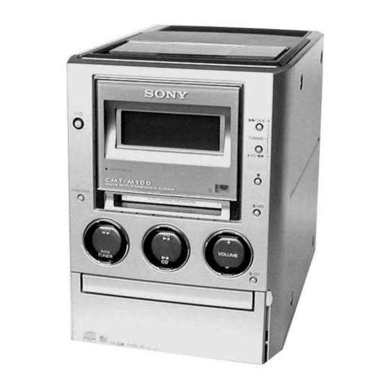
SERVICE MANUAL
Ver 1.0 2002. 02
HCD-M10 is the Amplifier, MD deck, CD
player, Tape player and Tuner section in
CMT-M100MD.
Amplifier section
European model:
DIN power output (Rated):10 +10 watts
(6 ohms at 1 kHz,DIN)
Continuous RMS power output (Reference):
15 +15 watts
(6 ohms at 1 kHz,10% THD)
Music power output (Reference):
25 +25 watts
Other models:
DIN power output (Rated):10 +10 watts
(6 ohms at 1 kHz,DIN)
Continuous RMS power output (Reference):
15 +15 watts
(6 ohms at 1 kHz,10% THD)
Inputs
ANALOG IN (phono jacks):
voltage 250 mV,
impedance 47 kilohms
Sony Corporation
9-873-570-01
Home Audio Company
2002B0200-1
Published by Sony Engineering Corporation
© 2002.02
HCD-M10
Model Name Using Similar Mechanism
CD
CD Mechanism Type
Section
Base Unit Type
Optical Pick-up Type
Model Name Using Similar Mechanism
MD
MD Mechanism Type
Section
Optical Pick-up Type
Tape deck
Model Name Using Similar Mechanism
Section
Tape Transport Mechanism Type
SPECIFICATIONS
DIGITAL OPTICAL IN (Supported sampling
frequencies:32 kHz,44.1 kHz and 48 kHz)
Outputs
PHONES (stereo minijack):
SPEAKER:
CD player section
System
Laser
Frequency response
MICRO HI-FI COMPONENT SYSTEM
AEP Model
UK Model
E Model
Australian Model
HCD-J300
CDM55A1-K4BD43
BU-K4BD43
KSM-213DHAP
HCD-C5
MDM-7B4M
KMS-260E
HCD-J300
Mech deck
accepts headphones of
16 ohms or more.
accepts impedance of 6 to
16 ohms.
Compact disc and digital
audio system
Semiconductor laser
(λ =780 nm)
Emission duration:
continuous
2 Hz – 20 kHz (±0.5 dB)
— Continued on next page —
Advertisement
Table of Contents


Need help?
Do you have a question about the HCD-M10 and is the answer not in the manual?
Questions and answers