Table of Contents
Advertisement
SERVICE MANUAL
Ver 1.1 2001. 10
• This set is the tuner, deck, CD
and amplifier section in MHC-MC1.
Manufactured under license from Dolby Laboratories
Licensing Corporation.
"DOLBY" and the double-D symbol a are trademarks
of Dolby Laboratories Licensing Corporation.
Amplifier section
U.S.A models:
AUDIO POWER SPECIFICATIONS
POWER OUTPUT AND TOTAL HARMONIC DISTORTION:
With 8 Ω loads both channels driven, from 70 – 20,000 Hz; rated 80 W per
channel minimum RMS power, with no more than 0.9% toral harmonic
distortion from 250 mW to read output.
Continuous RMS power output
80 + 80 W(8Ω at 1kHz, 10% THD)
Tortal harmonic distortion
less than 0.09%(8Ω at 1kHz, 40W)
Inputs
VIDEO/MD IN (phono jack):
voltage 250mV/450mV,
impedance 47kΩ
Outputs
VIDEO/MD OUT (phono jack):
voltage 250mV,
impedance 1kΩ
PHONES (stereo phone jacks):
accepts headphones of 8Ω or more
SPEAKER : accepts impedance of 8 to 16Ω
REAR SPEAKER :
accepts impedance of 16Ω
SUPER WOOFER :
Voltage 1V, impedance 1kΩ
CD player section
System
Compact disc and digital audio system
Laser
Semiconductor laser (λ =780mm)
Emission duration:
continuous
Sony Corporation
9-928-899-12
2001J1600-1
Home Audio Company
© 2001.10
Published by Sony Engineering Corporation
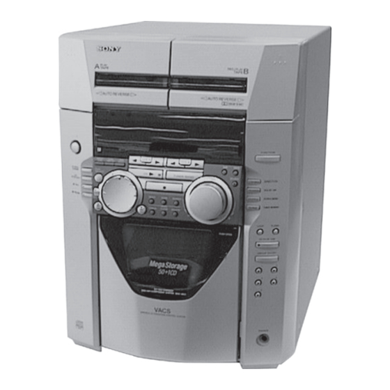
HCD-MC1
Model Name Using Similar Mechanism HCD-F150/FR10
CD
CD Mechanism Type
Section
Optical Pick-up Name
Model Name Using Similar Mechanism HCD-DR8AV
Tape deck
Section
Tape Transport Mechanism Type
SPECIFICATIONS
Laser output
Frequency response
Wavelength
Signal-to-noise retio
Dynamic range
CD OPTICAL DIGITAL OUT
(Square optical connector jack, rear panel)
Output Level
Tape player section
Recording system
Frequency response (DOLBY NR OFF)
Tuner section
FM stereo, FM/AM superheterodyne tuner
FM tuner section
Tuning range
Antenna
Antenna terminals
Intermediate frequency 10.7MHz
MINI HI-FI COMPONENT SYSTEM
US Model
E Model
CDM-46B1
KSS-213BA/F-NP
TCM-230AWR2/230PWR2
Max. 44.6µW*
*This output is the value measured at a distance of
200 mm from the objective lens surface on the
Optical Pick-up Block with 7 mm aperture.
2Hz – 20kHz (±0.5dB)
780 – 790nm
More than 90dB
More than 90dB
–18dBm
4-track 2-channel stereo
40 – 13,000Hz (±3dB),
using Sony TYPE I
cassette
40 – 14,000Hz (±3dB),
using Sony TYPE II
cassette
87.5 – 108.0MHz
FM lead antenna
75Ω unbalanced
— Continued on next page —
Advertisement
Table of Contents

Related Manuals for Sony HCD-MC1


Summary of Contents for Sony HCD-MC1
- Page 1 CD player section System Compact disc and digital audio system — Continued on next page — Laser Semiconductor laser (λ =780mm) Emission duration: continuous MINI HI-FI COMPONENT SYSTEM Sony Corporation 9-928-899-12 2001J1600-1 Home Audio Company © 2001.10 Published by Sony Engineering Corporation...
- Page 2 AM tuner section Tuning renge 530 – 1,710kHz (with the interval set at 10kHz) 531 – 1,710kHz (with the interval set at 9kHz) Antenna AM loop antenna Antenna terminals External antenna terminal Intermediate frequency 450kHz General Power requirements US model : 120V AC, 60Hz E model : 110 - 120V or 220 - 240V AC, 50/60Hz Power consumption...
-
Page 3: Leakage Test
COMPONENTS IDENTIFIED BY MARK ! OR DOTTED LINE WITH MARK ! ON THE SCHEMATIC DIAGRAMS AND IN THE PARTS LIST ARE CRITICAL TO SAFE OPERATION. REPLACE THESE COMPONENTS WITH SONY PARTS WHOSE PART NUMBERS APPEAR AS SHOWN IN THIS MANUAL OR IN SUPPLEMENTS PUBLISHED BY SONY. -
Page 4: Table Of Contents
SERVICING NOTES TABLE OF CONTENTS NOTES ON HANDLING THE OPTICAL PICK-UP 1. GENERAL BLOCK OR BASE UNIT FRONT PANEL ····································································· 5 The laser diode in the optical pick-up block may suffer electrostatic REAR PANEL ········································································ 6 break-down because of the potential difference generated by the charged electrostatic load, etc. -
Page 5: General
SECTION 1 GENERAL FRONT PANEL !¡ !™ !£ #§ !¢ #∞ !∞ #¢ !§ #£ !¶ !• !ª @º @¡ #™ @™ #¡ @£ #º @ª @• @¶ @§ @∞ @¢ 1 1/u button !ª LOOP button 2 DISPLAY/MEMO button @º... -
Page 6: Rear Panel
REAR PANEL 1 VIDEO/MD (AUDIO) jack 2 ANTENNA terminal 3 AC power cord 4 REAR SPEAKER terminal 5 SPEAKER terminal 6 CD DIGITAL OUT connector 7 SUPER WOOFER jack — 6 —... - Page 7 This section is extracted from instruction manual. — 7 —...
-
Page 8: Disassembly
SECTION 2 DISASSEMBLY • This set can be disassembled in the order shown below. Back panel Main board Power transformer (T901) Front panel Case (Page 10) (Page 10) (Page 11) section (Page 8) (Page 9) CD mechanism Base BD board, Optical chassis deck section... - Page 9 2-2. FRONT PANEL SECTION 7 Lug 6 Screws (BVTT 3 × 8) 2 Wire (flat type) (17 core) 1 Wire (flat type) (15 core) 9 Two claws 3 Wire (flat type) (15 core) 4 Connector CN108 5 Connector CN454 9 Two claws 8 Three screws (BVTP 3 ×...
- Page 10 2-4. BACK PANEL 5 Thirteen screws (BVTP 3 × 8) 1 Wire (flat type) (13 core) 3 Five screws 2 Connector (BVTP 3 × 8) 4 Cover 6 Remove the back panel to direction of the arrow. 2-5. MAIN BOARD 5 Two connectors 7 Remove the MAIN board to direction...
- Page 11 3 Four screws (BVTT 3 × 8) 2-6. POWER TRANSFORMER (T901) 1 Connector 4 Power transforme 2 Power cord 2-7. SUB CHASSIS 1 Two screws (BVTT 3 × 8) 3 Sub chassis 2 Three screws (BVTP 3 × 8) 2 Two screws (BVTP 3 ×...
- Page 12 2-8. CD MECHANISM DECK SECTION 8 Three screws 5 Two screws (BVTT 3 × 10) (BVTT 3 × 6) 7 Reinforcement 9 Base (LOADING) 6 Wire holder !¡ Screw !™ Base (CDM) (BVTT 3 × 10) 1 Screw (PTPWH 2.6 × 8) 3 Bwo screws 0 Screw (BVTP 3 ×...
- Page 13 2-10. BD BOARD, SLED MOTOR (M102) 6 Gear (A) (S) 8 Gear cover 5 Claw 7 Three claws !º Two screws (+P 2 × 2) 9 Gear (B) (RP) 1 Wire (flat type) (16 core) !¡ Sled motor (M102) 4 BD board 2 Screw (+PTPWH 2 ×...
- Page 14 2-12. TAPE MECHANISM DECK SECTION 2 Remove the cassette lid (L) ass'y to direction of the arrow B . 4 Remove the tape mechanism deck section. 3 Three screws (BVTP 3 × 6) 3 Three screws (BVTP 2.6 × 8) 1 Remove the cassette lid (R) ass'y to direction of the arrow A .
- Page 15 2-14. AUDIO BOARD 4 AUDIO board 3 Two screws 1 Four rivets (BTP 2.6 × 4) 2 Break the soldering of two flexible flat cables. 2-15. CAPSTAN MOTOR (M1) 4 Removal the capstan motor to direction of the arrow. 3 Hang the belt. 2 Hang the belt.
-
Page 16: Test Mode
1. Press the three buttons STOP , ENTER and GROUP 2 at the RAM to initial conditions. Execute this mode when returning same time. The HCD-MC1 enters the GC test mode, and all of the set to the customer. the fluorescent tubes and LEDs turn on. - Page 17 2. VOLUME Check Mode 5. The tape A is rewound and stops at the shut-off. The aging The maximum volume is set, and the VOLUME MAX display mode advances to the next step. and the GEQ display are displayed for a moment regardless of The message: TAPE A AG-5 appears.
-
Page 18: Mechanical Adjustments
SECTION 4 MECHANICAL ADJUSTMENTS • TAPE MECHANISM DECK SECTION • Torque Measurement Precaution Torque meter Meter reading Mode 1. Clean the following parts with a denatured alcohol-moistened 31 to 71 g • cm swab: CQ-102C (0.43 – 0.98 oz • inch) record/playback heads pinch rollers 2 to 6 g •... - Page 19 PLUS ONE 5. The disc table rotates in the clockwise direction. The disc table rotation time is displayed with ‘’PLUS ONE” slit as a measuring point. 6. Measure the waveform of the oscilloscope when the disc table is rotating. 7. Move the holder (sensor) center so that the flat portion center at the top of the D.SENS (CH1) input waveform and the ‘’H” center of HHOUT (CH2) coincide.
- Page 20 MAGNET ASSY ALIGNMENT 1. Check that there is no disc in the unit and then turn ON the power. Open the door, and set a disc in the PLUS ONE slit. 2. Close the door, and while pressing the button, ENTER button and GROUP 5 button simultaneously. 3.
-
Page 21: Electrical Adjustments
SECTION 5 ELECTRICAL ADJUSTMENTS 2. Turn the adjustment screw and check output peaks. If the peaks DECK SECTION 0 dB=0.775 V do not match for L-CH and R-CH, turn the adjustment screw so that outputs match within 1dB of peak. 1. - Page 22 DECK B Tape Speed Adjustment DECK B REC Bias Adjustment Note: Start the Tape Speed adjustment as below after setting to the test Procedure: mode. INTRODUCTION In the test mode, the tape speed is high during pressing the When set to the test mode performed in Tape Speed Adjustment, HI-SPEED DUBBING button.
- Page 23 4. Mode: Record MD/VIDEO (AUDIO) IN 315 Hz, 50 mV (–23.8 dB) AF OSC blank tape 600 Ω CS-123 attenuator 5. Mode: Playback recorded level meter portion – CN301 (Pin 3 : L-CH) (Pin 1 : R-CH) 6. Confirm playback the signal recorded in step 3 become adjustable level as follows.
-
Page 24: Cd Section
10. Confirm that oscilloscope waveform is clear and check RF signal CD SECTION level is correct or not. 11. Turn OFF the power, and remove the lead wire connected at Note : step 7. CD Block is basically designed to operate without adjustment. Therefore, check each item in order given. - Page 25 HCD-F150/FR10 Adjustment Location : oscilloscope BD board [ BD BOARD ] — CONDUCTOR SIDE — TP (TE) CN102 TP (VC) When a general remote commander is not used: Solder lead wires to TP (DVDD) and TP (TOFF) on the BD board severally.
-
Page 26: Diagrams
HCD-MC1 SECTION 6 DIAGRAMS 6-1. BLOCK DIAGRAMS CD SECTION OPTICAL PICK-UP BLOCK FOCUS/TRACKING/ (KSS-213BA/F-NP) SLED/SPINDLE SERVO DIGITAL SIGNAL RF AMP PROCESSOR A+5V IC402 DETECTOR IC101 IC102 • SIGNAL PATH A+5V RF SM EFMI D OUT DIGITAL D IN :DIGITAL OUT... - Page 27 HCD-MC1 MAIN SECTION R CH J781 PHONS R CH SOUND CONTROL TM701 J101 IC101 RY701 IN A L OUT POWER • RCH is omitted IN B (FRONT) Q111,112 Q113 IC801 Q801 Q811,812 Q701,702 • Signal Path R CH IN C...
- Page 28 HCD-MC1 AUDIO SECTION DECK PROCESS DECK A/B SELECT, PB/REC EQ AMP, DOLBY NR AMP, ALC, AMS • SIGNAL PATH IC301 : PLAYBACK (DECK A) DOLBY PASS HP101 (PLAYBACK) : PLAYBACK (DECK B) PB OUT (L) PB-L PB EQ AMP AIN (L)
-
Page 29: Circuit Boards Location
HCD-MC1 6-2. CIRCUIT BOARD LOCATION THIS NOTE IS COMMON FOR PRINTED WIRING BOARDS AND SCHEMATIC DIAGRAMS. TRANS board (In addition to this necessary note is printed in each POWER AMP board block.) For schematic diagrams. For printed wiring boards. Note:... -
Page 30: Printed Wiring Board Bd Section
HCD-MC1 6-3. PRINTED WIRING BOARD BD SECTION • See page 33 for Circuit Boards Location. • Semiconductor Location Ref. No. Location BD BOARD D151 IC101 IC102 M101 IC103 SPINDLE IC104 MOTOR Q101 Q102 Q103 (LIMIT) (VC) M102 SLED MOTOR (TE) -
Page 31: Schematic Diagram Bd Section
HCD-MC1 6-4. SCHEMATIC DIAGRAM BD SECTION • See page 71 for Waveforms. • See page 72 for IC Pin Functions. BA/F-NP 1SS133T The components identified by mark ! or dotted line with mark ! are critical for safety. Replace only with part number specified. - Page 32 HCD-MC1 6-5. PRINTED WIRING BOARD CD MOTOR SECTION • See Page 33 for Circuit Boards Location. MAIN BOARD CN461 (Page 52) TABLE SENSOR BOARD CD MOTOR BOARD TABLE MOTOR LOADING MOTOR (11) 1-663-974- MAIN BOARD 1-663-971- (11) CN453 (Page 52)
-
Page 33: Schematic Diagram Cd Motor Section
HCD-MC1 6-6. SCHEMATIC DIAGRAM CD MOTOR SECTION — 41 — — 42 —... -
Page 34: Printed Wiring Board Audio Section
HCD-MC1 6-7. PRINTED WIRING BOARD AUDIO SECTION • See page 33 for Circuit Boards Location. • Semiconductor Location Ref. No. Location IC601 E-12 IC602 IC611 Q621 Q622 Q623 (Page 51) MAIN BOARD CN106 — 43 — — 44 —... - Page 35 HCD-MC1 6-8. SCHEMATIC DIAGRAM AUDIO SECTION • See page 80 for IC Block Diagrams. MAIN BOARD CN106 (Page 55) 0.01 The components identified by mark ! or dotted line with mark ! are critical for safety. Replace only with part number specified.
-
Page 36: Printed Wiring Board Leaf Sw Section
HCD-MC1 6-9. PRINTED WIRING BOARD LEAF SW SECTION • See page 33 for Circuit Boards Location. MAIN BOARD CN107 • Semiconductor (Page 51) Location Ref. No. Location D1001 D1002 IC1001 IC1002 C-11 Q1001 — 47 — — 48 —... -
Page 37: Schematic Diagram Leaf Sw Section
HCD-MC1 6-10. SCHEMATIC DIAGRAM LEAF SW SECTION MAIN BOARD CN107 (Page 55) — 49 — — 50 —... - Page 38 HCD-MC1 6-11. PRINTED WIRING BOARD MAIN SECTION • See page 33 for Circuit Boards Location. • Semiconductor Location Ref. No. Location POWER AMP BOARD D141 C-10 NO801 X1: E MODEL MAIN BOARD D333 (Page 68) X2: US MODEL D401 I-10...
- Page 39 HCD-MC1 6-12. SCHEMATIC DIARGAM MAIN (1/5) SECTION EQUALIZER MICRO PROC. INTERFACE POWER AMP FM/AM TUNER UNIT IS SUPPLIED AS THE ASSEMBLED BLOCK (DECK A) — 53 — — 54 —...
- Page 40 HCD-MC1 6-13. SCHEMATIC DIARGAM MAIN (2/5) SECTION • See page 51 for Printed Wiring Board. • See page 71 for Waveforms. • See page 77 for IC Pin Functions. E MODEL 0.01µF BN1F4M 2SA115 BN1F4M BN1F4M PB (DECK A) ]: PB (DECK B) <...
- Page 41 HCD-MC1 6-14. SCHEMATIC DIARGAM MAIN (3/5) SECTION • See page 51 for Printed Wiring Board. • See page 71 for Waveforms. • See page 56 for IC Pin Functions. (CD DOOR) 0.33 0.01uF — 57 — — 58 —...
- Page 42 HCD-MC1 6-15. SCHEMATIC DIARGAM MAIN (4/5) SECTION • See page 51 for Printed Wiring Board. • See page 80 for IC Block Diagrams. POWER AMP BN1F4M BN1F4M 0.01uF 0.01uF The components identified by mark ! or dotted line with mark ! are critical for safety.
- Page 43 HCD-MC1 6-16. SCHEMATIC DIARGAM MAIN (5/5) SECTION • See page 51 for Printed Wiring Board. 2SB1375 BN1A4M 1375 2200 — 61 — — 62 —...
- Page 44 HCD-MC1 6-17. PRINTED WIRING BOARD PANEL SECTION • See page 33 for Circuit Boards Location. • Semiconductor Location PANEL BOARD Ref. No. Location D601 D602 D611 FL601 D612 E-10 D613 D614 C621 R623 D615 IC602 SW/POWER BOARD R624 D616 D-10...
-
Page 45: Schematic Diagram Panel Section
HCD-MC1 6-18. SCHEMATIC DIAGRAM PANEL SECTION • See page 80 for IC Block Diagrams. • See page 71 for Waveforms. • See page 79 for IC Pin Function Description. R652 — 65 — — 66 —... -
Page 46: Printed Wiring Board Power Section
HCD-MC1 6-19. PRINTED WIRING BOARD POWER SECTION • See page 33 for Circuit Boards Location. POWER AMP BOARD CN802 C818 C804 C801 R821 R813 IC801 Q801 C806 D821 C802 C811 D801 R812 C823 R802 C803 R809 D812 C857 D811 R823... -
Page 47: Schematic Diagram Power Section
HCD-MC1 6-20. SCHEMATIC DIAGRAM POWER SECTION US MODEL VOLTAGE CHANGE S991 E MODEL E MODEL 250V US MODEL US MODEL The components identified by mark ! or dotted line with mark ! are critical for safety. Replace only with part number specified. -
Page 48: Waveforms
HCD-MC1 6-21. WAVEFORMS 6-22. IC PIN FUNCTION DESCRIPTION – MAIN Section – – PANEL Section – BD BOARD IC101 LA9240M (FOCUS/TRACKING/SLED SERVO, RF AMP) Pin No. Pin Name Function IC601 8 (X-OUT) IC501 0 (X2) IC501 (¡ (CLK-OUT) Connected to the pick-up photodiode... - Page 49 Pin No. Pin Name Function SLOF Sled servo off control input CV– CLV error signal is input from the digital signal processor CLV error signal is input from the digital signal processor RFSM RF output Works together with the RFSM pin to set the RF gain and the 3T compensation constant for RFS–...
- Page 50 BD BOARD IC102 LC78622E (DIGITAL SIGNAL PROCESSOR) Pin No. Pin Name Function DEFI Defect detection signal (DEF) input (Be sure to connect to 0 when not in use) PLL test input to incorporates a pull-down resistor (Be sure to connect to 0V) PLL phase comparison output for external VCO control VVSS —...
- Page 51 Pin No. Pin Name Function EMPH Deemphasis monitor The deemphasis disc is being played back when “H” C2 flag output DOUT Digital OUT output (EIAJ format) TEST3 Test input Incorporates a pull-down resistor Be sure to connect to 0V TEST4 Test input Incorporates a pull-down resistor Be sure to connect to 0V —...
- Page 52 MAIN BOARD IC401 CXP84632-031Q (CD CHANGER CONTROL) Pin No. Pin Name Function — — Not used ICSW IC reset signal output — — Not used HHOUT Plus one LED signal output — — Not used 6 to 13 D0 to D7 SRAM data I/O 14 to 28 A0 to A14...
- Page 53 MAIN BOARD IC501 uPD780016AYGF-011-3BA (MAIN CONTROL) Pin No. Pin Name Function LINE-MUTE Line mute signal output DBFB-H/L DBFB H/L select signal output 442-LT Latch signal output for IC101(M62442FP) — — Not used POWER Power control signal output F-RELAY Main speaker relay control signal output R-RELAY Surround speaker relay control signal output(Not used) PL-RELAY...
- Page 54 Pin No. Pin Name Function Clock signal output for IC101(M62442FP) 442-CLK 442-DATA Data signal output for IC101(M62442FP) CENTER-MUTE Center speaker mute signal output Not used IIC-DATA Serial data output IIC-CLK Serial data clock output XRST CD reset signal output(Not used) CD latch signal output(Not used) FOCUS-SW Focus switching signal output(Not used)
- Page 55 PANEL BOARD IC601 TMP87CM74AF-6660 (DISPLAY CONTROL) Pin No. Pin Name Function 1 to 6 LED3 to LED8 LED driver output — Ground XOUT X’tal(5MHz) X’tal(5MHz) RESET Reset signal input 11,12 LED9,LED10 LED driver output TEST — Not used 14 to 18 LED11 to LED15 LED driver output 19,20...
-
Page 56: Ic Block Diagrams
6-23. IC BLOCK DIAGRAMS IC603 (PANEL BOARD) BA3833F-E2 IC461 (MAIN BOARD) BA6780 RESET RESET 18 RESET VIN1 VIN2 REFFERENCE PREF 17 f01 CURRENT FIN1 FIN2 LINE 16 f02 RIN1 RIN2 LINE 15 f03 IOUT BIAS 13 f VREF Bias 12 VCC FBIN- VREG 11 NC... -
Page 57: Exploded Views
SECTION 7 EXPLODED VIEWS NOTE: • -XX, -X mean standardized parts, so they may • The mechanical parts with no reference number The components identified by mark ! or have some differences from the original one. in the exploded views are not supplied. dotted line with mark ! are critical for safety. - Page 58 4-959-229-11 DETENT, CASSETTE 4-222-516-01 WINDOW (FL) 4-999-687-01 SPRING (B DECK) 4-989-312-01 LATCH, NS 4-222-488-01 LID(R), CASSETTE 4-222-487-01 WINDOW (CASSETTE) 4-962-708-71 EMBLEM (4-A), SONY 4-933-134-61 SCREW (+PTPWH M2.6 × 6) 4-222-536-01 LID(L), CASSETTE 4-999-686-01 SPRING (A DECK) 4-977-358-31 CUSHION 4-222-513-01 HOLDER (L), CASSETTE...
- Page 59 7-3. CHASSIS SECTION E MODEL US MODEL not supplied CD MECHANISM DECK SECTION-1 T991 supplied supplied CD MECHANISM DECK SECTION-2 supplied Ref. No. Part No. Description Remarks Ref. No. Part No. Description Remarks 4-988-439-01 HOLDER, TABLE 1-782-558-21 WIRE (FLAT TYPE) (16 CORE) 4-988-434-01 TABLE (50) 1-782-559-21 WIRE (FLAT TYPE) (9 CORE) 4-957-577-31 SCREW PTP WH (2.6 ×...
- Page 60 7-4. CD MECHANISM DECK SECTION-1 (CDM-46B1) OPTICAL PICK-UP SECTION not supplied Ref. No. Part No. Description Remarks Ref. No. Part No. Description Remarks * 301 1-663-975-11 DOOR SW BOARD * 315 4-988-421-01 HOLDER (MAGNET) * 302 4-988-427-01 COVER, CAM A-4672-522-A MAGNET ASSY 4-988-420-01 SLIDER (LOADING) * 319 4-976-473-01 HOLDER (LED-S)
- Page 61 7-5. CD MECHANISM DECK SECTION-2 (CDM-46B1) Ref. No. Part No. Description Remarks Ref. No. Part No. Description Remarks * 351 1-663-971-11 TABLE SENSOR BOARD * 357 4-988-426-01 BASE (CDM) 4-988-414-01 BELT * 358 1-663-972-11 DISC SENSOR (R) BOARD 4-988-423-01 GEAR (A) (LOADING) * 359 1-663-974-11 CDMOTOR BOARD 4-988-425-01 PULLEY...
- Page 62 7-6. OPTICAL PICK UP SECTION (KSS-213BA/F-NP) not supplied M102 M101 Ref. No. Part No. Description Remarks Ref. No. Part No. Description Remarks ! 401 8-848-379-31 DEVICE,OPTICAL KSS-213BA/F-NP * 405 A-4699-869-A BD BOARD,COMPLETE 2-626-907-01 GEAR(A)(S) * 406 4-992-054-01 RUBBER, VIBRATION PROOF 2-627-003-02 GEAR(B)(RP) 4-996-243-01 SCREW (M2), +PSW 2-626-908-01 SHAFT,SLED...
- Page 63 7-7. TAPE MECHANISM DECK SECTION-1 (TCM-230AWR2) (TCM-230PWR2) *NOTE: Two types of parts which are not interchangeable are available for the Head deck (A) ASSY and Head deck (B) ASSY. When replacing the parts, refer to the following figure, and use the appropriate part.
- Page 64 7-8. TAPE MECHANISM DECK SECTION-1 (TCM-230AWR2) (TCM-230PWR2) *NOTE: Two types of parts which are not interchangeable are available for the mechanical block assembly. When replacing the parts, refer to the following figure, and use the appropriate part. Parts with “P” mark: 230PWR2 Parts without “P”...
-
Page 65: Electrical Parts List
SECTION 8 AUDIO ELECTRICAL PARTS LIST NOTE: • Due to standardization, replacements in the • RESISTORS When indicating parts by reference number, parts list may be different from the parts All resistors are in ohms. please include the board name. specified in the diagrams or the components METAL: metal-film resistor used on the set. - Page 66 AUDIO Ref. No. Part No. Description Remarks Ref. No. Part No. Description Remarks < VARIABLE RESISTOR > C156 1-163-085-00 CERAMIC CHIP C157 1-164-232-11 CERAMIC CHIP 0.01uF RV301 1-238-598-11 RES, ADJ, CARBON 2.2K C158 1-163-038-91 CERAMIC CHIP 0.1uF RV311 1-238-598-11 RES, ADJ, CARBON 2.2K C159 1-163-101-00 CERAMIC CHIP 22PF...
- Page 67 CD DOOR CD LED CD MOTOR DISC SENSOR (R) Ref. No. Part No. Description Remarks Ref. No. Part No. Description Remarks < RESISTOR > R171 1-216-025-91 RES,CHIP 1/10W R172 1-216-025-91 RES,CHIP 1/10W R101 1-216-097-91 RES,CHIP 100K 1/10W R173 1-216-025-91 RES,CHIP 1/10W R102 1-216-093-00 METAL CHIP...
- Page 68 DISC SENSOR (S) DOOR LED DOOR SW FUNC HP/MIC LEAF SW Ref. No. Part No. Description Remarks Ref. No. Part No. Description Remarks 1-663-973-11 DISC SENSOR (S) BOARD R688 1-216-039-00 METAL CHIP 1/10W R689 1-216-041-00 METAL CHIP 1/10W ********************* R690 1-216-045-00 METAL CHIP 1/10W 4-976-473-01 HOLDER (LED-S)
- Page 69 LEAF SW MAIN Ref. No. Part No. Description Remarks Ref. No. Part No. Description Remarks < RESISTOR > C161 1-137-195-11 FILM 0.56uF C162 1-136-158-00 FILM 0.027uF R907 1-247-879-11 CARBON 100K 1/4W C163 1-136-167-00 FILM 0.15uF R1001 1-249-409-11 CARBON 1/4W F C164 1-130-480-00 MYLAR 0.0056uF 5%...
- Page 70 MAIN Ref. No. Part No. Description Remarks Ref. No. Part No. Description Remarks C405 1-162-306-11 CERAMIC 0.01uF C917 1-126-768-11 ELECT 2200uF C406 1-104-665-11 ELECT 100uF C918 1-126-968-11 ELECT 100uF C410 1-104-665-11 ELECT 100uF C919 1-126-968-11 ELECT 100uF C411 1-110-489-11 CAPACITOR 5.5V C921 1-126-947-11 ELECT...
- Page 71 MAIN Ref. No. Part No. Description Remarks Ref. No. Part No. Description Remarks D906 8-719-991-33 DIODE 1SS133T-77 Q163 8-729-141-30 TRANSISTOR 2SC3623ATP-LK D907 8-719-024-99 DIODE 11ES2-NTA2B Q191 8-729-141-30 TRANSISTOR 2SC3623ATP-LK D908 8-719-024-99 DIODE 11ES2-NTA2B Q331 8-729-116-59 TRANSISTOR 2SB1068TP D909 8-719-024-99 DIODE 11ES2-NTA2B Q332 8-729-029-66 TRANSISTOR DTC114ESA-TP D910...
- Page 72 MAIN Ref. No. Part No. Description Remarks Ref. No. Part No. Description Remarks R125 1-249-429-11 CARBON 1/4W R331 1-249-425-11 CARBON 4.7K 1/4W F R128 1-249-421-11 CARBON 2.2K 1/4W F R332 1-249-415-11 CARBON 1/4W F R131 1-247-807-31 CARBON 1/4W R333 1-249-421-11 CARBON 2.2K 1/4W F R132...
- Page 73 MAIN Ref. No. Part No. Description Remarks Ref. No. Part No. Description Remarks R524 1-249-429-11 CARBON 1/4W R740 1-249-429-11 CARBON 1/4W R526 1-249-429-11 CARBON 1/4W R741 1-249-429-11 CARBON 1/4W R531 1-247-807-31 CARBON 1/4W R742 1-249-429-11 CARBON 1/4W R532 1-247-807-31 CARBON 1/4W R751 1-247-791-91 CARBON...
- Page 74 PANEL Ref. No. Part No. Description Remarks Ref. No. Part No. Description Remarks A-4426-595-A PANEL BOARD, COMPLETE D628 8-719-074-81 DIODE MAA3864X-J300K (SELECTOR) D630 8-719-074-83 DIODE MPG3864X-J300K (TAPE B 9) ********************** D631 8-719-074-83 DIODE MPG3864X-J300K (TAPE B () 4-222-479-01 HOLDER, FL TUBE D632 8-719-074-83 DIODE MPG3864X-J300K (CD P) 4-222-480-01 SHEET (FL FILTER)
- Page 75 PANEL POWER AMP Ref. No. Part No. Description Remarks Ref. No. Part No. Description Remarks R625 1-216-089-91 RES,CHIP 1/10W S616 1-762-875-21 SWITCH, KEYBOARD(),+) R626 1-216-033-00 METAL CHIP 1/10W S617 1-762-875-21 SWITCH, KEYBOARD(TAPE B 9) R627 1-216-089-91 RES,CHIP 1/10W S618 1-762-875-21 SWITCH, KEYBOARD(TAPE B () R628 1-216-033-00 METAL CHIP 1/10W...
- Page 76 POWER AMP SW/POWER TABLE SENSOR TRANS Ref. No. Part No. Description Remarks Ref. No. Part No. Description Remarks < TRANSISTOR > R659 1-216-041-00 METAL CHIP 1/10W Q801 8-729-140-84 TRANSISTOR 2SC1841TP-PAFAEA < SWITCH > Q811 8-729-900-36 TRANSISTOR BA1F4M-TP Q812 8-729-620-05 TRANSISTOR 2SC2603TP-EF S625 1-762-875-21 SWITCH, KEYBOARD (POWER) Q851...
- Page 77 Ref. No. Part No. Description Remarks Ref. No. Part No. Description Remarks *************** MISCELLANEOUS *************** 1-693-457-11 ENCAPSULATED COMPONENT(TUNER UNIT) 1-769-972-11 WIRE(FLAT TYPE)(13 CORE) 1-773-004-11 WIRE(FLAT TYPE)(15 CORE) 1-765-332-11 WIRE (FLAT TYPE) (15 CORE) 1-773-055-11 WIRE (FLAT TYPE) (17 CORE) 1-769-920-11 WIRE (FLAT TYPE) (9 CORE) ! 109 1-569-007-21 ADAPTOR, CONVERSION 2P (E) 1-782-558-21 WIRE (FLAT TYPE) (16 CORE)
- Page 78 HCD-MC1 MEMO — 102 —...
- Page 79 HCD-MC1 US Model E Model SERVICE MANUAL CORRECTION-1 Correct your service manual as shown below. PARTS CHANGED : indicates correct portion Page INCORRECT CORRECT Ref. No. Part No. Description Ref. No. Part No. Description 4-222-508-01 PLATE(CD DOOR) 4-222-510-11 PLATE(CD DOOR)
- Page 80 HCD-MC1 REVISION HISTORY Clicking the version allows you to jump to the revised page. Also, clicking the version at the upper right on the revised page allows you to jump to the next revised page. Ver. Date Description of Revision 2001.10...
Need help?
Do you have a question about the HCD-MC1 and is the answer not in the manual?
Questions and answers
I was given this CD player and I don’t have the operating manual. I need it to make it work properly. The sound is beautiful
You can obtain the operating manual for the Sony HCD-MC1 CD player by purchasing a printed copy from the True Manuals website.
This answer is automatically generated