Table of Contents
Advertisement
Quick Links
Advertisement
Table of Contents

Subscribe to Our Youtube Channel
Related Manuals for Terasic DE10-Standard

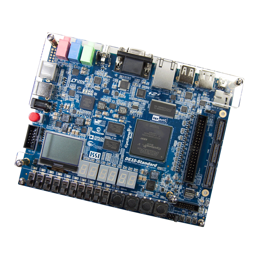
Summary of Contents for Terasic DE10-Standard
-
Page 2: Table Of Contents
Compile and Verify Your Design Chapter 4 4.1 Compile Your Design .............. 39 4.2 Program the FPGA Device ............41 4.3 Verify The Hardware ............... 45 Appendix Chapter 5 5.1 Headquarter & Branches ............48 DE10-Standard My First FPGA www.terasic.com February 15, 2017... -
Page 3: Introduction
This tutorial provides comprehensive information that will help you understand how to create a FPGA design and run it on your DE10-Standard development board. The following sections provide a quick overview of the design flow, explain what you need to get started, and describe what you will learn. -
Page 4: Before You Begin
Use the USB cable to connect the leftmost USB connector on the DE10-Standard board to a USB port on a computer that runs the Quartus II software. Turn on the power switch on the DE10-Standard board. - Page 5 Figure 1-3 Driver Software Installation Since the desired driver is not available on the Windows Update Web site, open the Computer Management and select the Device Manager. This leads to the window in Figure 1-4. DE10-Standard My First FPGA www.terasic.com February 15, 2017...
- Page 6 Right click Other devices>Unknown device and select Update Driver Software…This leads to the window in Figure 1-5 Figure 1-5 Update Driver Software The driver is available within the Quartus II software. Hence, click Browse my computer for device software to get to DE10-Standard My First FPGA www.terasic.com February 15, 2017...
- Page 7 Figure 1-6. Click Next. Figure 1-7 Browse to find the location The driver will now be installed as indicated in Figure 1-8 Click close and you can start using the DE10-Standard board. DE10-Standard My First FPGA www.terasic.com February 15, 2017...
-
Page 8: What You Will Learn
Of course, you can use your DE10-Standard board to run other designs as well. For the LED design, you will write Verilog HDL code for a simple 32-bit counter, add a phase-locked loop (PLL) megafunction as the clock source, and add a 2-input multiplexer megafunction. -
Page 9: Assign The Device
1. In the Quartus II software, select File > New Project Wizard. The Introduction page opens. See Figure 2-1. Figure 2-1 New Project Wizard introduction DE10-Standard My First FPGA www.terasic.com February 15, 2017... - Page 10 What is the name of this project? Type my_first_fpga. e. What is the name of the top-level design entity for this project? Type my_first_fpga. See Figure 2-2. Figure 2-2 Project information f. Click Next thrice. DE10-Standard My First FPGA www.terasic.com February 15, 2017...
- Page 11 2-3. Figure 2-3 Specify the Device Example h. Click Finish. When prompted, choose Yes to create the my_first_fpga project directory. You just created your first Quartus II FPGA project. See Figure 2-4. DE10-Standard My First FPGA www.terasic.com February 15, 2017...
- Page 12 Figure 2-4 my_first_fpga project DE10-Standard My First FPGA www.terasic.com February 15, 2017...
-
Page 13: Design Entry
When creating your own designs, you can choose any of these methods or a combination of them. Choose File > New > Block Diagram/Schematic File (see to create a new file, Figure 3-1 Block1.bdf, which you will save as the top-level design. DE10-Standard My First FPGA www.terasic.com February 15, 2017... - Page 14 Choose File > Save As and enter the following information. File name: my_first_fpga Save as type: Block Diagram/Schematic File (*.bdf) Click Save. The new design file appears in the Block Editor (see Figure 3-2). DE10-Standard My First FPGA www.terasic.com February 15, 2017...
- Page 15 Click OK to create a new file Verilog1.v, which you will save as simple_counter.v. Select File > Save As and enter the following information (see Figure 3-3). File name: simple_counter.v Save as type: Verilog HDL File (*.v, *.vlg, *.verilog) DE10-Standard My First FPGA www.terasic.com February 15, 2017...
- Page 16 //It has a single clock input and a 32-bit output port module simple_counter ( CLOCK_50, counter_out input CLOCK_50 ; output [31:0] counter_out; [31:0] counter_out; always @ (posedge CLOCK_50) // on positive clock edge begin DE10-Standard My First FPGA www.terasic.com February 15, 2017...
- Page 17 10. The Quartus II software creates a Symbol File and displays a message (see Figure 3-5). Figure 3-5 Create Symbol File was Successful 11. Right click > Open Symble file to see the simple_counter.v symbol DE10-Standard My First FPGA www.terasic.com February 15, 2017...
- Page 18 BDF. You can move the block after placing it by simply clicking and dragging it to where you want it and releasing the mouse button to place it. See Figure 3-7. DE10-Standard My First FPGA www.terasic.com...
- Page 19 This tutorial design uses a PLL clock source to drive a simple counter. A PLL uses the on-board oscillator (DE10-Standard Board is 50 MHz) to create a constant clock frequency as the input to the counter. To create the clock source, you will add a pre-built IP core named Altera PLL.
- Page 20 Under What name do you want for the output file? Type pll.v at the end of the already created directory name. Click Next. Figure 3-9 Save IP Variation In the MegaCore Manager window, make the following selections (see Figure 3-10). DE10-Standard My First FPGA www.terasic.com February 15, 2017...
- Page 21 The device speed grade choose 6 for DE10-Standard. Set the frequency of the refclk input 50 MHz. Figure 3-10 MegaWizard Plug-In Manager Selections Turn off the Enable locked output port option on MegaCore. As you turn it off, pin disappears from the PLL block’s graphical preview.
- Page 22 Figure 3-11 MegaWizard Plug-In Manager Selections Then, make the following selection (see Figure 3-12). Desired Frequency input 5.0 Figure 3-12 MegaWizard Plug-In Manager Selections 8. Click Finish . It leads to Figure 3-13.Click Exit. DE10-Standard My First FPGA www.terasic.com February 15, 2017...
- Page 23 11. Click OK and place the pll symbol onto the BDF to the left of the simple_counter symbol. You can move the symbols around by holding down the left mouse button, helping you ensure that they line up properly. See Figure 3-15. DE10-Standard My First FPGA www.terasic.com February 15, 2017...
- Page 24 Figure 3-16 Draw a Bus Line connect pll outclk_0 port to simple_counter CLOCK_50 port Add an input pin and an output bus with the following steps: Right click> Insert >Symbol…. Under Libraries, select quartus/libraries > primitives > pin >input. See Figure 3-17. DE10-Standard My First FPGA www.terasic.com February 15, 2017...
- Page 25 Change the pin name by double-clicking pin_name and typing CLOCK_50 (see Figure 3-19). This name correlates to the oscillator clock that is connected to the FPGA. Using the Orthogonal Bus tool, draw a bus line connected on one side to the simple_counter DE10-Standard My First FPGA www.terasic.com February 15, 2017...
- Page 26 BDF schematics, where X is the most significant bit (MSB) and Y is the least significant bit (LSB). Click OK. Figure 3-21 shows the BDF. DE10-Standard My First FPGA www.terasic.com February 15, 2017...
- Page 27 Figure 3-20 Change the output BUS name DE10-Standard My First FPGA www.terasic.com February 15, 2017...
-
Page 28: Add A Multiplexer
This design uses a multiplexer to route the simple_counter output to the LED pins on the DE10-Standard development board. You will use the MegaWizard Plug-In Manager to add the multiplexer, lpm_mux. The design multiplexes two variations of the counter bus to four LEDs on the DE10-Standard development board. - Page 29 Choose Verilog HDL as the output file type, and name the output file counter_bus_mux.v (see Figure 3-22. Figure 3-22 Save lpm_mux Variation Click OK. The MegaWizard Plug-in Manage window pops up. DE10-Standard My First FPGA www.terasic.com February 15, 2017...
- Page 30 Under How ‘wide’ should the data input and result output be? Select 4 (see Figure 3-23). Figure 3-23 lpm_mux settings Click Next. Click Finish twice. The Symbol window appears (see Figure 3-24 for an example) when you right click and select Insert > Symbol. DE10-Standard My First FPGA www.terasic.com February 15, 2017...
- Page 31 Figure 3-25 Place the lpm_mux symbol 13. Add input buses and output pins to the counter_bus_mux symbol as follows: Using the Orthogonal Bus tool, draw bus lines from the data1x[3..0] and data0x[3..0] DE10-Standard My First FPGA www.terasic.com February 15, 2017...
- Page 32 If you have not done so already, save your project file before continuing. 14. Right click on the mouse and select Insert > Symbol 15. Under Libraries, double-click quartus/libraries/ > primitives > pin > output (see Figure 3-27). DE10-Standard My First FPGA www.terasic.com February 15, 2017...
- Page 33 19. Attach an input pin to the multiplexer select line using an input pin: Right click on the mouse and select Insert > Symbol. Under Libraries, double-click quartus/libraries/ > primitives > pin > input. Click OK. DE10-Standard My First FPGA www.terasic.com February 15, 2017...
- Page 34 25. Under Libraries, double-click quartus/libraries/ > primitives >logic > not (see Figure 3-30). 26. Click OK. 27. Place this not pin so that it connects to KEY[1] and the pll rst (see Figure 3-31 Figure 3-29 Adding the KEY [1:0] Input Pin DE10-Standard My First FPGA www.terasic.com February 15, 2017...
- Page 35 Text tool on the toolbar (indicated with the A symbol). For example, you can add the label “OFF = SLOW, ON = FAST” to the KEY [0] input pin and add a project description, such as “My First FPGA Project.” DE10-Standard My First FPGA www.terasic.com February 15, 2017...
-
Page 36: Assign The Pins
Choose Assignments > Pin Planner, which opens the Pin Planner, a spreadsheet-like table of specific pin assignments. The Pin Planner shows the design’s six pins. See Figure 3-32. DE10-Standard My First FPGA www.terasic.com February 15, 2017... - Page 37 Figure 3-32 Pin Planner Example In the Location column next to each of the seven node names, add the coordinates (pin numbers) as shown in Table 3-1 for the actual values to use with your DE10-Standard board. Table 3-1 Pin Information Setting...
-
Page 38: Create A Default Timequest Sdc File
Synopsys Design Constraints File (.sdc) that the Quartus II TimeQuest Timing Analyzer uses during design compilation. For more complex designs, you will need to consider the timing requirements more carefully. To create an SDC, perform the following steps: DE10-Standard My First FPGA www.terasic.com February 15, 2017... - Page 39 Naming the SDC with the same name as the top-level file except for the .sdc extension causes the Quartus II software to using this timing analysis file automatically by default. If you used another name, you would need to add the SDC to the assignments file list. DE10-Standard My First FPGA www.terasic.com February 15, 2017...
- Page 40 DE10-Standard My First FPGA www.terasic.com February 15, 2017...
-
Page 41: Compile And Verify Your Design
In the Processing menu, choose Start Compilation or click the Play button on the toolbar. If you are asked to save changes to your BDF, click Yes. While compiling your design, the Quartus II software provides useful information about the compilation (see Figure 4-1). DE10-Standard My First FPGA www.terasic.com February 15, 2017... - Page 42 I/O pins used for the LEDs were not set. The software provides the compilation results in the Compilation Report tab as shown in Figure 4-2. DE10-Standard My First FPGA www.terasic.com February 15, 2017...
-
Page 43: Program The Fpga Device
Connect the power supply cable to your board and to a power outlet. For the DE10-Standard board, connect the USB-BlasterII (included in your development kit) to J13 and the USB cable to the USB-BlasterII. Connect the other end of the USB cable to the host computer. - Page 44 Figure 4-3 Programmer Window 2. Click Hardware Setup. 3. If it is not already turned on, turn on the DE10-Standard [USB-1] option under currently selected hardware. See Figure 4-4. DE10-Standard My First FPGA www.terasic.com February 15, 2017...
- Page 45 Figure 4-4 Hardware Setting 4. Click Close. 5. Click Auto Detect to detect all the devices on the JTAG chain. 6. Select 5CSXFC6D6 and click OK. DE10-Standard My First FPGA www.terasic.com February 15, 2017...
- Page 46 Figure 4-5 Select FPGA Device 7. Both HPS and FPGA will be list on the programmer. Select FPGA device and click Change File a .sof file. Figure 4-6 Programmer window DE10-Standard My First FPGA www.terasic.com February 15, 2017...
-
Page 47: Verify The Hardware
Press and hold KEY [0] on the development board and observe that the LEDs advance more quickly. Pressing this KEY causes the design to multiplex using the faster advancing part of the DE10-Standard My First FPGA www.terasic.com February 15, 2017... - Page 48 If other LEDs emit faintness light, Choose Assignments > Device. Click Device and Pin Options. See Figure 4-8. Figure 4-8 Device and Options Choose unused pins. Reserve all unused pins: Choose the As input tri-stated option. See Figure 4-9. DE10-Standard My First FPGA www.terasic.com February 15, 2017...
- Page 49 In the Processing menu, choose Start Compilation. After the compile, Choose Tools > Programmer. Select the my_first_fpga.sof file from the project directory. Click Start. At this time you could find the other LEDs are unlighted. DE10-Standard My First FPGA www.terasic.com February 15, 2017...
-
Page 50: Appendix
Chapter 5 Appendix & & Tel :+886-3-575-0880 Fax :+886-3-572-6690 Add:9F, No.176, Sec.2, Gongdao 5th Rd, East Dist, Hsinchu City, Taiwan 300-70 Email:sales@terasic.com / support@terasic.com DE10-Standard My First FPGA www.terasic.com February 15, 2017...
Need help?
Do you have a question about the DE10-Standard and is the answer not in the manual?
Questions and answers