Table of Contents
Advertisement
Quick Links
Advertisement
Table of Contents

Related Manuals for Advantech PCI-1742U


Summary of Contents for Advantech PCI-1742U
- Page 1 PCI-1742U 16-bit, 1MS/s High-Resolution Multifunction Card User Manual...
- Page 2 No part of this man- ual may be reproduced, copied, translated or transmitted in any form or by any means without the prior written permission of Advantech Co., Ltd. Information provided in this manual is intended to be accurate and reli- able.
- Page 3 Product Warranty (2 years) Advantech warrants to you, the original purchaser, that each of its prod- ucts will be free from defects in materials and workmanship for two years from the date of purchase. This warranty does not apply to any products which have been repaired or...
-
Page 4: Packing List
Step 1. Visit the Advantech web site at www.advantech.com/support where you can find the latest information about the product. Step 2. Contact your distributor, sales representative, or Advantech's cus- tomer service center for technical support if you need additional assistance. Please have the following information ready:... -
Page 5: Table Of Contents
Contents Chapter 1 Introduction ............. 2 Introduction ............... 2 Features ................2 1.2.1 Auto-Calibration Function ..........2 1.2.2 BoardID ................. 3 1.2.3 Plug-and-Play Function ..........3 1.2.4 Onboard FIFO Memory ..........3 1.2.5 Onboard Programmable Timer/Counter ......3 Installation Guide .............. 4 Figure 1.1:Installation Flow Chart ......... - Page 6 Digital Input /Output: ............42 Counter/Timer: ..............42 General ................42 Appendix B Block Diagram ..........44 Appendix C 82C54 Counter Chip Function..... 46 Intel 82C54..............46 Counter Read/Write & Control Registers ....... 47 Counter Operating Modes ..........50 PCI-1742U User Manual...
- Page 7 Introduction This chapter introduces PCI-1742U and shows how to install the software and information on useful accessories. Sections include: • Introduction • Features • Installation Guide • Software • Accessories...
-
Page 8: Chapter 1 Introduction
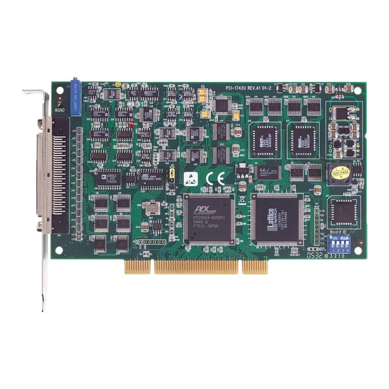
Chapter 1 Introduction 1.1 Introduction Thank you for buying the Advantech PCI-1742U PCI card. PCI-1742U is a powerful high-resolution multifunction DAS card with 1MS/s sampling rate and 16-bit resolution, fulfills the needs of most data acquisition appli- cations. PCI-1742U provides 16 single-ended or 8 differential analog input channels, two 16-bit D/A output channels, 16 digital input/output channels, and one 10 MHz 16-bit counter channel. -
Page 9: Boardid
1.2.2 BoardID The PCI-1742U has a built-in DIP switch that helps define each card’s unique ID when multiple PCI-1742U cards have been installed on the same PC chassis. The BoardID setting function is very useful when build- ing a system with multiple PCI-1742U cards. With the correct BoardID settings, you can easily identify and access each card during hardware configuration and software programming. -
Page 10: Installation Guide
1.3 Installation Guide Before you install your PCI-1742U card, please make sure you have the following necessary components: • PCI-1742U Multifunction Card • PCI-1742U User Manual • Driver software Advantech DLL Drivers (in the companion CD-ROM) • Computer: PC with a PCI-bus slot running Windows 2000/XP •... -
Page 11: Figure 1.1:Installation Flow Chart
Figure 1.1: Installation Flow Chart 1.4 Software Advantech offers a rich set of DLL drivers, 3rd-party driver support and application software to help fully exploit the functions of your PCI-1742U card: • DLL driver (on the companion CD-ROM) • LabVIEW driver •... -
Page 12: Accessories
For more information, please refer to Appendix C, Register Structure & Format. 1.5 Accessories Advantech offers a complete set of accessory products to support the PCI- 1742U cards. These accessories include: 1.5.1 PCL-10168 Wiring Cable The PCL-10168 shielded cable is specially designed for PCI-1742U cards to provide high resistance to noise. - Page 13 Installation This chapter provides a packaged item checklist, proper instructions about unpacking and step-by-step procedures for both driver and card installation. Sections include: • Unpacking • Driver Installation • Hardware Installation • Device Configuration & Testing • Device Testing...
-
Page 14: Chapter 2 Installation
Chapter 2 Installation 2.1 Unpacking After receiving your PCI-1742U package, please inspect its contents first. The package should contain the following items: • PCI-1742U card • Companion CD-ROM (DLL driver included) • User Manual The PCI-1742U card harbors certain electronic components vulnerable to electrostatic discharge (ESD). -
Page 15: Driver Installation
We recommend installing the driver before you plug the PCI-1742U Card into your system, since this will guarantee a smooth installation process. The 32-bit DLL driver Setup program for the PCI-1742U card is included on the companion CD-ROM that is shipped with your DAS card package. -
Page 16: Figure 2.2:Driver Setup
Figure 2.2: Driver Setup For further information on driver-related issues, an online version of the DLL Drivers Manual is available by accessing the following path: Start/ Programs/ Advantech Automation/ Device Manager/ Device Driver's Manual. PCI-1742U User Manual... -
Page 17: Hardware Installation
Step 4: Touch the metal part on the surface of your computer to neutralize any static electricity that might be in your body. Step 5: Insert the PCI-1742U card into a PCI slot. Hold the card only by its edges and carefully align it with the slot. Insert the card firmly into place. -
Page 18: Figure 2.3:Device Manager
After the PCI-1742U card is installed, you can verify whether it is prop- erly installed on your system in the Device Manager: Access the Device Manager through Start/ Control Panel/ System/ Device Manager. The device name of PCI-1742U should be listed on the Device Manager. -
Page 19: Device Configuration & Testing
The Device Manager program is a utility that allows you to configure and test your device, and later stores your settings on the system registry. These settings will be used when you call the APIs of Advantech Device Drivers. After properly installing PCI-1742U, you can now proceed to configure and test the device by clicking the Setup/Test button on the I/O Device Manager dialog box. -
Page 20: Figure 2.5:The Device Setting Dialog Box
Device Configuration In the Device Setting dialog box (Figure2.5), you can configure the A/D channel as Single-ended or Differential and choose the D/A channel ref- erence voltage source type. Figure 2.5: The Device Setting Dialog Box PCI-1742U User Manual... -
Page 21: Device Testing
Note: You can access the Device Test dialog box through the previous procedure for the Device Installation, or simply by accessing Start/Programs/Advantech Automation/ Device Manager/Advantech Device Manager. All functions are performed by the software polling method. For high speed data acquirements or output, functions have to use a corresponding VC example like ADINT or ADBMDMA. -
Page 22: Figure 2.6:Analog Input Tab
Click the Analog Output tab to bring it up to the foreground. The Analog Output tab allows you to output quasi-sine, triangle, or square waveforms automatically, or output single values manually. You can also configure the waveform frequency and output voltage range. Figure 2.7: Analog Output Tab PCI-1742U User Manual... -
Page 23: Testing Digital Input Function
2.5.3 Testing Digital Input Function Click the Digital Input tab to show forth the Digital Input test panel as seen below. Through the color of the lamps, you can easily discern whether the status of each digital input channel is high or low. Figure 2.8: Digital Input Tab 2.5.4 Testing Digital Output Function Click the Digital Output tab to bring up the Digital Output test panel such... -
Page 24: Testing Counter Function
Only after your card device is properly set up, configured and tested, can the device installation procedure be counted as complete. After the device installation procedure is completed, you can safely proceed to the next chapter, Signal Connections. PCI-1742U User Manual... - Page 25 Signal Connections This chapter provides useful informa- tion about how to connect input and output signals to PCI-1742U via the I/O connector. Sections include: • I/O Connector • Analog Input Connections • Analog Output Connections • Trigger Source Connections • Field Wiring Considerations...
-
Page 26: Chapter 3 Signal Connections
Chapter 3 Signal Connections 3.1 I/O Connector The I/O connector on the PCI-1742U is a 68-pin connector that enables you to connect to accessories with the PCL-10168 shielded cable. Fig. 3-1 shows the pin assignments for the 68-pin I/O connector on the PCI-1742U, and table 3-1 shows the I/O connector signal description. - Page 27 Table 3.1: I/O Connector Signal Description CNT0_CLK DGND Input Counter 0 Clock Input. The clock input of counter 0 can be either external or inter- nal , as set by software. CNT0_OUT DGND Output Counter 0 Output. CNT0_GATE DGND Input Counter 0 Gate Control.
-
Page 28: Pin Assignment
3.1.2 Pin Assignment Figure 3.1: I/O Connector Pin Assignments PCI-1742U User Manual... -
Page 29: Analog Input Connections
A signal source without a local ground is also called a “floating source”. It is fairly simple to connect a single-ended channel to a floating signal source. In this mode, the PCI-1742U provides a reference ground for external floating signal sources. Fig. 3-2 shows a single-ended channel connection between a floating signal source and an input channel on PCI- 1742U. -
Page 30: Differential Channel Connections
Low input. Figure 3-3 shows a differential channel connection between a ground-reference signal source and an input channel on the PCI-1742U. With this connection, the PGIA rejects a common-mode voltage V between the signal source and the PCI-1742U ground, shown as V in Figure 3-3. -
Page 31: Figure 3.4:Differential Connection - Floating Signal
Figure 3.4 shows a differential channel connection between a floating signal source and an input channel on PCI-1742U. In this figure, each side of the floating signal source is connected through a resistor to the AIGND. This connection can reject the common-mode voltage between the signal source and the PCI-1742U ground. -
Page 32: Analog Output Connections
32-bit timer for pacer triggering. A low-to-high edge from the Counter 2 output (PACER_OUT) will trigger an A/D conversion on the PCI-1742U. At the same time, you can also use this signal as a synchro- nous signal for other applications. -
Page 33: External Trigger Source Connection
3.5 Field Wiring Considerations When you use the PCI-1742U to acquire data from outside, noises in the environment might significantly affect the accuracy of your measure- ments if due cautions are not taken. The following measures will be help- ful to reduce possible interference running signal wires between signal sources and the PCI-1742U. -
Page 34: Boardid Switch Settings
PCI-1742U: Figure 3.7: Jumpers and Switch Locations The PCI-1742U has a built-in DIP-switch (SW1), which is used to define each the BoardID. You can determine the BoardID switch on the register. When there are multiple cards on the same chassis, this BoardID switch setting function is useful for identifying each card device number through BoardID switch. -
Page 35: Table 3.2:Boardid Setting
Table 3.2: BoardID Setting ID3* Board ID Note: On: 1, Off: 0 *ID3: the most significant bit (MSB) of BoardID Chapter 3... - Page 36 PCI-1742U User Manual...
- Page 37 Software Overview This chapter gives you an overview of the software programming choices available and a quick reference of source codes. Sections include: • Software Overview • Programming Choices • DLL Driver Programming...
-
Page 38: Chapter 4 Software Overview
4.2.1 DLL Driver The Advantech DLL Drivers software is included on the companion CD- ROM at no extra charge. It also comes with all the Advantech DAS cards. Advantech’s DLL driver features a complete I/O function library to help boost your application performance. The Advantech DLL driver for Win- dows 2000/XP works seamlessly with development tools such as Visual C++, Visual Basic, Borland C++ Builder and Borland Delphi. -
Page 39: Programming Tools
Driver and the Function Overview chapters in the DLL Drivers Manual. 4.3.2 Programming with DLL Driver Function Library Advantech DLL driver offers a rich function library to be utilized in vari- ous application programs. This function library consists of numerous APIs that support many development tools, such as Visual C++, Visual Basic, Delphi and C++ Builder. -
Page 40: Troubleshooting Dll Driver Error
DRV_GetErrorMessage function to return the error message. Or you can refer to the DLL Driver Error Codes Appendix in the DLL Drivers Manual for a detailed listing of the Error Code, Error ID and the Error Message. PCI-1742U User Manual... - Page 41 Calibration This chapter provides brief information on PCI-1742U calibration. Sections include: • VR Assignment...
-
Page 42: Chapter 5 Calibration
DAS card is stable. 5.1 VR Assignment There is one variable resistor (VR1) on the PCI-1742U to adjust the accu- rate reference voltage on the PCI-1742U. We provide a test point (See TP3 in Figure 5.1) for you to check the reference voltage on board. -
Page 43: Calibration Utility
5.1.1 Calibration Utility Users can access the "AD and DA Auto Calibration" utility through the Advantech Device Manger Figure 5.2: AD and DA Auto Calibration Utility Please follow the utility instructions to complete AD/DA calibration. Chapter 5... -
Page 44: Figure 5.3:Calibration Utility Instruction
Figure 5.3: Calibration Utility Instruction Item 1: AD calibration steps; Item 2: DA calibration steps; Item 3: Show AD/DA calibration parameters and status. PCI-1742U User Manual... - Page 45 Specifications...
-
Page 46: A.1 Analog Input
Impedance DC DNLE: ±1LSB Accuracy INLE: ±3LSB Offset error: Adjustable to ±2 LSB Gain Gain error 0.02 0.02 0.02 0.03 0.04 (% FSR) AC THD: -90 dB ENOB: 13.5 bits @ 1MS/s 14.5 bits @ < 250KS/s PCI-1742U User Manual... -
Page 47: Analog Output
A.2 Analog Output: Channels 16-bit Resolution 2MS/s max. per channel (FSR) Throughput Using Internal 0~+5V, 0~+10 V, -5~+5V,- Output Range Reference 10~+10V (Internal & External Reference) Using External 0~+x V@ +x V (-10 x 10) Reference -x~+x V@ +x V (-10 x 10) DNLE: ±1LSB (monotonic) Accuracy INLE: ±2LSB... -
Page 48: Digital Input /Output
Power Consumption +12 V @ 600 mA Max. +5 V @ 1 A Operation 0~+60°C (32~158°F) Temperature (refer to IEC 68-2-1,2) Storage -20~+85°C (-4~185°F) 5 ~ 95% RH non-condensing Relative Humidity (refer to IEC 68-2-3) CE certified Certification PCI-1742U User Manual... - Page 49 Block Diagram...
-
Page 50: Appendix B Block Diagram
Appendix B Block Diagram PCI-1742U User Manual... - Page 51 82C54 Counter Chip Function...
-
Page 52: Appendix C 82C54 Counter Chip Function
Counter 0 On the PCI-1742U, counter 0 can be a 16-bit timer or an event counter as chosen by the user. When the clock source is set as an internal source, counter 0 is a 16-bit timer. -
Page 53: Counter Read/Write & Control Registers
C.2 Counter Read/Write & Control Registers The 82C54 programmable interval timer uses four registers at addresses BASE + 24 (Dec), BASE + 26 (Dec), BASE + 28 (Dec) and BASE + 30 (Dec) for read, write and control of counter functions. Register functions appear below: Table C.1: Counter Registers Register... - Page 54 If you set the module for binary counting, the count can be any number from 0 up to 65535. If you set it for BCD (Binary Coded Decimal) count- ing, the count can be any number from 0 to 9999. PCI-1742U User Manual...
- Page 55 If you set both SC1 and SC0 bits to 1, the counter control register is in read-back command mode. The control register data format then becomes: BASE + 30(Dec) 82C54 control, read-back mode Value CNT = 0 Latch count of selected counter(s) STA = 0 Latch status of selected counter(s) C2, C1 &...
-
Page 56: Counter Operating Modes
The gate input, when low, will force the output high. When the gate input goes high, the counter will start from the initial count. You can thus use the gate input to synchronize the counter. PCI-1742U User Manual... - Page 57 With this mode the output will remain high until you load the count regis- ter. You can also synchronize the output by software. MODE 3 - Square Wave Generator This mode is similar to Mode 2, except that the output will remain high until one half of the count has been completed (for even numbers), and will go low for the other half of the count.
- Page 58 PCI-1742U User Manual...
Need help?
Do you have a question about the PCI-1742U and is the answer not in the manual?
Questions and answers