Advertisement
Quick Links
Advertisement

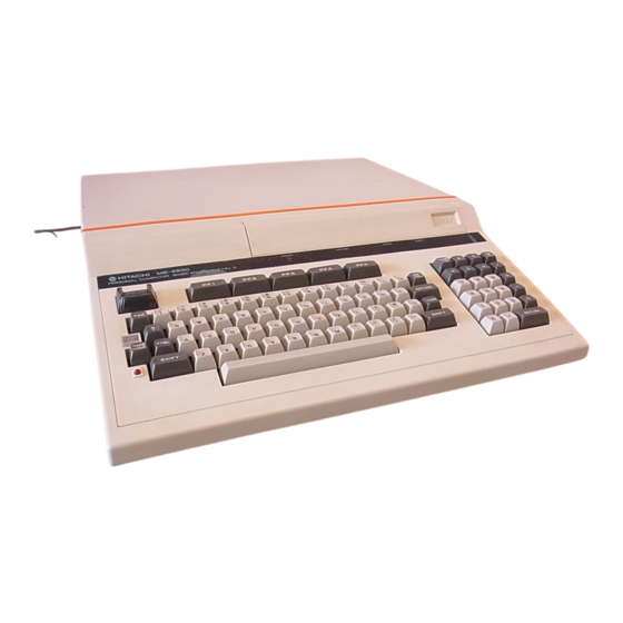
Related Manuals for Hitachi MB-6890


Summary of Contents for Hitachi MB-6890
- Page 1 HITACHI PERSONAL COMPUTER MB’6890 SERVICE MANUAL 0.3012...
- Page 2 COMPUTER HITACHI PERSONAL MB-6890 SERVICE MANUAL 30.1.2.1...
- Page 3 Index » General Features Specification ..each block name used I.C’s » Function » ..circuit Explanation Memory ..¢iii@;i== Adjustment ..Service points ....switches inbuilt usage Trouble shootings ....102 method check Operation circuit Basic diagram P.C.B. layout Basic block each Waveform...
-
Page 4: General
General level having BASIC high multi personal computer, MB-6890 purpose programming. language achieved from h i g h d ‹ m ‹ H d requirement users future expansion system. built interfaces Features command char with colour graphic display separate Seven colour. - Page 5 signal. Connector 3-2_ Recorder(CASSETTEL Cassette Tape direction direction Signal Signal (CPU (CPU out) remote +--~ * - ’ * record remote * - - * |Play * - ‘ Light Penn./PEN) direction direction Signal Signal Out) (CPU (CPU Out) 7675? f137§vV ‘...
- Page 6 PRINTER INTERFACE(PRINTER) directien Qpin direction Signal filo. S3151 (CPU out) (CPU out) STRB --» ~_-~ ’_ ---» -_» --» ’ A i ; T < BUSY --» »-_- Memory expansion (RAM3, RAM4 p i 1 1 Q direction directicn RAM4 RAM3 RAM3 RA114...
- Page 7 Ihterface expansion (I/F-I I/F-6) ipinppin direction direction Signal Signal (CPU -out) (cPU- out) -4-_~ ---» -~-» --» ---» ’ »--» --» ‘ ---- ---A --» ---» --» 4--» ---- --» --» --» ’ ‘ ‘ " E555 EXROM-KIL ‘ E356 11/w --»...
- Page 8 Explanation each part Operation panel ~»,‘ ,.., ‘ _ - ~"’"T »-= " ’ V" f_ _’ operation panel ~ W " C 5 G 5 ? <@@fafi'H switches "fHfi@ inside cover) .,’i’;i;@;_:_ ’i keyboard S W 5 - C C h i RESET Switch votufvia...
- Page 9 @ Interface. sion -1~»,$-513 (I/F Qlight (DPW) Light (BAP-3700) """i monitor fiCblour (coLoR> monitor colour (c14-2170> @MonochromeMonitor’ (ww) monitor Green (KIZZDSSP) ins-zazc. Rs~z32c Other which equipment RS-232C interface. isprinter (PMNTER) interface expansion pairs connectors ’ inside MB-6890. pairs connectors expansion memory...
- Page 10 IC’s use. circuit function Type Pf C@SSif19 Unit central HDeso9P/MCeao9L Hmssossp rcse CRTC L.Sl HD4ea21P LCSS HD4sssoP ICS4 ACIA Icse, 1Cs1 Icss 1Cs9 xcsz [css 1Cso,1Cs1 IC54’ IC65’ IC66 IC57 HM4716AP-1 ICss,1Cs9 Icvo IC71 IC12, IC73, IC75 IC14, 1C1s, Qrcs /mnzsasc-ssc BASIC uPD2364C-331...
- Page 11 circuit type function IC111 Icas, IC51, HD74LSl57P de-selector/rfzultiplexer ICI" Icus HD74LSI58P req! HD14LS1e4P IC42 __§g_ parallel ahlft shift sN14Ls1seP reg. "" 1ca91c11, IC81, xcsz HD74LSl74P rcse, ICIOS, XC109 flip type flop Icus _:ET " -’ HD74LSl75P Icue gate sN741.s245N arcs tranceiver Seleeterhultiplexe- data...
-
Page 12: Function Of
HD6809P/MC6809L Unit Micro Processing MTU: arrangement GND------~-----V" E51 HA|_r’-._--._ ..-. H," Non-Mukabln lnwrum ----- ------ xYAL_ _____ _____ G y m | \ ¢ " U 9 K RMIUMI ~"’ - ’-"~~ SXTAL _____En _______ Icwnd Immun: Request FIRQ -~--~~~--~- ¢-| ____ _____R___t... - Page 13 entire system.This used reset simple network that peripherals higher threshold voltage ensures before reset state Processor. *HALT running level this input will stop cause remainhelted instruction indefinitely present When driven indicat- without loss data. halted, High output also which indicates buses high impedance.
- Page 14 Maskable (NMI) Interrupt nonmaskable negative this input that interrupt edge requests Anon-maskeble inhibited generated. interrupt cannot sequence also priority than software higher E I R Q , I R Q program, interrupt. Request(FIRQ) Fast-Interrupt level this input will initiate fast interrupt sequence provided...
- Page 15 line enables data transfers Data Bus. state input buffers data transferred from line signal device been selected. High sets buffers transfer data bus. output present enable pulse address enabled when proper Reset(RES) bits active line used reset register logical This line used Low.
- Page 16 Peripheral "Read read Register Low. Data Output lines corresponding programmed outputs. Data A" operation when data peripheral This will voltage data read properly than volts logic less lines than output greater lines Loading such that volt logic output output. reach full data these...
- Page 17 Enable(E) Enable signal,E, high impedance compatible input that enables input/output data buffers clocks data from ACIA. Read/Write(R/W) line impedance high input that compatible used control direction data flow through ACIA’s input/output data interface, When High(MPU Read cycle), ACIA drivers turned output selected register...
- Page 18 CC>ntrol Modem limited control permit functions that includes ACIA severa andDCD. included CTS,RTS functions modem. peripheral Send(CTS) Clear automatic control provides compatible input This high impedance modem link communications transmitting Transmit Register Empty(TDRE) Data active inhibiting output bit. atatus Send(RTS) Request modem control...
- Page 19 NSYNC) Vertical Sync (RS) Select Register which verti- level signal provides VSYNC active H i g h the address’ used select signal (RS) Select Register device. display When RS is synchronization of the CRTC. and 18 control registers register RS is and when selected the address...
- Page 20 Chip Select active (EE) content outputted memory data line Basic Monitor written three System pieces Program (uPD2364C-331, pPD2363C-332) MB-6890. Address allocated Address shown table 5-2. decoder TABLE R OM Address /1PD2se4c-aao A oo o BFFF ,,PDz3e4c-331 c ooo n1=z=1= »~ --Q-QQ "UU...
- Page 21 ’igl?Q2332C»§328,§, Rom) (4,096 MASK BYTE CSZEEE v¢¢Ae EER E ! I B E EIEEU DZGNU D’ Address M _ A -~~- .Data m_g, ..f5T.CSz Chip Select ---~ Fig. uPD232C-328 Mask (Read only Memory) used character Byte M -6890. generator address (4KB) Memory...
- Page 22 HDZQEQS (Quadfllpfe 2‘i|’1DUt Positive NAND Gates) WØsw " " ’ ’ l’_ nnuunn ’lilvugeavgns 5-10 Fig. input NAND Gate. pieces consist 5-10 connect drawing. pins omitted wiring VCC, earth line. line input Gate. pieces consist 5-11 (Quadrupie 2-input positive Gates) vcc(5V .,‘, ,¢)_ QTQT...
- Page 23 Open CoHector Output) 5’ lF.’§l " ’F > Fig. 5-13 inverters. Each collector consist from pieces Inverter 5-13 open MB-6890 circuit-drawing.different each required resistor output collector. used mark Inverter open "\ ‘\\ Output Regulator Inverter /»" v"\ collector collector...
- Page 24 HD74l;S08F¥‘ (Quedrupfe 2-input Positive Gates) (svn ’»3| §¢; 5-15 Fig. consist 5-15 pieces gate. (Triple 3-input NAND Gates) W’ S-16 Fig. 5-16 consists pieces NAND gate. truth table shown S-17. fig. Input Output utput V A p B l C .LIL L|H|L HLIL...
- Page 25 H’5?14¢$;l¥F§,. (Triple -input Positive Gates) V;/A ’ » gal II? ’I Is[’Ir Fig. 5-18 5-18 consist pieces input Gate. below Fiq- 5-19- truth table shown Input Output ____ lnput Output (Hex Schnutt-TjiggerInverters) ISI) ’l 5-20 Fig. 5-20 consists pieces inverters. from diffgpengg regular...
- Page 26 REQUl@f Inverter inverters circuit diagram, MB689O shown opposite. Trigger Inverter Inverter Regular Trigger Schmitt Inverter -r--- (HD74LS|4P) 5-2| Input HDZ4ES3d§ Gate) NAND Positive (8-input ’il 5-22 input NAND gate figure when Ouput goes (A-G) Output Input when input goes (SV) CUf"SiS’CS 4pcs input...
- Page 27 Table "L" possible "H" X... rising edge, +... Previous state Previous state Qo...Q Q ..Q EB IEIEIEI EI III I I I condition maintainsprevious changes, output input Even IIIIII IEIIEI rise. does clock edge l1llIl IIIIEI-B Q~» when changes does change even period.
- Page 28 ’ HD14IES93F!? digit Input A-Output counter. (4-mt Bkmry Counter) digit Input B-Output counter ’NTT made counter connecting output input EIIIIIIIIIIIIIIH INPUT vcr: 5-28 Truth Table Table digit counter Cgunt *Truth Table between relationship reset input ’ digit made case counter connecting input written...
- Page 29 ZSAEP I-lDZ4E.S\ 5-29 Buffer Gates Consists pieces three (Quadruple state gates with. Outputs() When control input Low, between Three-State space input output becomes buffer output " 3’ " V" becomes High Impedance "HZ" when control input ’H EH’ (H). > |¢...
- Page 30 5’7 table Input Output Select Enable table relationship X--~"H" both "L "H" Acceptable t a . b l ‹ I 1 1 D l . 1 t Output Select Enablg Y,IY. IHJH HITTHIITIH lG,=Gu Acceptable both "H" : H " "L HDNESISIP 5-32...
- Page 31 (Dual 4-Line I-Line Data Selectors/Multiplexers) Input Slrcbc (SV) Select Cgyjgput ’Id ll!! ;"| UI’ 5-33 consists pair Multi- plexers. » Sdeci Multiplexer device which similar Sfmbt Input Output function switch rotary which_take_s D-L-.. a n - I .--»-.U » outpuii ll-UNI |\|¢|ly .|.l||J\-I...
- Page 32 HD74lLSl51FF (Quadruple 2-Line l-Line Data Selectors/MultiplexerS(Nonlnverted Outputs)) 5-34 data selector/multiplexer which select data from Input having Input Output two, pairs (SV) ,__ pl.1 package. Strobe select $ h & | common outputs. When strobe input "H" _-lm becomes"LI output strobe input "L", input...
- Page 33 (4-Line I6-Line Decoder/Demulb with iplexer Open Collector Output) EEEE BIEIIIBH EI 5-36 ABCD IS Z line-16 line d9CgdEr_ Qutput Q O Q 1 5 collector. open " IIBBIIEIB EIHIEUB 5-35 (HD14IS9P) ’rrunh s-I2 Table IUPUt Output QJQtQJQnQ.QJ Q.Q,Q,IQ1i Q¢ G,G,D Q, Q.Q1Q.
- Page 34 SNZ4Sl 63l\£ (Synchronous 4-bit Binary Counter (Synchronous C|ear)) Output (SV) with E n o m 5-37 digit counter pxeset 6¥ Synchronous Load function. U5 U5 Il _This counter §gg; ,G» with done Preset preset programmable, "L" When applying with clock. synchronization shoul which...
- Page 35 I-IDZ4ESI64F!¥ output parallel (8-bar Parallel-our Shift consists 5-39 Regster) register. shift internal gates input serial El2f§§§i_____ input either Therefore, included. ’ data data, processincx during "L" prohibited. input Synchronous input Clear shifted data pulse. clock dege rising 5-LO chart time ~;V_B.,m 5-13.
- Page 36 shift load register parallel Synchronized 5-41 SNUESIGBEE3 select states. Serial Input Parallel/Serial (8-bit (SI) output serial input shift from Serial Register) Shift’ Output parrallel order from Shift data serial (A-H) inputs (A-H). Having input (S/L) serial belongs parrallel input output (SI), 15v1smn Cleo?
- Page 37 S-I4 HD74LS174P, Q output does exist. ‘c|¢¢k Clear X...Acceptable both +...Rising edge. §. Qo...Previous status H D I 4 E S H 5 F ! - Ed3e’T"ig3 ’ed 5-Ala D-tl/535 consists (Quadruple lines Flip Flop. Difference betweer Clear) with HD74LS1Z§P this chip Flops...
- Page 38 HD74§525ZE§ Data (Quadruple I-Line Selectors/Multiplexers 2-Line with three State outputs Selectors/Multiplexers Data consist Inputs from data (A,B) which decide status Three-State (with Noninverted each output select, output control which Outputs)) common outputs. When control output outputs High Impedance, when v¢¢?:‘Sf» rf‘f=I4A output status data...
- Page 39 HDZ4ES36Z’AE§ (Hex Drivers with Three- State Outputs) tri-state consists driver with outpi 5-48 piece combined pieces pieces gates each__and E’ then connected input when control (G1, G2). ’Q control input (G1, low, output space when becomes buffer between input "HZ". High Impedance output...
- Page 40 5-51 consists Schmitt trigger inverters, (Quadrupre Line Receivers) receiver control each with line input.. control Contrql (5V) reslstance control connectlnq lnput lnput pln, m [Fl thresh-hold voltage changed. cPntrol2AcontrQ! 5 V ) ,» Jntrol 4‘ "" input "" input_ S lin ’GND Circuit &S2...
- Page 41 STRUCTURE circuit MB-6890’s block diagram. structure figure Shown E16-l " ’T below. "_;’ explained 1" » EXTAL Clock 6809 nerator J -_.. f":""’;"_| ’ Trace _G?§¢ ’u Timing signal Counte- block |"""’_ Generate CRTC L___ ~‘ ’ ,_-.___-_---.---1. ’ Agdr gggnecti Øweeai...
- Page 42 [one of page 40-44 missing]...
- Page 43 Supplied monochrome display. Keyboard MB-6890 hardware method. This scan method done counting hori- zontal synchronize signal their equal frequency signal, then scanning decoder IC86...
- Page 44 Cassette Load SAVE Circuit circuit Cassette SAVE convert data signal from serial signals (Asynchronous Communications ACIA Interface Adaptor). This signal Shift converted (Frequency Keying) signals which signals dividing then generated signal, outputted SAVE signal Recorder. Cassette Circuit Cassette Load convert played signals from...
- Page 45 (I)D|PSW Internal Register &l Structure ’Addres Register Data Circflit FuI1CtilO1T1 Name READ wam-: sFFcx anmx >< BK=-x’,.i |lC98 1 1 s ? i ‹ § t § v r { f \ 1 I \ f\1I\CtiO1l\fg;; sr-*Pcs >< ?5E§ g&§?} SFFCA Timer1RQ lxcm...
- Page 46 6 2. sN74Ls245N RAM3,RAM4’ Connector HDGBOQP/MCSSOQL - gufgf " " " " " ’ " " |f4~vPs: 74Ls367AP Connector AavAa»|F4~oF5; R0MJMM.W&AmLcRmet¢ ABQ-’A8\3>RAM +5V1cz4 z c2z+5V ddress BOMB -e> »- 2’ 1/F1~4/F6 ddres KSNMU ~A|5 Mousse. ENiMousse. ’/F~1’~’/F~6 QECDEfE‘1"f"T HALT * " ~ --»...
- Page 47 Table function c-neo-sen. Register QØigiki?-Y Mode Meds I _i g Characteq t Uanormali &¥§§;? Black rite & Blue s’ Graphic everse Magenta 1 i0 Green Cyan Yellow White function Table &4 Register ’ Function Mode Mode K B N M 1 P r ? h ’ b i Mode KBIRQProhi YSHIFTIA...
- Page 48 decoder circuit address decode This circuit allocated address expansion connectors circuit shown 6-5. circuit diagram Figure shown Figure decoded standard incorporated address address upper (AB15-ABM) IC33. outputted Thesetare signal, level address $4000-$7FFF signal, level address $000-$3FFF. which address signal outputted extension main unit...
- Page 49 ICIBB ]C2| g : § § ‹ § § , I c 1 ,>0, 141.s1a9P |1025 PJ-U .> > fcziv IC29 A813 ’cm ICZ9 » .IICZS ’IC26 » When 1c33 5FFoo~$r-’Far ’H’ Level Decoder Circuit Main Fig. Address Parts IC12 |¢3Q 74LS138P 14|_S3op...
- Page 50 XC 33 " PAMI \ § J - s s r r r C 3 ’ Level ’I xc 33 ii-931 lfegel 3 ’ lC137 74LS139P A89~$EL _ / § A _ § ? ‹ f Connector Expansion WEEE T815 ’...
- Page 51 Timing signal generator. 6-4-1 clock specification System according various clock generating clock circuit, generator written ification. Each clock specification clock system spec describes Fig. 6-6. circuit below general circuit 6-4-2 Clock generator circuit circuit. clock clock Fig. shows generator generator oscillator 32.256 Oscillator...
- Page 52 P S V Aooorcx BMC* oorcx 7 > 4 O C - I P C K JI’ IC_38 spares; GRENB 53003522 IGMCK IC43 22 18 |C34 4Mc»< " f» 74\_so2P |C42 socns~aL xc 35 ’ 74Ls1s1P as a: c»< lcas CAS01 »o "...
-
Page 53: Explanation
Circuits Generating 6-4-3 Signals System written Fig. generating circuit chart signal Timing system MHZ) which (l.008 Fig. 6-9. signal signals timing charts each l6.l28 then outputted shifted clock MCK, IC42 generator inputted signals combining these signals, system output through QB...QH. their generating each... - Page 54 modeChBHQ9 circuit character 6-4-4 Display circuit IC38) circuit character switching (fig. 6-8, display mode side, characters. input display characters change mode Each characters inputted. DOTCK, LOAD, CHRCK GRENBLE signal when IC38 input (SELECT terminal) characters mode, character when High Level, outputted IC38 level,...
- Page 55 !C50 IC47 ’ vide Sigma genera 14|.s74AP 74LSOOP ale: o-mf ’ Ssmnmnnznm "’5V ’ IC47 2’ $ IC49 » ’ ». |¢5Q xn xx M/us Eire IC49 [Cys lC396Q, » . ¢ » . 74|_503p ’ ’ " " " Ø ; , § ‹ . § -»= |:=- ~ ’S...
- Page 56 dlll lCl07@ lCl3C| lCI36 IlNTERL A-CE- se’ "+5v ’ |c13o __..¢_ 74L$74AP FIAo lCl07’_fi (AO) RAAI lllllll RAA2 ’2 " RAA5 ICl4| ’S |c14a ’I4LSO8P 74LS157P circuit Interlace switching 5-I4 Interlace/Non !--s;=5#$= 5 (lClI6fiPlX’L| V L I 1 ’ RAA1 flcxas QPU) f"5 5~=(lcharacter...
- Page 57 ’ R & 3 ¥L $w2P - $4& "" $429 gaze anal $757 $7E6 9" |7¢| Fig. "CRT address Normal Mode 8Uch ‘ " " " - _ " - - _ _ - _ _ _ $427 ----- SC27 [yew slozr :goo...
- Page 58 ‘ 6-4-7 conversion switch circuit Display address Basic resolution mode display mode. Master normal mode high resolution divided direction high character raster mode, with This circuit make character byte address. display conversion 6-l6 shows main address switch circuit. Fig. part ="H"level circuit.
- Page 59 combination colour Displayed Colour Pig. .642 kolou ’go Flack blue ed’ aqen rØen ello white! meanin Colour Fig. biifo bitl bitz r?6§ IUQN ‹ d 3 N revere Graphi ’H’ xcssc] 1d@FF edOFF Norma Chara. ICS4 16355 :ces ’t xcsv RAM¢ir¢...
- Page 60 SØ%Ø3Y ’FA "Ø (reffeSheperiodI|per§c§ § » \g.L0|S5’$-,E ’ Ø f § § ‘ ‹ 2 § § § § ’ Signa ’ ’ sa§§2§§g X§a§§Ø;§;w1X@§a§§;@YAD§aadfess aadfess colum ’ ’ swigcg signql ’ mn’ ’ adggesx dggØsx ggdggØs Adare MQLQW a-»reSS address ’...
- Page 61 accessed) (other display address used mode this page case, character mode column address. changing address same clock cycle enough, display address display, piece continuous equaling column address ifit regarded each address column address signal output same. described table 6-lO. circuit 6-5-2 Colour Basic...
- Page 62 Video Block Signal Generator each explanation 6-21. Block shown Video Signal Generator circuit below. Circuit 6-6-1 Character Generator circuit, circuit. character generator 6-22 shows character generator according data required character change output each character. dots structure interlace mode interlace mode terminal) (chip select...
- Page 63 nAA| SA’ » ’xc|o7 sw.; 2 . E § yP0233Z3328 Circuit Fig. &42 Character Generator ucuz Q 5 f ’ § . ‹ t C Co1ourRAM |cuaetc Ionochrome Data video ideo Slgnalt si onochr 033051 generat»r s1qnal §engra§~r ’CU? lrcul gaia glt n-s- ‘Øge?at...
- Page 64 Byte’-V \‘ $sbyi_e & ’ arg? - - ~ Whyte ilefn @Interlac EØgeh ern) Common fi Qich ern) Reoordin" Concept 6-23 Character ~enerato1= _’_ »¢ C a m |c1 12 :CUZ 74|__3153p SØi 5 .4 axcszs Qazasaaalpzasnu 535% 4 zasa»:g|4zA5A4A Øs ’I4 ‘|...
- Page 65 signals. this conversion period, shift/Load signals inputted ICll7 which makes possible video output signal during display period. Data from colour makes timing each character 1c115 input (LOAD signal)to with synchronize brightness which signal derived from ICll7. brightness combined signal with display signal (REV...
- Page 66 Background colour |C’|’|5 Infomation 74LS174P BB" LOAD ’O CISS’ |‘LCI5i ICIIB ns , ICVI6 ’ 74LS175P 74L$158P ’ | 5 V 1’5V 31Cl3i 1C|I5 f-¢ v¢c IC|32 ’ ’ BIIIB 2sc121afi/' 2 r ¢ » | e § § ’* Tn/\G\ sro c x Termlnal...
- Page 67 circuit Keyboard keyboard. structure general 6-28 shows Figure l5.75KHZ) X-counter Horizontal pulse clock (scan signal Input inputted down count startsthe count output (IClOl. IClO2) UECUUQP decoder "L" scans. this, output (IC86). IC102) counter singal (output input carry (IClO2) starts down counter count same...
- Page 68 ’ ’t Load 4’ Cassette Cqlicul- load circuit clrcult Load cassette cassette 6-32 Fig. Flg. input/output timing. r."___ "_‘ ""‘ """f‘| Power *" §§¥fix lcvo ’ LS151P F § * - 4 - a f - | ~ ---- ’-- matched signal ’...
- Page 69 l C l 2 2 lC|23 ICI24 74LS93P 74LS93P 74LS93P r+zv +55v £m_(1_onsMH ) : ic w?; . v¢¢ lgfa gig. xmzamcx ’ zcuzz 2’ xc|23 §$1¢... » _ - - " 2 "gn |f’1 H’ SICS2 " 74|_s1s’/P " ¢:zz’§7,, rc9| rczzsl...
- Page 70 |+1.66us-I g1C9| 2.4.KHI~ lcxzs @9111 lcuzs from S l g SAVE ICIZS ICB4 Qfinput output Zpgie " ____ lctze |ClZ6 lC|25 tfl-,us ’3 " lC|25 "2c 2 KH1. UUUU1 ¥1§3’1putHH ‘ ICIQOZP ,._.m4,,S jilinput "’| 74|_s14AP 6-30 Fig. :CRS circuit SAVE Cassette r-*"*’*"’I...
- Page 71 Cassette Load circuit demodulate signal (sine l.2KHZ wave 2.4KHZ) digital signals. signals from recorder tape limited 1.2Vpp limitter (D3.D4) input ICl27 then inputted ICl28 (Voltage Controlled Oscillator). ICl28 standard voltage this circuit. ICl28 voltage which comparater output digital converted data signal ICl28 relationship...
- Page 72 communication RS232C ICl2O (HD75l89P) (HD75ll88P) ICll9 features. have following interface receive/sending line driver) HD75l88P (Quad limit date switching level input which outputsthe upper voltage High this circuit, VCC=+l2V, VEE). (VCC, lower limit Power voltage VEE=-12V line driver) HD75189P (Quad (Max. input f3OV) inverterst...
- Page 73 L/$31 T i I I \ ‹ | 1 § 2 [ 3 | | ’ 5 1 5 $ l 8 | 9 | l D I l l | ‘ 1 2 | jsrØpxfisrifpzi lsqnr’ |s>amy B111 B115 asia 5.15 Serial...
- Page 74 from’ =»-mnVi‘ |curfi Rswsw Cassette nszzzc ’ra ’ C f=\m f1 " lC12S»@ mcusiij lCHS@ lcllgig "g: XCB4 nszszc ’ from » OI1lY :clams m\_s| ’O H 13 ’T |fC§l .I U Icgz ’f Ern. ’J IC54 sz/w ’fm Hmeasop circuit Peripheral control...
- Page 75 |C105 74LS05P 2; 21 :I 3 5,4-5 ¢,,,-¢ [css "’ Tl 5. an-9 2’ p g - 3 »r rcsu »=s¢ ’ #R £528 sig. TCIOS 1-:EA 35-| P8313 C|O5 E‘2 ’Z rcnos 95" 1c|o5 QE" QE-5 ICIO5 1352 E‘ Ices ai);...
- Page 76 Other circuit circuit 6-9-1 generating Sound described circuit fig. 6-44. generating Sound SEL,eoLmd decoder address MUSIC rising output edge system 6-45 shows data IC93. Fig. after latching timing signal outputted circuit. chart generating Sound circuit IC93 amplified sound signals which made amp.
-
Page 77: Memory Map
block interface 6-9-2 expansion system which enable incorporated expansion connectors level master memory used expansion connectors also dynamic expand memory user Following expansion power. additional peripherals easy interface block. expansion explanation system connectors general expansion connected data address inside main unit control decode... - Page 78 k)RAM (;)standard (b)RAM8KByte expansion expansion maxi ’ " ’ ’ ~------ ---~-- --__ 1512 (xaxbyte *RAM__ ____ __..__ ______ $4000 area _RAM » 1_;_E_- $8000 erna =1rd anslon ,:§f£>§§_______ tØ Raid* SA000 ’__ ‘ usbyte) (3KbytØ ’ ______ _____ ’ SC000 ’...
- Page 79 terminal expansion nmamemory SN74LS245N ldata RAM’ ’ » data ’ B y t e - address £a9sEL Qlrcu asia? g’ ’ AESEL RAMexpans’ termlnal expanslon memory 5320 ($C000-SEFFP) 59FFF addre select Ølg (xsxbytg ’ (=A9 ) serrs select ‘ pAMexpansi (Waco) F§...
- Page 80 Unit Block 6-10 Power which consistS supply insulated regulator Switching unit power power obtained. circuit. Also, output generating single forward ON-OFF small obtained. Further, +l2V voltage amp. down output, output chopping circuit, terminal dropper totally regulator using -SV/-12V gained -l2V). -5V, (i.e.
- Page 81 circuit. details regulated 6-49 explains Fig. D100 flows through flows D100 when through becomes stored T100. Total wheel diode. When energy regulated output. which makes ICl00 width control R112 C112 connect pulse nanillnfinn r " i ’ r r ’ n i + ’ i n h11’i‘|1’...
- Page 82 6-10-5 Other circuit circuit. unit block have following protection Power circuit Rush control current circuit, rush current control resistor regulating when current power efficiency when thyristor both conducts, controlled power direction done forward regulation only that improved static condition. serial fuse which inserted...
- Page 83 Level-3 Basic Master configulation standard memory expanded memory each memory refer Please Fig. described address decimal 0000 work areaw ’15 0400 __" ______ _______ ----- Hlsplaywnnr < CA1nn, oro-r ffm, area. --am ____ work area USE! 1> a d d r e s s _ _ " ‘ "...
-
Page 84: Adjustment
ADJUSTMENT METHOD circuit adjustment 8-1. main power oscillator 2V+/- sine oscillator, output Prepare wave connecting jack Fig. cassette shown nugger oscillation. 1.7K number terminal inserting ohm,seria1 measuring then input impedance, voltmetre which than more TP13 TPl4 shown between voltage test measure 8-1. - Page 85 Timinq Adjustment System required. replace 1(HD6809P/MC6809L), following procedure unit. MPU(ICl) number Confirm grade necessity number done confirmation grade wires Cl87. jumper combination their avilability Table shows each shows position wires Cl87. Fig. jumper wires Cl87. jumper Confirm grade 8-4. shown Fig.
- Page 86 CAPACITY switch operation panelthen switch "l" MODE power Press \l4l72\ FRE(H)[ confirm display command PRINT screen Input ’ BASIC version HITACHI LEVEL high This case Microsoft iiigglgggeØcØriieg resolution mode. Ready PREM) input PRINT confirmation display 14172 Ready "2W. switch return...
- Page 87 POINTS SERVICE this with section actual unit. photo’s change cards option sold photo separately. Remove screws case upper which hold case upper then Fig.9-2 Fig.9-l, obtained. §§%§§$s&3£i ,;§§§$5§, F l g Fig.9-2 extension card screwsfi Loose upper cover eqaaaszrf _;~,_ F1g,9-2.
- Page 88 screwsgg P.C.B. By loosening BM-A removed Fig.9-5, BM-A P.C.B f__Db Fig.9-6. Via’-:H ’Q ~*’ ..._ g§;jy;_ ’ ’ ’mf fall# /I .-..;_z ‘=.Ø»v~. =_,..,, *Øs ‹ _ | ;j‘ ...=::" " ‹ ’K "T:%j"_’;1;¥;;t , , , % ’ , _ ’ii’...
- Page 89 Switch usage; ELILT different switches built Level-3,four conditions. various initial_state when switch switch(SW); setting power switch Chip switch(CS1); setting MODE content Chip switch(CS3): setting RS232C baud rate thecommunicatiom Chip switch(CS4); setting condition RS232C. When setting changes required, should done after turning power.
- Page 90 switch(SW) different switches shown Fig.1O-2. switch consist initial after each switch, states position power TablelO-l. switch shows state("1") positioned each white OPen they to{}side i n , p o s i t i o n . Close state("O") meaning TablelO-1. indicate switches’...
- Page 91 switch (CSl) Chip ofth9 setting content (CSl) change Chip switch described condition which setting standard switch. MODE corresponding connected switch previously, MODE selection ch/line ch/line this, switch No.3. connected switch MODE switch. MODE possible 0 P @ 1 ‘ 3 t i 0 V ~ f ‘...
- Page 92 Chip switch(CS4) condition defines sending/receiving chip switcn(CS4) communication RS232C interface. outputted inserted outputted [___ ~ ’ \ ’ / 1 - ’ * ‘ ~ 56 psi outputted sig. outputted :O ml ’ EO OE active sig. becomes f"DCD becomes earthed 5__l_.§__,_.
- Page 93 Pzewri ’NE SCREEN *5V. " +|2V. ’norm (power unit) pin? (video signal generator) ag at § § pin? (timing signal generator) EØion sig; 433 ) (RAM) ’ e2§%;§l§ (data bus) gulse address decoder oircu QØsgai 1‘ § IGJQ. IG-.I1’1§Et, slggmil fl;...
- Page 94 NORMAL @ ‘ r > A r A ’n "g" Eevel. " - § 3 * L 2 ~ 9 3 1 Gi" lc" lC27 |C12 lc" ncnaa |¢91 |4335 IC" ’ ’%¢5 ‘t Eine? 2252 35,1 egine? |c29 ’ ucsz ncaa ’...
- Page 95 SIGNAL NDRMA TIMING qn5§§ IYES ’ ""’ ’YW it38? ulse i i3 D i n ’C4 %g§§ie§ pg ‘ ‹ a § l ‘ {f i pins IC38 5?33. IC36 IC40 No w correct » ’_ tput corr-~ |C46 IC37 pln.
- Page 96 DATA- PRQM _RAM NOT- Running below program each form wave which described chapter s>§§?f1ei;3,; o¥a¥§" POKE &H6000. " corox I=I+1ZIF 1>1s lC56~lC75- COLOR I Z P R I N T H I T A C H I lnØ -2¢§§§1&§§_ " GOTO Puls ’cw...
- Page 97 IDEO SIGNALS riqhØnea grciififfØpl _ grciifi ffØpl »ulSe *p ar C117 15pin? pin5,7,1O; pulse H " ? inputted ‘ l29,9 |ci|5 ’ ¢ :cms P1-1lS@ uczs ~utputted -pin? ICIIG vcwl ncns -ulse nputted 18,15~‘ ‘ "~utted 1&g » 9pin? ; ; S ’ ; C 1 3 =’n? colour ucuoo...
- Page 98 INCORRECT ENTRY should observed waveform when pressed orking? Ic99, pear » r’.zz:.’|’ ¢ stilke @5121-1-a -i».n.-.4- ’ ’ &3 puls- inputted~to >’9p1 chlp connec ,¢w2 contact keyboard » ulse appear Ol&1O ‘ lCl0I lCl02 outpu’ appear ulse IC9O pear ulse »...
- Page 99 DEFECT GRAPHIC MODE H. 7 »~ ISS. work :Cuz |Cl29 IC39 4,lO&l3pin? |C40 ICSI ICH! ICII4 Defective...
- Page 100 QPEECATE DOES *waveform should observec after release time mask -nputted PGKE sfHFz=n4,c eve* sec. ’ ICli :cas ’cm ~uls- ’nputted sec. IC1~,~¢’ -ulse lnputted sec.»t» IC22,2~‘ :cas waveform should observed after outputting sound program 11qp pe;;_’;; ex), BEEPZGOTO1 ulse lnputted 93,3pid _ulS_ "...
- Page 101 B=§10} SAVE/LOAD CASSETTE Only SAVE :ca_n’t LOAD ’ done ‘ ognes pin-? " *iapee output in_ kh.-g p *record ’ *relay pin;norma YØs circuit ’ ’tt raigiigaxe ‘B) ‘ """’ correctly ICll djus 9pin;norma» R109 misadjus ,CH7 C1If.l, 4&9 cg>»ut ’...
- Page 102 fliililjgf PRINT OUTPUT -ppear f-in printer ulse outputted IC85 ICWS LIGHT PEN-DOES WORK orrectly -djusted R " mlssadj stment ppear ’ &2 -pln defect utputted ’ ’ » ‘ outputted 9p1n ‘ Defective...
- Page 103 ABNORMAL»POWER ’ IIIKUB nector pull then from power adjustment) unit (;efer; load dumuv power f ‘ f \ 1 \ l \ eonuoe- power (from lead ‘tage -~TH13¢ output volta-- load defec appe-#L 45,+12v » only ‘ abno power justment ’...
-
Page 104: Trouble
METHOD OPERATION CHECK trouble repair, After shooting fgllgwing qparatign ghggk quired. 12-1. Connecting method; normal operation check inbuilt switches "CLOSE" No.1/»No.3 "OPEN" ,No.4~»No.8 condition(dip switch setting switch "0"). front panel MODE Fig.l2-l check shown operation connect perpherals Next, »-...»‘»-.nl-~ annflinnl _,av-kann L_--- 1.1_-... - Page 105 file item content test program czlxs-c MOTOR, interface SAVE ,vEP_rFY, cassette ON-OFF data KY-PR interface test printer ‘ line control & SPK-C varible test speaker sound oscillating sound interface operation LP~C light test line RS2-C interface receive/sending RS-232C operation test...
- Page 106 agus JignØg ’ 1011 wØr ¢ conf; -ceo ’I ¢ Display Mask R O M t ; e s t ’ rogramma~ ¢ correc *="=|’> ’=¢’ HGSK TEST =|=|==|-mv- circui = * = * = * CHECK -ummm ‘ cwrx ff’...
- Page 107 from previous page display display colour igggen o?fi " ¢ E ¥ Ø check colour pre gl k ys Y ES magenta Press Cyan |e5nmN|k@V yellow L--_J black blue green ggØggr §A§Øl gglopgy ilgg ’eerilggCircuit nga:smannusixansu Circuit ’e nga: § § § 221132 33’...
- Page 108 previous page from " a§e screen Press EE§E§ Switch ’cwer ’Øggic aigcter § § @ § h § § @ imin 8S%S§%§3§ gsesf e §Pa§§1 §Qe4 Q EQ-~Øw?’@ 2433 ower mode Screen graphic test Mode Check Graphic keys Press Mode Qggghic BGR-Cl) @§?§E§S§;Ø...
- Page 109 previous from page E218 Øls rgigriggieg t e S f lnterface cassette Screen qrap naml% 5i9"aL aØraaegi » P I ‹ S S l P H l P ¢ q keys as-H- Ready ei § % 3f= ’ ‘ interface gggiette Uerlfy ( Programme...
- Page 110 P a - E e previous from tØsi speaker displav screen test volume speaker nf1rm soun cnanga confirm volume, turn ange sound clrc test screen.of lightlpen Einv-.. |r\nlvru\| uuuuoooco 9¢t .’7 oeonoaaaaur ‘ » inf=@rfa¢@ %ig¥t llIll||| llllillll llillllll lillfllf aauwfa;...
- Page 111 R N"¢( test) mask TEST PRDGRRK REHl|4~1um PlB~S8SO HRSK U l ’ * \ * SCREEN OIHIDTIIAD PQSK TEST *’** ’*’FPRINTtPRINT LOCFITE PRlNT’¢c¢\ca f|DRSl&H7000 " REED FURI’0T0h0 C D D C l V R L ( ’ l H ’ * H 1 D l ( C R $ ’2*l\~1¢ POKE B D R S U - C D D ‹...
- Page 112 test) (fcolour COL-C o.x.o=uxornao scnesw c.o¢.¢uA - r : s 1 Locnrs s.::vnrNr~~- " " ’ 5 YE!-VOM/’ 4»u¢»< cwmg - \ = » 4 » u ¢ » < c w m g Y E ! - V O M / ’ "...
- Page 113 KY PR " prlzgger ¢ lnueruace SCREEN 0-1.0!HIDTHAO LOCRTE }fE7§04&P Tf6T 0¢3IPRlNT’ M*v’ RSCZO) IBLS FORK ~lTOX9 PEDD R$(I) NEX-T DGT9 ’ l Q » ’ R Z ’ » ’ 2 5 A 5 S ’ » ’ 7 S S O ’ sara "...
- Page 114 LPC( test) light LIGHT TEST PROGRRH *l’**¢ 1104"-O’ ***** NITQCHX V O K G - W i l M URKS ***¢* SCREENOIHIDTHBO COL.C|R7|0 PRINT’ ||an-cwovnmfn-on LIC,/~/T 7’¢-xfto-no-meanest P E ¢ 1 l ( S | 7 ) - ( 1 3 | S)|2!(20v7)-(261 9)|3|(30|7) (38v A|(44...
- Page 115 test) interface $2-C(RS~232C SCREEN OIHIDTHQO LOCATE 0-IZPRINT g5-232g T557 Inpug mum’ LCCQTE 0 S 2 P R I N T " ’n~a1~f-15m 1496590 L’ "-- P R I N r = P R 1 N T ’ 1’ERr1’e;HRsc|.H22>1’ ssN2H~:CHRs INPU F R I N T ‘...
-
Page 116: Parts List
PARTS LIST position circuit circuit J’ r’ef’ f’ r’ e Part qtf’ HQMQ part PPQY CGW* MB-6881 oo9oo P~1ne\ A Msfeseo ’ oaxoo swow 07100 cover; uovev osxso » C10-118 osooo QUQVQB MP-3030 osooo O 3 \ f % Q U.cu1Q1‘... - Page 117 HD74LS32P ’L Mmssz 02100 :cas HD74LS02P mrsaso 06000 IC34 06000 xcss HD74LS66P MP-1010A 07100 :cas Hmesossn Ms-5090 05030 IC37 sm4s1s3N MB-6890 03500 rcss HU74LSl57P » 02200 icss HD74LSl7-IP MB-ease 05300 1c40 HD74LS283P MB-0090 01300 1c41 HD74LS367AP Ma-esac 04200 HD74LSl64P oosoo...
- Page 118 » MB-0000 00000 1c95 1~1m41.s051> » 00000 1c90 11m41.s0s1=> MP-3530 01100 L S I lC97 I-{D74LS32P MB-6881 02100 xcss HD74LSl2SAP MB-6890 07100 IC99 HD74LS74AP » 05000 IC100 HD74LS04P MB-0000 00000 » LS I 1c101 HM4LS93P MP-3530 03200 ICIOZ » 03200 lCl03 »...
- Page 119 f c \ f ¢ w » 1 L L 3 % c\f¢w»1 PART Name part PQ¢£_‘ref‘ L S I IC124 HUl|LS93P Ma-ssso oazoo 1c12s Hm4LsooP Ma-esso oeooo xcxzs 1~m1u_s14A1> Hm41.s14A1> ossoo » L S I ICIZ7 LM565CN Ma-easo o4soo ICIZS H.D75l0&AP »...
- Page 120 UN I T MB-3159 MB-6590 00100 IC100 ’ 00100 zczoo ’ xcaoo TA79u00sAP 05300 01500 IC400 »Pc14sx2H 2SCZ149L/2SC2931 013.5890 01600 istori trans MB-6890 2SC1096(L) 03300 Qxos 03100 Q130 zs/usa? 2SA733P » 02900 Q200 zsczsxs MB-6890 ’ zsssosx. 00000 Q201 » 2SB605L...
- Page 121 » l33§ acmoa D458 » » MP-asso RDIZEBI ’Zemf zmos Ma-aaso RDIIEBI ZDII9 1351 aDs.ssm zD1so o1ooo » RDISEBI ZD230 MB-6890 lwasl-:az >2_@_y\@y ZD23l » RDIIEBI znaao 1:19 nnxasas zmao » nnzoem ZD43I SJVZY oaaoo \f‘\ +Y\\/ Ma-esso sP2M 1111...
Need help?
Do you have a question about the MB-6890 and is the answer not in the manual?
Questions and answers