Table of Contents
Advertisement
Quick Links
240pin Unbuffered DIMM
based on 2Gb D-die
78FBGA with Lead-Free & Halogen-Free
(RoHS compliant)
datasheet
SAMSUNG ELECTRONICS RESERVES THE RIGHT TO CHANGE PRODUCTS, INFORMATION AND
SPECIFICATIONS WITHOUT NOTICE.
Products and specifications discussed herein are for reference purposes only. All information discussed
herein is provided on an "AS IS" basis, without warranties of any kind.
This document and all information discussed herein remain the sole and exclusive property of Samsung
Electronics. No license of any patent, copyright, mask work, trademark or any other intellectual property
right is granted by one party to the other party under this document, by implication, estoppel or other-
wise.
Samsung products are not intended for use in life support, critical care, medical, safety equipment, or
similar applications where product failure could result in loss of life or personal or physical harm, or any
military or defense application, or any governmental procurement to which special terms or provisions
may apply.
For updates or additional information about Samsung products, contact your nearest Samsung office.
All brand names, trademarks and registered trademarks belong to their respective owners.
ⓒ 2010 Samsung Electronics Co., Ltd. All rights reserved.
- 1 -
Rev. 1.0, Sep. 2010
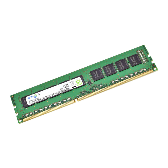
M391B5773DH0
M391B5273DH0
1.35V
Advertisement
Table of Contents

Related Manuals for Samsung M391B5273DH0


Summary of Contents for Samsung M391B5273DH0
- Page 1 Samsung products are not intended for use in life support, critical care, medical, safety equipment, or similar applications where product failure could result in loss of life or personal or physical harm, or any military or defense application, or any governmental procurement to which special terms or provisions may apply.
-
Page 2: Revision History
Rev. 1.0 datasheet DDR3L SDRAM Unbuffered DIMM Revision History Revision No. History Draft Date Remark Editor - First Release Sep. 2010 S.H.Kim - 2 -... -
Page 3: Table Of Contents
17.1 Jitter Notes ... 33 17.2 Timing Parameter Notes... 34 18. Physical Dimensions... 35 18.1 256Mbx8 based 256Mx72 Module (1 Rank) - M391B5773DH0 ... 35 18.2 256Mbx8 based 512Mx72 Module (2 Ranks) - M391B5273DH0 ... 36 datasheet - 3 - Rev. 1.0... -
Page 4: Ddr3L Unbuffered Dimm Ordering Information
Unbuffered DIMM 1. DDR3L Unbuffered DIMM Ordering Information Part Number M391B5773DH0-YF8/H9/K0 M391B5273DH0-YF8/H9/K0 NOTE : 1. "##" - F8/H9/K0 2. F8 - 1066Mbps 7-7-7 / H9 - 1333Mbps 9-9-9 / K0 - 1600Mbps 11-11-11 - DDR3-1600(11-11-11) is backward compatible to DDR3-1333(9-9-9), DDR3-1066(7-7-7) - DDR3-1333(9-9-9) is backward compatible to DDR3-1066(7-7-7) 2. -
Page 5: X72 Dimm Pin Configurations (Front Side/Back Side)
2. CK1,NC and CK1,NC : Used for dual-rank UDIMMs; not used on single-rank UDIMMs, but terminated 3. TEST (pin 167) used by memory bus analysis tools (unused on memory DIMMs) SAMSUNG ELECTRONICS CO., Ltd. reserves the right to change products and specifications without notice. datasheet... -
Page 6: Pin Description
Unbuffered DIMM 5. Pin Description Pin Name Description A0-A14 SDRAM address bus BA0-BA2 SDRAM bank select SDRAM row address strobe SDRAM column address strobe SDRAM write enable S0, S1 DIMM Rank Select Lines CKE0,CKE1 SDRAM clock enable lines ODT0, ODT1 On-die termination control lines DQ0 - DQ63 DIMM memory data bus... -
Page 7: Input/Output Functional Description
Unbuffered DIMM 7. Input/Output Functional Description Symbol Type CK and CK are differential clock inputs. All the DDR3 SDRAM addr/cntl inputs are sampled on the crossing of positive CK0-CK1 SSTL edge of CK and negative edge of CK. Output (read) data is reference to the crossing of CK and CK (Both directions of CK0-CK1 crossing) Activates the SDRAM CK signal when high and deactivates the CK signal when low. -
Page 8: Address Mirroring Feature
The controller must read the SPD and have the capability of de-mirroring the address when accessing the second rank. SAMSUNG DDR3 dual rank UDIMM R/C B(2Rx8) and R/C E(2Rx8) Modules are using Mirrored Addresses mode. datasheet... -
Page 9: Function Block Diagram
Unbuffered DIMM 8. Function Block Diagram: 8.1 2GB, 256Mx72 ECC Module (Populated as 1 rank of x8 DDR3 SDRAMs) DQS0 DQS0 I/O 0 I/O 1 I/O 2 I/O 3 I/O 4 I/O 5 I/O 6 I/O 7 DQS1 DQS1 I/O 0 I/O 1 DQ10 I/O 2... -
Page 10: 4Gb, 512Mx72 Ecc Module (Populated As 2 Ranks Of X8 Ddr3 Sdrams)
Unbuffered DIMM 8.2 4GB, 512Mx72 ECC Module (Populated as 2 ranks of x8 DDR3 SDRAMs) DQS0 DQS0 CS DQS DQS I/O 0 I/O 1 I/O 2 I/O 3 I/O 4 I/O 5 I/O 6 I/O 7 DQS1 DQS1 CS DQS DQS I/O 0 I/O 1 DQ10... -
Page 11: Absolute Maximum Ratings
Unbuffered DIMM 9. Absolute Maximum Ratings 9.1 Absolute Maximum DC Ratings Symbol Parameter Voltage on V pin relative to V Voltage on V pin relative to V Voltage on any pin relative to V Storage Temperature NOTE : 1. Stresses greater than those listed under “Absolute Maximum Ratings” may cause permanent damage to the device. This is a stress rating only and functional operation of the device at these or any other conditions above those indicated in the operational sections of this specification is not implied. -
Page 12: Ac & Dc Input Measurement Levels
Unbuffered DIMM 11. AC & DC Input Measurement Levels 11.1 AC & DC Logic Input Levels for Single-ended Signals [ Table 2 ] Single Ended AC and DC input levels for Command and Address Symbol Parameter (DC90) DC input logic high IH.CA (DC90) DC input logic low... - Page 13 Unbuffered DIMM [ Table 3 ] Single Ended AC and DC input levels for DQ and DM Symbol Parameter (DC90) DC input logic high IH.DQ (DC90) DC input logic low IL.DQ (AC160) AC input logic high IH.DQ (AC160) AC input logic low IL.DQ (AC135) AC input logic high IH.DQ...
-
Page 14: Vref Tolerances
Unbuffered DIMM 11.2 V Tolerances The dc-tolerance limits and ac-noise limits for the reference voltages V (t) as a function of time. (V stands for V (DC) is the linear average of V (t) over a very long period of time (e.g. 1 sec). This average has to meet the min/max requirements of V thermore V (t) may temporarily deviate from V voltage... -
Page 15: Ac And Dc Logic Input Levels For Differential Signals
Unbuffered DIMM 11.3 AC and DC Logic Input Levels for Differential Signals 11.3.1 Differential Signals Definition .DIFF.AC.MIN .DIFF.AC.MAX Figure 3. Definition of differential ac-swing and "time above ac level" tDVAC 11.3.2 Differential Swing Requirement for Clock (CK - CK) and Strobe (DQS - DQS) Symbol Parameter differential input high... - Page 16 Unbuffered DIMM [ Table 4 ] Allowed time before ringback (tDVAC) for CK - CK and DQS - DQS (1.35V) Slew Rate [V/ns] > 4.0 < 1.0 [ Table 5 ] Allowed time before ringback (tDVAC) for CK - CK and DQS - DQS (1.5V) Slew Rate [V/ns] >...
-
Page 17: Single-Ended Requirements For Differential Signals
Unbuffered DIMM 11.3.3 Single-ended Requirements for Differential Signals Each individual component of a differential signal (CK, DQS, CK, DQS) has also to comply with certain requirements for single-ended signals. CK and CK have to approximately reach V half-cycle. DQS, DQS have to reach V min / V max (approximately the ac-levels ( V ing a valid transition. -
Page 18: Differential Input Cross Point Voltage
Unbuffered DIMM 11.3.4 Differential Input Cross Point Voltage To guarantee tight setup and hold times as well as output skew parameters with respect to clock and strobe, each cross point voltage of differential input signals (CK, CK and DQS, DQS) must meet the requirements in below table. The differential input cross point voltage V cross point of true and complement signal to the mid level between of V VSEH [ Table 7 ] Cross point voltage for differential input signals (CK, DQS) : 1.35V... -
Page 19: Slew Rate Definition For Single Ended Input Signals
Unbuffered DIMM 11.4 Slew Rate Definition for Single Ended Input Signals See "Address / Command Setup, Hold and Derating" for single-ended slew rate definitions for address and command signals. See "Data Setup, Hold and Slew Rate Derating" for single-ended slew rate definitions for data signals. 11.5 Slew rate definition for Differential Input Signals Input slew rate for differential signals (CK, CK and DQS, DQS) are defined and measured as shown in below. -
Page 20: Single-Ended Output Slew Rate
Unbuffered DIMM 12.3 Single-ended Output Slew Rate With the reference load for timing measurements, output slew rate for falling and rising edges is defined and measured between V for single ended signals as shown in below. [ Table 12 ] Single ended Output slew rate definition Description Single ended output slew rate for rising edge Single ended output slew rate for falling edge... -
Page 21: Differential Output Slew Rate
Unbuffered DIMM 12.4 Differential Output Slew Rate With the reference load for timing measurements, output slew rate for falling and rising edges is defined and measured between V (AC) for differential signals as shown in below. diff [ Table 14 ] Differential Output slew rate definition Description Differential output slew rate for rising edge Differential output slew rate for falling edge... -
Page 22: Idd Specification Definition
Unbuffered DIMM 13. IDD specification definition Symbol Operating One Bank Active-Precharge Current CKE: High; External clock: On; tCK, nRC, nRAS, CL: Refer to Component Datasheet for detail pattern ; BL: 8 IDD0 Command, Address, Bank Address Inputs: partially toggling ; Data IO: FLOATING; DM:stable at 0; Bank Activity: Cycling with one bank active at a time: 0,0,1,1,2,2,... - Page 23 Rev. 1.0 datasheet DDR3L SDRAM Unbuffered DIMM NOTE : 1) Burst Length: BL8 fixed by MRS: set MR0 A[1,0]=00B 2) Output Buffer Enable: set MR1 A[12] = 0B; set MR1 A[5,1] = 01B; RTT_Nom enable: set MR1 A[9,6,2] = 011B; RTT_Wr enable: set MR2 A[10,9] = 10B 3) Precharge Power Down Mode: set MR0 A12=0B for Slow Exit or MR0 A12=1B for Fast Exit 4) Auto Self-Refresh (ASR): set MR2 A6 = 0B to disable or 1B to enable feature 5) Self-Refresh Temperature Range (SRT): set MR2 A7=0B for normal or 1B for extended temperature range...
-
Page 24: Idd Spec Table
IDD2Q IDD3P IDD3N IDD4R IDD4W IDD5B IDD6 IDD7 IDD8 NOTE : 1. DIMM IDD SPEC is calculated with considering de-actived rank(IDLE) is IDD2N. M391B5273DH0 : 4GB(512Mx72) Module DDR3-1066 Symbol 7-7-7 1.35V IDD0 IDD1 IDD2P0(slow exit) IDD2P1(fast exit) IDD2N IDD2Q IDD3P... -
Page 25: Input/Output Capacitance
Unbuffered DIMM 15. Input/Output Capacitance [ Table 16 ] Input/Output Capacitance Parameter Symbol Input/output capacitance (DQ, DM, DQS, DQS, TDQS, TDQS) Input capacitance (CK and CK) Input capacitance delta (CK and CK) Input capacitance (All other input-only pins) Input/Output capacitance delta CDDQS (DQS and DQS) Input capacitance delta... -
Page 26: Electrical Characteristics And Ac Timing
Unbuffered DIMM 16. Electrical Characteristics and AC timing [0 °C<T ≤95 °C, V = 1.35V(1.28V~1.45V) & 1.5V(1.425V~1.575V); V CASE 16.1 Refresh Parameters by Device Density Parameter All Bank Refresh to active/refresh cmd time Average periodic refresh interval NOTE : 1. Users should refer to the DRAM supplier data sheet and/or the DIMM SPD to determine if DDR3 SDRAM devices support the following options or requirements referred to in this material. - Page 27 Unbuffered DIMM [ Table 18 ] DDR3-1066 Speed Bins Speed CL-nRCD-nRP Parameter Internal read command to first data ACT to internal read or write delay time PRE command period ACT to ACT or REF command period ACT to PRE command period CWL = 5 CL = 6 CWL = 6...
-
Page 28: Speed Bin Table Notes
Unbuffered DIMM [ Table 20 ] DDR3-1600 Speed Bins Speed CL-nRCD-nRP Parameter Intermal read command to first data ACT to internal read or write delay time PRE command period ACT to ACT or REF command period ACT to PRE command period CWL = 5 CL = 6 CWL = 6... - Page 29 Unbuffered DIMM Absolute Specification [T = 1.35V(1.28V~1.45V) & 1.5V(1.425V~1.575V)]; OPER NOTE : 1. The CL setting and CWL setting result in tCK(AVG).MIN and tCK(AVG).MAX requirements. When making a selection of tCK(AVG), both need to be fulfilled: Requirements from CL setting as well as requirements from CWL setting. 2.
-
Page 30: Timing Parameters By Speed Grade
Unbuffered DIMM 17. Timing Parameters by Speed Grade [ Table 21 ] Timing Parameters by Speed Bin Speed Parameter Clock Timing tCK(DLL_OF Minimum Clock Cycle Time (DLL off mode) Average Clock Period Clock Period Average high pulse width Average low pulse width Clock Period Jitter Clock Period Jitter during DLL locking period tJIT(per, lck) - Page 31 Unbuffered DIMM [ Table 21 ] Timing Parameters by Speed Bin (Cont.) Speed Parameter Symbol Data Strobe Timing DQS, DQS differential READ Preamble tRPRE DQS, DQS differential READ Postamble tRPST DQS, DQS differential output high time DQS, DQS differential output low time DQS, DQS differential WRITE Preamble tWPRE DQS, DQS differential WRITE Postamble...
- Page 32 Unbuffered DIMM [ Table 21 ] Timing Parameters by Speed Bin (Cont.) Speed Parameter Symbol Reset Timing Exit Reset from CKE HIGH to a valid command Self Refresh Timing Exit Self Refresh to commands not requiring a locked Exit Self Refresh to commands requiring a locked DLL tXSDLL Minimum CKE low width for Self refresh entry to exit tCKESR...
-
Page 33: Jitter Notes
Unbuffered DIMM 17.1 Jitter Notes Specific Note a Unit ’tCK(avg)’ represents the actual tCK(avg) of the input clock under operation. Unit ’nCK’ represents one clock cycle of the input clock, counting the actual clock edges.ex) tMRD = 4 [nCK] means; if one Mode Register Set command is registered at Tm, another Mode Register Set command may be registered at Tm+4, even if (Tm+4 - Tm) is 4 x tCK(avg) + tERR(4per),min. -
Page 34: Timing Parameter Notes
Unbuffered DIMM 17.2 Timing Parameter Notes 1. Actual value dependant upon measurement level definitions which are TBD. 2. Commands requiring a locked DLL are: READ (and RAP) and synchronous ODT commands. 3. The max values are system dependent. 4. WR as programmed in mode register 5. -
Page 35: Physical Dimensions
Unbuffered DIMM 18. Physical Dimensions 18.1 256Mbx8 based 256Mx72 Module (1 Rank) - M391B5773DH0 2.50 54.675 47.00 5.00 1.50±0.10 2.50 Detail A The used device is 256M x8 DDR3L SDRAM, FBGA. DDR3 SDRAM Part NO : K4B2G0846D-HY∗∗ * NOTE : Tolerances on all dimensions ±0.15 unless otherwise specified. datasheet 133.35 ±... -
Page 36: 256Mbx8 Based 512Mx72 Module (2 Ranks) - M391B5273Dh0
Unbuffered DIMM 18.2 256Mbx8 based 512Mx72 Module (2 Ranks) - M391B5273DH0 2.50 54.675 47.00 5.00 1.50±0.10 2.50 Detail A The used device is 256M x8 DDR3L SDRAM, FBGA. DDR3 SDRAM Part NO : K4B2G0846D-HY∗∗ * NOTE : Tolerances on all dimensions ±0.15 unless otherwise specified.