
Related Manuals for Samsung DDR3 SDRAM


Summary of Contents for Samsung DDR3 SDRAM
- Page 1 General Information DDR3 SDRAM DDR3 SDRAM Product Guide December 2008 Memory Division December 2008...
-
Page 2: General Information
General Information DDR3 SDRAM 1. DDR3 SDRAM Component Ordering Information K 4 B X X X X X X X - X X X X Speed SAMSUNG Memory DRAM Temp & Power Package Type DRAM Type Density Revision Interface (V... - Page 3 General Information DDR3 SDRAM 2. DDR3 SDRAM Component Product Guide Density Banks Part Number Org. Avail. Note Package & Power, Temp. (-C/-L) & Speed K4B1G0446D HC(L)F7/F8/H9 256M x 4 78 + 4 ball FBGA K4B1G0846D HC(L)F7/F8/H9 128M x 8 1Gb D-die...
- Page 4 General Information DDR3 SDRAM 3. DDR3 SDRAM Module Ordering Information M X X X B X X X X X X X - X X X Memory Module DIMM Type Data bits Speed DRAM Component Type Temp & Power Depth PCB Revision # of Banks in Comp.
- Page 5 General Information DDR3 SDRAM 4. DDR3 SDRAM Module Product Guide 240Pin DDR3 Unbuffered DIMM Comp. Internal Org. Density Part Number Speed Composition Rank Height Avail. Note Version Banks 78 + 4 ball M378B2873DZ1 F8/H9 128M x 8 * 8 pcs...
- Page 6 General Information DDR3 SDRAM 240Pin DDR3 Registered DIMM Comp. Internal Org. Density Part Number Speed Composition Rank Height Avail. Note Version Banks 78 + 4 ball M393B2873DZ1 CF7/F8/H9 128M x 8 * 9 pcs D-die FBGA 128Mx 72 78 ball...
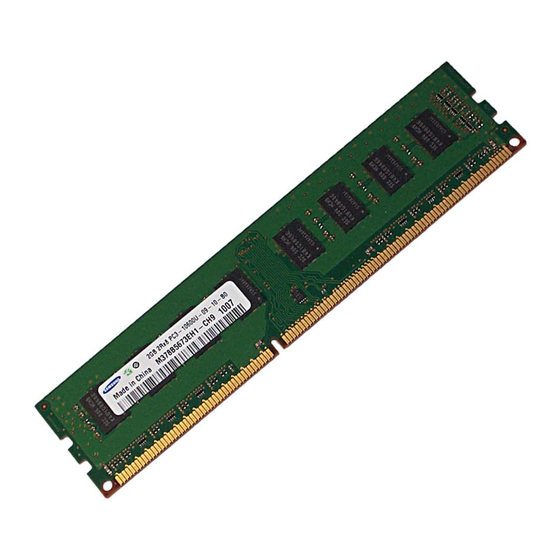
- Page 7 General Information DDR3 SDRAM 5. RDIMM RCD Information 1. RCD Identification in JEDEC Description in Module Label 2. Label Example 4GB 2Rx4 PC3 - 10600R - 09 - 10 - E1 - P0 M393B5170EH1-CH9 0849 Made in Korea 3. RCD Information...
- Page 8 General Information DDR3 SDRAM 78 + 4Ball FBGA for 1Gb D-die (x4/x8) 9.00 ± 0.10 0.80 x 10 = 8.00 #A1 INDEX MARK (Datum A) 0.80 1.60 4.00 9.00 ± 0.10 8 7 6 5 4 3 2 1 (Datum B) 0.35 ±...
- Page 9 General Information DDR3 SDRAM 78 Ball FBGA for 1Gb E-die (x4/x8) 7.50 ± 0.10 0.80 x 8 = 6.40 #A1 INDEX MARK (Datum A) 0.80 1.60 3.20 7.50 ± 0.10 8 7 6 5 4 3 2 1 (Datum B) 0.35 ±...
-
Page 10: Bottom View
General Information DDR3 SDRAM 78Ball FBGA for 2Gb B-die (x4/x8) 9.00 ± 0.10 #A1 INDEX MARK (Datum A) 0.80 1.60 3.60 9.00 ± 0.10 8 7 6 5 4 3 2 1 (Datum B) 0.35 ± 0.05 (0.95) 78 - ∅0.45 Solder ball MOLDING AREA (Post Reflow ∅0.50 ±... - Page 11 General Information DDR3 SDRAM x64/x72 240pin DDR3 SDRAM Unbuffered DIMM Units : Millimeters 133.35 128.95 (for x64) (for x72) 2.50 4.00 47.00 71.00 (for x64) (for x72) 1.270 ± 0.10 2x 2.10 ± 0.15 5.00 0.80 ± 0.05 3.80 0.2 ± 0.15 2.50...
- Page 12 General Information DDR3 SDRAM x64 204pin DDR3 SDRAM Unbuffered SODIMM Units : Millimeters 67.60 Max 3.8 1.00 ± 0.10 3.00 1.80 0.10 (OPTIONAL HOLES) 2X 4.00 ± 0.10 0.10 0.60 0.45 ± 0.03 4.00 ± 0.10 2.55 0.25 MAX 1.00 ± 0.10...
- Page 13 General Information DDR3 SDRAM x72 240pin DDR3 SDRAM Registered DIMM Units : Millimeters 133.35 131.35 128.95 4.00 max 9.76 10.9 18.92 32.40 18.93 9.74 30.00 1.0 max 2.50 1.27 ± 0.10 2x 2.10 ± 0.15 5.00 0.80 ± 0.05 3.80 0.2 ±...
-
Page 14: Front Part
General Information DDR3 SDRAM Registered DIMM Heat Spreader Design 1. FRONT PART Outside 133.15 ± 0.2 0.65 ± 0.2 130.45 ± 0.15 9.26 29.77 11.9 31.4 0.15 ± 0.12 Inside Green Line : TIM Attatch Line Reg. pedestal line 80.78 119.29... - Page 15 General Information DDR3 SDRAM 3. CLIP PART 39.3 ± Upper Bending Tilting Gap 29.77 0.1 ~ 0.3 4. DDR3 RDIMM ASS’Y View Reference thickness total (nominal) : Mono Package : 7.55mm, DDP Package 7.71mm (With Clip thickness) 132.95 133.45 ±...