
Related Manuals for Samsung DDR3


Summary of Contents for Samsung DDR3
- Page 1 General Information DDR3 SDRAM DDR3 SDRAM Product Guide October 2009 Memory Division October 2009...
-
Page 2: General Information
: Commercial Temp.( 0°C ~ 85°C) & Low Power : Commercial Temp.( 0°C ~ 85°C) & Low VDD(1.35V) 11. Speed : DDR3-800 : DDR3-1066 (533MHz @ CL=7, tRCD=7, tRP=7) : DDR3-1333 (667MHz @ CL=9, tRCD=9, tRP=9) : DDR3-1600 (800MHz @ CL=11, tRCD=11, tRP=11) DDR3 SDRAM Temp &... - Page 3 General Information 2. DDR3 SDRAM Component Product Guide Density Banks Part Number K4B1G0446D K4B1G0846D 1Gb D-die 8Banks K4B1G1646D K4B1G0446E K4B1G0846E 1Gb E-die 8Banks K4B1G1646E K4B1G0446E K4B1G0846E K4B1G0446F K4B1G0846F 1Gb F-die 8Banks K4B1G0446F K4B1G0846F K4B2G0446B K4B2G0846B 2Gb B-die 8Banks K4B2G1646B K4B2G0446B...
- Page 4 : Commercial Temp.( 0°C ~ 85°C) & Normal Power : Commercial Temp.( 0°C ~ 85°C) & Low VDD(1.35V) 12. Speed : DDR3-800 : DDR3-1066 (533MHz @ CL=7, tRCD=7, tRP=7) : DDR3-1333 (667MHz @ CL=9, tRCD=9, tRP=9) : DDR3-1600 (800MHz @ CL=11, tRCD=11, tRP=11) Note: PC3-6400(DDR3-800),PC3-8500(DDR3-1066),...
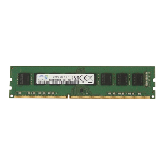
- Page 5 General Information 4. DDR3 SDRAM Module Product Guide 4.1 240Pin DDR3 Unbuffered DIMM (1.5V Product Org. Density Part Number Speed M378B2873DZ1 CF8/H9 128Mx 64 M378B2873EH1 CF8/H9/K0 M378B2873FHS CF8/H9 M391B2873DZ1 CF8/H9 128Mx 72 M391B2873EH1 CF8/H9/K0 M391B2873FH0 CF8/H9/K0 M378B5673DZ1 CF8/H9 M378B5673EH1 CF8/H9/K0...
- Page 6 General Information 4.3 204Pin DDR3 SoDIMM (1.5V Product) Org. Density Part Number Speed M471B2874DZ1 CF8/H9 M471B2873EH1 CF8/H9 128Mx 64 M471B2874EH1 CF8/H9 M471B2873FHS CF8/H9 M471B5673DZ1 CF8/H9 M471B5673EH1 CF8/H9 256Mx 64 M471B5673FH0 CF8/H9 M471B5773CHS CF8/H9 M471B5273BH1 CF8/H9 512Mx 64 M471B5273CH0 CF8/H9 4.4 204Pin DDR3 SoDIMM (1.35V Product) Org.
- Page 7 General Information 4.5 240Pin DDR3 Registered DIMM (1.5V Product) Org. Density Part Number Speed M393B2873DZ1 CF8/H9 128Mx 72 M393B2873EH1 CF8/H9 M393B2873FH0 CF8/H9 M393B5673DZ1 CF8/H9 M393B5673EH1 CF8/H9 M393B5673FH0 CF8/H9 256Mx 72 M393B5670DZ1 CF8/H9 M393B5670EH1 CF8/H9 M393B5670FH0 CF8/H9 M393B5173DZ1 CF7/F8 M393B5173EH1 CF7/F8...
- Page 8 General Information 4.6 240Pin DDR3 Registered DIMM (1.35V Product) Org. Density Part Number Speed M393B2873EH1 YF8/H9 128Mx 72 M393B2873FH0 YF8/H9 M393B5673EH1 YF8/H9 M393B5673FH0 YF8/H9 256Mx 72 M393B5670EH1 YF8/H9 M393B5670FH0 YF8/H9 M393B5773CH0 YF8/H9 M393B5173EH1 YF7/F8 M393B5173FH0 YF7/F8 M393B5170EH1 YF8/H9 M393B5170FH0 YF8/H9...
- Page 9 General Information 4.7 240Pin DDR3 VLP Registered DIMM (1.5V Product) Org. Density Part Number Speed M392B2873DZ1 CF8/H9 128Mx 72 M392B2873EH1 CF8/H9 M392B2873FH0 CF8/H9 M392B5673DZ1 CF8/H9 M392B5673EH1 CF8/H9 M392B5673FH0 CF8/H9 256Mx 72 M392B5670DZ1 CF8/H9 M392B5670EH1 CF8/H9 M392B5670FH0 CF8/H9 M392B5773CH0 CF8/H9 M392B5170DJ1...
- Page 10 General Information 4.8 240Pin DDR3 VLP Registered DIMM (1.35V Product) Org. Density Part Number Speed M392B2873EH1 YF8/H9 128Mx 72 M392B2873FH0 YF8/H9 M392B5673EH1 YF8/H9 M392B5673FH0 YF8/H9 256Mx 72 M392B5670EH1 YF8/H9 M392B5670FH0 YF8/H9 M392B5773CH0 YF8/H9 M392B5170EM1 YF8/H9 M392B5173FM0 YF7/F8 M392B5170FM0 YF8/H9 512Mx 72...
- Page 11 5.3 RCD Information - Example Voltage Vendor Revision Inphi GS04 B2 1.5V LV DDR3 B0 Inphi LV GS02 C0 1.35V LV DDR3 B0 4GB 2Rx4 PC3 - 10600R - 09 - 10 - E1 - P0 M393B5170EH1-CH9 Module P/N M393B5170EH1-CH9...
- Page 12 (Post Reflow ∅0.05 ± 0.05) (1.90) Bottom : Support Ball #A1 INDEX MARK MOLDING AREA #A1 INDEX MARK MOLDING AREA DDR3 SDRAM 9.00 ± 0.10 1.10 ± 0.10 9.00 ± 0.10 1.10 ± 0.10 October 2009 0.35 ± 0.05 0.35 ± 0.05...
- Page 13 96 - ∅0.45 Solder ball (Post Reflow ∅0.05 ± 0.05) (1.90) Bottom #A1 INDEX MARK MOLDING AREA #A1 INDEX MARK MOLDING AREA DDR3 SDRAM 7.50 ± 0.10 1.10 ± 0.10 7.50 ± 0.10 1.10 ± 0.10 October 2009 0.35 ± 0.05 0.35 ± 0.05...
-
Page 14: Bottom View
96 - ∅0.45 Solder ball (Post Reflow ∅0.50 ± 0.05) (1.90) BOTTOM VIEW #A1 INDEX MARK MOLDING AREA #A1 INDEX MARK MOLDING AREA DDR3 SDRAM 9.00 ± 0.10 TOP VIEW 9.00 ± 0.10 TOP VIEW October 2009 0.35 ± 0.05 1.10 ± 0.10 0.35 ±... - Page 15 (Datum B) 78 - ∅0.45 Solder ball (Post Reflow ∅0.50 ± 0.05) Bottom #A1 INDEX MARK 10.50 ± 0.10 #A1 INDEX MARK 9.00 ± 0.10 DDR3 SDRAM 0.35 ± 0.05 1.40 ± 0.10 0.35 ± 0.05 1.40 ± 0.10 October 2009...
- Page 16 0.80 1.60 3.20 8 7 6 5 4 3 2 1 (Datum B) 78 - ∅0.45 Solder ball (Post Reflow ∅0.50 ± 0.05) Bottom #A1 INDEX MARK 10.00 ± 0.10 DDR3 SDRAM 0.35 ± 0.05 1.40 ± 0.10 October 2009...
- Page 17 General Information x64/x72 240pin DDR3 SDRAM Unbuffered DIMM 2.50 54.675 47.00 5.00 1.50±0.10 2.50 Detail A 133.35 ± 0.15 128.95 (for x64) (for x72) 71.00 (for x64) (for x72) 0.80 ± 0.05 3.80 0.2 ± 0.15 1.00 Detail B DDR3 SDRAM Units : Millimeters Max 4.0...
- Page 18 General Information DDR3 SDRAM x64 204pin DDR3 SDRAM Unbuffered SODIMM Units : Millimeters 0.10 67.60 63.60 Max 3.8 1.00 ± 0.10 24.80 39.00 21.00 1.80 0.10 (OPTIONAL HOLES) 2X 4.00 ± 0.10 0.10 0.60 0.45 ± 0.03 1.65 4.00 ± 0.10 2.55...
- Page 19 General Information DDR3 SDRAM x72 240pin DDR3 SDRAM Registered DIMM Units : Millimeters 133.35 ± 0.15 128.95 Max 4.0 9.76 10.9 18.92 32.40 18.93 9.74 2.50 1.0 max 54.675 1.27 ± 0.10 47.00 71.00 5.00 0.80 ± 0.05 3.80 0.2 ± 0.15 10.9...
-
Page 20: Front Part
Green Line : TIM Attatch Line 80.78 119.29 2. BACK PART Outside Inside Green Line : TIM Attatch Line 133.15 ± 0.2 130.45 ± 0.15 29.77 31.4 ± 0.12 Reg. pedestal line 128.5 DDR3 SDRAM 0.65 ± 0.2 0.15 October 2009... - Page 21 General Information 3. CLIP PART 39.3 ± 29.77 4. DDR3 RDIMM ASS’Y View Reference thickness total (Maximum) : Mono Package : 7.55mm, DDP Package 7.71mm (With Clip thickness) * Dimension Index Min. E (Clip open size) Upper Bending Tilting Gap 0.1 ~ 0.3...