VIA Technologies VB7009 Mini-ITX Board Manuals
Manuals and User Guides for VIA Technologies VB7009 Mini-ITX Board. We have 2 VIA Technologies VB7009 Mini-ITX Board manuals available for free PDF download: User Manual
VIA Technologies VB7009 User Manual (129 pages)
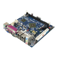
Mini-ITX embedded board
Brand: VIA Technologies
|
Category: Computer Hardware
|
Size: 4 MB
Table of Contents
-
Via C716
-
PS/2 Port24
-
VGA Port25
-
COM Port25
-
USB 2.0 Port28
-
Audio Jacks28
-
Jumpers47
-
PCI Slot58
-
Control Keys62
-
Getting Help62
-
Date65
-
Time65
-
Video65
-
Halt on65
-
IDE Channels66
-
CPU Feature70
-
PMON Support70
-
UMA Enable74
-
Panel Type74
-
Onchip SATA76
-
Hide D1F177
-
Eup/Erp Lot680
-
HPET Support81
-
WDRT Support81
-
WDRT Count81
-
DRAM Clock86
-
Amibios90
-
Processor90
-
System Time90
-
System Date90
-
Suspend Mode95
-
APM Settings96
-
Wake-Up Key97
-
System Time98
-
LAN Option ROM100
-
Boot Settings101
-
Quick Boot102
-
Quiet Boot102
-
Bootup Num-Lock102
-
Password Check103
-
DRAM Clock105
-
Panel Type106
-
Exit Options109
-
Discard Changes109
-
Vb7009-16116
-
Vb7009-10E119
-
Vb7009-12Xc121
-
Vb7009-12Qce124
Advertisement

VIA Technologies VB7009 User Manual (129 pages)
Mini-ITX embedded board
Brand: VIA Technologies
|
Category: Motherboard
|
Size: 3 MB
Table of Contents
-
PS/2 Port22
-
VGA Port23
-
COM Port24
-
USB 2.0 Port27
-
Audio Ports28
-
Jumpers47
-
PCI Slot58
-
Control Keys62
-
Getting Help63
-
Date66
-
Time66
-
Video66
-
Halt on66
-
IDE Channels67
-
CPU Feature71
-
PMON Support71
-
UMA Enable75
-
Panel Type75
-
Onchip SATA78
-
Hide D1F179
-
Eup/Erp Lot682
-
HPET Support83
-
WDRT Support83
-
WDRT Count83
-
DRAM Clock88
-
Amibios93
-
Processor93
-
System Time93
-
System Date93
-
APM Settings101
-
Boot Settings107
-
Exit Options114
-
Discard Changes114
-
Vb7009-16116
-
Vb7009-10E119
-
Vb7009-12Xc121
-
Vb7009-12Qce124