VIA Technologies VB7009 User Manual
Mini-itx embedded board
Hide thumbs
Also See for VB7009:
- User manual (124 pages) ,
- User manual (129 pages) ,
- User manual (117 pages)
Table of Contents
Advertisement
Quick Links
Advertisement
Table of Contents

Related Manuals for VIA Technologies VB7009


Summary of Contents for VIA Technologies VB7009
- Page 1 MANUAL USER VB7009 Mini-ITX embedded board 1.19-02232017-163900...
- Page 2 VIA Technologies, Inc. reserves the right the make changes to the products described in this manual at any time without prior notice. Regulatory Compliance FCC-A Radio Frequency Interference Statement This equipment has been tested and found to comply with the limits for a class A digital device, pursuant to part 15 of the FCC rules.
- Page 3 VB7009 User Manual Battery Recycling and Disposal Only use the appropriate battery specified for this product. Do not re-use, recharge, or reheat an old battery. Do not attempt to force open the battery. Do not discard used batteries with regular trash.
- Page 4 VB7009 User Manual Box Contents 1 x VB7009 board 1 x I/O bracket 1 x SATA cable Ordering Information Part Number Description VB7009-12QCE Mini-ITX Board with 1.2GHz VIA Eden ® X4 CPU with VGA, LVDS, 8 x USB 2.0, 6 x COM, 2 x Gigabit Ethernet, 2 x SATA, PCI slot, ATX connector ®...
-
Page 5: Table Of Contents
VB7009 User Manual Table of Contents 1. Product Overview ........................1 1.1. Key Features and Benefits ..........................1 ® ® ® ® 1.1.1. VIA C7 -D / C7 / Nano X2 E-Series / Eden X4 Processor ............1 1.1.2. VIA VX900 Chipset ............................ 1 1.1.3. - Page 6 Control Keys ..............................47 6.3. Navigating the BIOS Menus ...........................47 6.4. Getting Help ..............................47 6.5. Main Menu (BIOS for VB7009-16 / VB7009-10E / VB7009-12XC SKU) ..........48 6.5.1. Standard CMOS Features ........................48 6.5.2. Advanced BIOS Features ........................48 6.5.3. Advanced Chipset Features ........................48 6.5.4.
- Page 7 VB7009 User Manual 6.9.2. PMON support............................55 6.10. Hard Disk Boot Priority ...........................56 6.11. Advanced Chipset Features ...........................57 6.11.1. LCD Clock Source Control ........................57 6.11.2. LCD Backlight Control ..........................57 6.12. PCIE Bus Control ..............................58 6.12.1. PCIE Root Port ............................58 6.12.2. PCIE Target Link Speed ...........................58 6.12.3.
- Page 8 6.25. Load Optimized Defaults ..........................72 6.26. Set Supervisor/User Password ........................72 6.27. Save & Exit Setup .............................74 6.28. Exit Without Saving ............................74 6.29. Main Menu (BIOS for VB7009-12QCE SKU) ....................75 6.29.1. AMIBIOS ..............................75 6.29.2. Processor ..............................75 6.29.3. System Memory ............................75 6.29.4. System Time ..............................75 6.29.5.
- Page 9 VB7009 User Manual 6.30.5.1. Suspend Mode ..........................80 6.30.5.2. ACPI Version Features ........................80 6.30.5.3. USB S4 Wakeup ..........................80 6.30.6. APM Settings .............................81 6.30.6.1. Power Button Mode ........................81 6.30.6.2. Restore on AC/Power Loss ......................81 6.30.6.3. Resume on PS/2 KBC ........................82 6.30.6.4.
- Page 10 A.2. Installing the EMIO-1533 USB Wi-Fi Module ....................97 A.3. Installing the EMIO-5531 USB Wi-Fi + Bluetooth Module ...............99 Appendix B. Power Consumption Report .................. 101 B.1. VB7009-16 ................................101 B.1.1. System Idle – Windows 7 32-bit ......................101 B.1.2. S3 Status – Windows 7 Sleep ........................ 101 B.1.3.
- Page 11 VB7009 User Manual B.4.3. MP3 Playback – Windows Media Player10 ..................110 B.4.4. MP4 Playback –KM Player10........................110 B.4.5. Graphics – Run 3DMarks’06 ........................110 B.4.6. Functional Test – Run Passmark BurnIn test 6.0 ................. 111 B.4.7. Network Access <Dual LAN> – Gigabit Ethernet File Transmitting ..........111 B.4.8.
- Page 12 VB7009 User Manual Lists of Figures Figure 1: Layout diagram of the VB7009 mainboard (top view) ................6 Figure 2: Mounting holes and dimensions of the VB7009 mainboard ..............7 Figure 3: External I/O port dimensions of the VB7009 mainboard ................7 Figure 4: Height distribution of the VB7009 mainboard ....................8 Figure 5: External I/O ports ..............................9...
- Page 13 VB7009 User Manual Figure 47: Illustration of the Main menu screen (for VB7009-16/VB7009-10E/VB7009-12XC SKU) ....48 Figure 48: Illustration of the Standard CMOS Features screen ................50 Figure 49: Illustration of the IDE Channel 0 Master screen ..................51 Figure 50: Illustration of the IDE Channel 0 Slave screen ..................51 Figure 51: Illustration of the Advanced BIOS Features screen ................
- Page 14 VB7009 User Manual Figure 94: Connecting the USB Wi-Fi cable diagram ....................97 Figure 95: Installing Wi-Fi antenna cable diagram ...................... 98 Figure 96: Connecting Wi-Fi antenna cable to the EMIO-1533 module ............... 98 Figure 97: Installing EMIO-5531 USB Wi-Fi + BT module ..................99 Figure 98: Connecting the USB Wi-Fi cable diagram ....................
- Page 15 Table 32: LVDS panel power select jumper settings ....................38 Table 33: LVDS inverter power select jumper settings ..................... 39 Table 34: Serial port addresses and IRQs ........................78 Table 35: VB7009 mating connector vendor lists..................... 113 Downloaded from StockCheck.com...
-
Page 16: Product Overview
™ technology. The VIA VB7009 has one 1066MHz DDR3 DIMM slot that supports up to 4GB memory size. The VIA VB7009 provides support for high fidelity audio with its included VIA VT1708S High Definition Audio codec. In addition it supports two SATA 3Gbps storage devices. -
Page 17: Modular Expansion Options
The VIA VB7009 enables companies to slowly roll out upgrades as necessary instead of having to replace everything all at once. This ensures that companies using the VB7009 obtain the maximum benefits from its past investments in PCI expansion cards. -
Page 18: Product Specifications
1.0GHz VIA C7 ® (for VB7009-10E SKU Supports 400MHz Front Side Bus 1.2GHz VIA Nano ® X2 E-Series (for VB7009-12XC SKU Supports 800MHz Front Side Bus 1.2GHz VIA Eden ® X4 (for VB7009-12QCE SKU Supports 1066MHz Front Side Bus... - Page 19 1 x System fan connector 3 x COM pin headers by F81865-I, with 5V/12V select (available only for VB7009-16 & VB7009- 10E SKU) 5 x COM pin headers by F81865-I, with 5V/12V select (available only for VB7009-12XC & VB7009- ...
- Page 20 RoHS Notes: 1. The VB7009-16 and VB7009-12XC SKUs use heatsink with fan. 2. The VB7009-10E and VB7009-12QCE SKUs use heatsink. 3. As the operating temperature provided in the specifications is a result of the test performed in VIA’s chamber, a number of variables can influence this result. Please note that the working temperature may vary depending on the actual situation and environment.
-
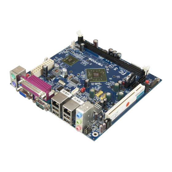
Page 21: Layout Diagram
CMOS battery slot Front panel pin header SATA connectors Figure 1: Layout diagram of the VB7009 mainboard (top view) Note: The additional COM pin headers labeled as “COM5” and “COM6” are available only in VB7009-12XC & VB7009-12QCE SKU. Downloaded from StockCheck.com... -
Page 22: Product Dimensions
7.92 mm 10.16 mm 33.02 mm 39.37 mm 170.00 mm 4.97 mm 6.17 mm 6.35 mm Figure 2: Mounting holes and dimensions of the VB7009 mainboard 31.50 mm 25.55 mm 21.75 mm 19.00 mm 6.25 mm 6.50 mm 6.50 mm 0.00... -
Page 23: Height Distribution
VB7009 User Manual 1.5. Height Distribution Height: 38.50 mm Height: 32.00 mm Height: 33.00 mm Height: 35.00 mm Height: 34.60 mm Figure 4: Height distribution of the VB7009 mainboard Downloaded from StockCheck.com... -
Page 24: I/O Interface
VB7009 User Manual 2. I/O Interface The VIA VB7009 has a wide selection of interfaces integrated into the board. It includes a selection of frequently used ports as part of the external I/O coastline. 2.1. External I/O Ports PS2 Mouse port... -
Page 25: Vga Port
VB7009 User Manual 2.1.2. VGA Port The integrated 15-pin VGA port uses a female DE-15 connector. The VGA port is for connecting to analog displays. The pinout of the VGA port is shown below. Figure 7: VGA port diagram Signal... -
Page 26: Parallel Port
VB7009 User Manual 2.1.4. Parallel Port The integrated 25-pin parallel port uses a female DB-25 connector. A parallel port is a standard printer port that supports Enhanced Parallel Port (EPP) and Extended Capabilities Parallel Port (ECP) modes. The pinout of the Parallel port is shown below. -
Page 27: Gigabit Ethernet Port
VB7009 User Manual 2.1.5. Gigabit Ethernet Port The two integrated 8-pin Gigabit Ethernet ports are using an 8 Position 8 Contact (8P8C) receptacle connector (commonly referred to as RJ-45). The Gigabit Ethernet ports are controlled by VIA Gigabit Ethernet controller. The pinout of the Gigabit Ethernet port is shown below. -
Page 28: Usb 2.0 Port
VB7009 User Manual 2.1.6. USB 2.0 Port There are four integrated USB 2.0 ports located below the two Gigabit Ethernet ports at the external I/O panel. The USB 2.0 interface port gives complete Plug and Play and hot swap capability for external devices and it complies with USB UHCI, rev. -
Page 29: Onboard Connectors
VB7009 User Manual 2.2. Onboard Connectors 2.2.1. ATX Power Connector The mainboard has a 20-pin ATX power connector onboard. The ATX power connector is labeled as “ATX_POWER1”. The pinout of the ATX power connector is shown below. Figure 13: ATX power connector diagram... -
Page 30: Cmos Battery Slot
VB7009 User Manual 2.2.2. CMOS Battery Slot The mainboard is equipped with a CMOS battery slot, which is compatible with CR2032 coin batteries. The CMOS battery slot is labeled as “BAT2”. When inserting a CR2032 coin battery, be sure that the positive side is facing the locking clip. -
Page 31: Front Panel Pin Header
VB7009 User Manual 2.2.3. Front Panel Pin Header The front panel pin header consists of 15 pins in a 16-pin block. Pin 15 is keyed. The front panel pin header is labeled as “F_PANEL1”. It provides access to system LEDs, power, reset, system speaker and HDD LED. -
Page 32: Front Audio Pin Header
VB7009 User Manual 2.2.4. Front Audio Pin Header In addition to the TRS audio jacks on the external I/O coastline, the mainboard has a pin header for Line- out and Mic-in. The pin header is labeled as “F_AUDIO1”. The pinout of the pin header is shown below. -
Page 33: Smbus Pin Header
VB7009 User Manual 2.2.5. SMBus Pin Header The SMBus pin header consists of three pins that allow connecting the SMBus devices. Devices communicate with a SMBus host and/or other SMBus devices using the SMBus interface. It is labeled as “SMBUS1”. The pinout of the SMBus pin header is shown below. -
Page 34: Cpu And System Fan Connectors
VB7009 User Manual 2.2.6. CPU and System Fan Connectors There are two fan connectors on board: one for the CPU and one for the chassis. The fan connector for the CPU is labeled as “CPUFAN1” and the fan connector for the system is labeled as “SYSFAN1”. The fans provide variable fan speeds controlled by the BIOS. -
Page 35: Sata Connectors
VB7009 User Manual 2.2.7. SATA Connectors The two SATA connectors on board can support up to 3 Gbps transfer speeds, enabling fast data file transfer with independent DMA operation. The SATA connectors are labeled as “SATA1” and “SATA2”. The pinout of the SATA connectors are as shown below. -
Page 36: Usb 2.0 Pin Headers
VB7009 User Manual 2.2.8. USB 2.0 Pin Headers The mainboard has two USB 2.0 pin headers blocks that support up to four USB 2.0 ports. The pin header blocks are labeled as USB_4, and “USB_5”. The pinout of the USB pin headers are shown below. -
Page 37: Com Pin Headers
COM pin header supports the RS-232 standard. The COM pin headers labeled as “COM2, COM3 and COM4” are available in VB7009-16 and VB7009-10E SKUs, while the additional “COM5” and “COM6” pin headers are offered only by VB7009-12XC and VB7009-12QCE SKUs. All the COM pin headers can support +5V or +12V. -
Page 38: Ps/2 Keyboard And Mouse Pin Header
VB7009 User Manual 2.2.10. PS/2 Keyboard and Mouse Pin Header The mainboard has a pin header for PS/2 keyboard and mouse. The pin header is labeled as “JKB/MS1”. The pinout of the pin header is shown below. Figure 22: PS/2 keyboard and mouse pin header diagram... -
Page 39: Lvds Panel Connector
VB7009 User Manual 2.2.11. LVDS Panel Connector The mainboard has one 40-pin LVDS panel connector on the bottom side. It can support one dual- channel LVDS or one single-channel LVDS. The LVDS panel connector is labeled as “PANEL_CONN1”. The pinout of the connector is shown below. -
Page 40: Table 20: Lvds Panel Connector Pinout (Single-Channel)
VB7009 User Manual Signal Signal PVDD PVDD -A0_L A0_L -A1_L A1_L -A2_L A2_L -CLK1_L CLK1_L -A3_L A3_L SPCLK1 SPD1 Table 20: LVDS panel connector pinout (single-channel) Downloaded from StockCheck.com... -
Page 41: Lvds Inverter Connector
VB7009 User Manual 2.2.12. LVDS Inverter Connector The mainboard has one LVDS Inverter connector on the bottom side. The LVDS Inverter connector is labeled as “INVERTER1”. The pinout of the connector is shown below. Figure 24: LVDS Inverter connector diagram... -
Page 42: S/Pdif Connector
VB7009 User Manual 2.2.13. S/PDIF Connector The mainboard has one 3-pin S/PDIF (Sony/Philips Digital Interface Format) connector. The S/PDIF output provides digital audio to external speakers or compressed AC3 data to an external Dolby Digital Decoder. The connector is labeled as “S/PDIF”. The pinout of the connector is shown below. -
Page 43: Spi Pin Header
VB7009 User Manual 2.2.14. SPI Pin Header The mainboard has one 8-pin SPI pin header. The SPI (Serial Peripheral Interface) pin-header is used to connect to the SPI BIOS programming fixture. The pin header is labeled as “SPI1”. The pinout of the pin header is shown below. -
Page 44: Lpc Pin Header
VB7009 User Manual 2.2.15. LPC Pin Header The mainboard has one LPC pin header for connecting LPC devices. The pin header is labeled as “LPC1”. The pinout of the pin header is shown below. Figure 27: LPC pin header diagram... -
Page 45: Digital I/O Pin Header
VB7009 User Manual 2.2.16. Digital I/O Pin Header The onboard Digital I/O pin header supports up to four GPO and four GPI signals. The pin header is labeled as “DIO1”. The pinout of the pin headers are shown below. Figure 28: Digital I/O pin header diagram... -
Page 46: Temperature Sensor Pin Header
VB7009 User Manual 2.2.17. Temperature Sensor Pin Header The mainboard supports a pin header (3-pin) that allows the connection of a temperature sensor cable for detecting the system’s internal air temperature. The temperature reading can be seen in the BIOS Setup Utility. -
Page 47: Jumpers
VB7009 User Manual 3. Jumpers Jumper Description A jumper consists of pair conductive pins used to close in or bypass an electronic circuit to set up or configure particular feature using a jumper cap. The jumper cap is a small metal clip covered by plastic. It performs like a connecting bridge to short (connect) the pair of pins. -
Page 48: Clear Cmos Jumper
VB7009 User Manual 3.1. Clear CMOS Jumper The onboard CMOS RAM stores system configuration data and has an onboard battery power supply. To reset the CMOS settings, set the jumper on pins 2 and 3 while the system is off. Return the jumper to pins 1 and 2 afterwards. -
Page 49: Com Voltage Select Jumpers
VB7009 User Manual 3.2. COM Voltage Select Jumpers Each of the additional COM ports (available through the onboard COM pin headers, see page 22) can support both +5V and +12V. COM2 has its own pin header block. COM3 and COM4 share a single pin header block. -
Page 50: Com3 And Com4 Voltage Select Jumper
VB7009 User Manual 3.2.2. COM3 and COM4 Voltage Select Jumper The voltage for COM3 and COM4 is controlled by the jumper labeled as “J13”. Refer to Figure 33 for the location of the jumper. The voltage can be either +5V or +12V. +5V is the default setting. The even pin numbers correspond to COM3. -
Page 51: Com5 And Com6 Voltage Select Jumper
VB7009 User Manual 3.2.3. COM5 and COM6 Voltage Select Jumper The voltage for COM5 and COM6 is controlled by the jumper labeled as “J14”. Refer to Figure 34 for the location of the jumper. The voltage can be either +5V or +12V. +5V is the default setting. The even pin numbers correspond to COM5. -
Page 52: Sata Dom Voltage Select Jumper
VB7009 User Manual 3.3. SATA DOM Voltage Select Jumper The SATA connectors (see page 20) can be used to support Disk-on-Module (DOM) flash drives. When the jumpers are set, +5V will be delivered to the 7 pin of the SATA connectors. The pin jumper is labeled as “J2”. -
Page 53: Lvds Panel Power Select Jumper
VB7009 User Manual 3.4. LVDS Panel Power Select Jumper The mainboard has a jumper that controls the voltage delivered to the LVDS panel connector. The jumper is labeled as “PVDD1”. The jumper settings are shown below. Figure 36: LVDS panel power select jumper diagram... -
Page 54: Lvds Inverter Power Select Jumper
VB7009 User Manual 3.5. LVDS Inverter Power Select Jumper The mainboard has a jumper that controls the input voltage delivered to the LVDS inverter connector. The jumper is labeled as “IVDD_SEL1”. The jumper settings are shown below. Figure 37: LVDS inverter power select jumper diagram... -
Page 55: Expansion Slots
VB7009 User Manual 4. Expansion Slots 4.1. DDR3 Memory Slots The mainboard provide one DDR3 DIMM memory slot. The memory slot can accommodate up to 4GB of 1066MHz memory. The memory slot is labeled as “DIMM1”. The location of the DDR3 memory slot is shown below. -
Page 56: Installing A Memory Module
VB7009 User Manual 4.1.1. Installing a Memory Module Step 1 Disengage the locking mechanism at both ends of the DIMM slot by pressing the retaining clips outward. Figure 39: Unlocking the memory DIMM slot Step 2 Align the notch on the DIMM memory module with the counterpart on the DIMM slot. -
Page 57: Removing A Memory Module
VB7009 User Manual 4.1.2. Removing a Memory Module Step 1 To disengage the locking clips, push outward the locking clips on both ends of memory slot. When the locking clips have cleared, the DIMM memory module will automatically pop up. Remove the memory module. -
Page 58: Pci Slot
VB7009 User Manual 4.1.3. PCI Slot The onboard PCI slot, labeled as “PCI_SLOT1”, supports 5V 32-bit PCI cards. It is not compatible with PCI cards requiring 3.3V signaling. The location of the PCI slot is shown below. key notch Figure 43: PCI slot diagram Notes: 1. -
Page 59: Installing Into A Chassis
VB7009 User Manual 5. Installing into a Chassis The VB7009 can be fitted into any chassis that has the mounting holes for compatible with the standard Mini-ITX mounting hole locations. Additionally, the chassis must meet the minimum height requirements for specified areas of the mainboard. If a riser card module is being used, the chassis will need to accommodate the additional space requirements. -
Page 60: Suggested Minimum Chassis Height
VB7009 User Manual 5.1.2. Suggested minimum chassis height The figure below shows the suggested minimum height requirements for the internal space of the chassis. It is not necessary for the internal ceiling to be evenly flat. What is required is that the internal ceiling height must be strictly observed for each section that is highlighted. -
Page 61: Suggested Keepout Areas
VB7009 User Manual 5.1.3. Suggested keepout areas The figure below shows the areas of the mainboard that is highly suggested to leave unobstructed. Keep out area Figure 46: Suggested keepout areas Downloaded from StockCheck.com... -
Page 62: Bios Setup Utility
VB7009 User Manual 6. BIOS Setup Utility 6.1. Entering the BIOS Setup Utility Power on the computer and press Delete during the beginning of the boot sequence to enter the BIOS Setup Utility. If the entry point has passed, restart the system and try again. -
Page 63: Main Menu (Bios For Vb7009-16 / Vb7009-10E / Vb7009-12Xc Sku)
: Select Item F10: Save & Exit Setup Time, Date, Hard Disk Type... Figure 47: Illustration of the Main menu screen (for VB7009-16/VB7009-10E/VB7009-12XC SKU) 6.5.1. Standard CMOS Features Use this menu to set basic system configurations. 6.5.2. Advanced BIOS Features Use this menu to set the advanced features available on your system. -
Page 64: Frequency/Voltage Control
VB7009 User Manual 6.5.8. Frequency/Voltage Control Use this menu to set the system frequency and voltage control. 6.5.9. Load Optimized Defaults Use this menu option to load BIOS default settings for optimal and high performance system operations. 6.5.10. Set Supervisor Password Use this menu option to set the BIOS supervisor password. -
Page 65: Standard Cmos Features
VB7009 User Manual 6.6. Standard CMOS Features Phoenix - AwardBIOS CMOS Setup Utility Standard CMOS Features Item Help Date (mm:dd:yy) Mon, Sept 26 2011 Time (hh:mm:ss) 3 : 17 : 8 Menu Level IDE Channel 0 Master [None] IDE Channel 0 Slave... -
Page 66: Ide Channels
VB7009 User Manual 6.7. IDE Channels Channel 0 Master Phoenix - AwardBIOS CMOS Setup Utility IDE Channel 0 Master Item Help IDE HDD Auto-Detection [Press Enter] Menu Level IDE Channel 0 Master [Auto] Access Mode [Auto] To auto-detect the HDD's size, head... - Page 67 VB7009 User Manual The specifications of your drive must match with the drive table. The hard disk will not work properly if you enter incorrect information in this category. Select “Auto” whenever possible. If you select “Manual”, make sure the information is from your hard disk vendor or system manufacturer.
-
Page 68: Advanced Bios Features
VB7009 User Manual 6.8. Advanced BIOS Features Phoenix - AwardBIOS CMOS Setup Utility Advanced BIOS Features CPU Feature [Press Enter] Item Help Hard Disk Boot Priority [Press Enter] Quick Power On Self Test [Enabled] First Boot Device [None] Menu Level... -
Page 69: Boot Other Device
VB7009 User Manual 6.8.3. Boot Other Device Enables the system to boot from alternate devices if the system fails to boot from the “First/Second/Third Boot Device” lists. Settings Description Disabled No alternate boot device allowed Enabled Enable alternate boot device 6.8.4. -
Page 70: Cpu Feature
VB7009 User Manual 6.9. CPU Feature Phoenix - AwardBIOS CMOS Setup Utility CPU Features Item Help Thermal Management [Thermal Monitor 3] PMON support [Disabled] Menu Level Thermal Monitor 3 Dynamic Ratio & VID transition : Move Enter: Select +/-/PU/PD: Value... -
Page 71: Hard Disk Boot Priority
VB7009 User Manual 6.10. Hard Disk Boot Priority Phoenix - AwardBIOS CMOS Setup Utility Hard Disk Boot Priority Item Help 1. Bootable Add-in Cards Menu Level Use < > or < > to select a device, then press < + > to move it up, or <... -
Page 72: Advanced Chipset Features
VB7009 User Manual 6.11. Advanced Chipset Features Phoenix - AwardBIOS CMOS Setup Utility Advanced Chipset Features Item Help PCIE Bus Control [Press Enter] UMA & P2P Bridge Control [Press Enter] CPU & PCI Bus Control [Press Enter] Menu Level LCD Clock Source Control... -
Page 73: Pcie Bus Control
VB7009 User Manual 6.12. PCIE Bus Control Phoenix - AwardBIOS CMOS Setup Utility PCIE Bus Control PCIE Root Port [Enable] Item Help PCIE Target Link Speed [Auto] PCIE PE0 Control [Enable] PCIE Hot-Reset Enable [Disabled] Menu Level PCIE Root-Port-Reset Enable... -
Page 74: Uma & P2P Bridge Control
VB7009 User Manual 6.13. UMA & P2P Bridge Control Phoenix - AwardBIOS CMOS Setup Utility UMA & P2P Bridge Control UMA Enable [Enable] Item Help VGA Share Memory Size [256M] CPU Direct Access FB [Enable] Select Display Device [Manual] Menu Level... -
Page 75: Cpu & Pci Bus Control
VB7009 User Manual 6.14. CPU & PCI Bus Control Phoenix - AwardBIOS CMOS Setup Utility CPU & PCI Bus Control Item Help PCI Master 0 WS Write [Enabled] PCI Delay Transaction [Enabled] SB P2P Bridge [Disabled] Menu Level : Move... -
Page 76: Integrated Peripherals
VB7009 User Manual 6.15. Integrated Peripherals Phoenix - AwardBIOS CMOS Setup Utility Integrated Peripherals Item Help VIA OnChip IDE Device [Press Enter] VIA OnChip PCI Device [Press Enter] SuperIO Device [Press Enter] Menu Level USB Device Setting [Press Enter] : Move... -
Page 77: Via Onchip Pci Device
VB7009 User Manual 6.17. VIA OnChip PCI Device Phoenix - AwardBIOS CMOS Setup Utility VIA OnChip PCI Device Item Help Onboard PCIE LAN [Enabled] Hide D1F1 [Disabled] OnChip HDAC Device [Enabled] Menu Level Clear HDA Wake Enable bit [Enabled] NB HD Audio Codec 1... -
Page 78: Superio Device
VB7009 User Manual 6.18. SuperIO Device Phoenix - AwardBIOS CMOS Setup Utility SuperIO Device Item Help Onboard Serial Port 1 [3F8/IRQ4] Onboard Serial Port 2 [2F8/IRQ3] Onboard Serial Port 3 [3E8/IRQ4] Menu Level Onboard Serial Port 4 [2E8/IRQ4] Onboard Parallel Port... -
Page 79: Usb Device Setting
VB7009 User Manual 6.19. USB Device Setting Phoenix - AwardBIOS CMOS Setup Utility USB Device Setting Item Help USB 1.0 Controller [Enabled] USB 2.0 Controller [Enabled] USB Operation Mode [High Speed] Menu Level USB Keyboard Function [Enabled] USB Mouse Function... -
Page 80: Power Management Setup
VB7009 User Manual 6.20. Power Management Setup Phoenix - AwardBIOS CMOS Setup Utility Power Management Setup Item Help EuP/ErP Lot6 [Disabled] ACPI Suspend Type [S1&S3] Soft-Off by PWRBTN [Instant-Off] Menu Level Run VGABIOS if S3 Resume [Auto] AC Loss Auto Restart... -
Page 81: Run Vgabios If S3 Resume
VB7009 User Manual 6.20.4. Run VGABIOS if S3 Resume Select whether to run VGA BIOS if resuming from S3 state. This is only necessary for older VGA drivers. Settings: [Auto, Yes, No] 6.20.5. AC Loss Auto Restart The field defines how the system will respond after an AC power loss during system operation. -
Page 82: Wakeup Event Detect
VB7009 User Manual 6.21. Wakeup Event Detect Phoenix - AwardBIOS CMOS Setup Utility Wakeup Event Detect Item Help PS2KB Wakeup Select [Hot Key] PS2KB Wakeup Key Select [Any Key] PS2MS Wakeup Key Select [Any Button] Menu Level PS2 Keyboard Power ON... -
Page 83: Resume Time (Hh:mm:ss)
VB7009 User Manual 6.21.8. Resume Time (hh:mm:ss) This field can only be set if “RTC Alarm Resume” is enabled. The field specifies the time for “RTC Alarm Resume”. Downloaded from StockCheck.com... -
Page 84: Pnp/Pci Configurations
VB7009 User Manual 6.22. PnP/PCI Configurations Phoenix - AwardBIOS CMOS Setup Utility PnP/PCI Configurations Item Help Init Display First [PCIEx] Resources Controlled By [Auto(ESCD)] Menu Level IRQ Resources Press Enter : Move Enter: Select +/-/PU/PD: Value F10: Save ESC: Exit... -
Page 85: Pc Health Status
VB7009 User Manual 6.23. PC Health Status Phoenix - AwardBIOS CMOS Setup Utility PC Health Status Item Help VCore 1.000V +3.3V 3.200V 5.100V Menu Level +12V 11.880V SYSTEM Temp. 30°C CPU FAN 0 RPM System FAN 0 RPM : Move... -
Page 86: Frequency/Voltage Control
VB7009 User Manual 6.24. Frequency/Voltage Control Phoenix - AwardBIOS CMOS Setup Utility Frequency/Voltage Control Current FSB Frequency 100 MHz Item Help Current DRAM Frequency 533 MHz DRAM Clock [By SPD] Menu Level Spread Spectrum [+/-0.1%] : Move Enter: Select +/-/PU/PD: Value... -
Page 87: Load Optimized Defaults
VB7009 User Manual 6.25. Load Optimized Defaults Phoenix - AwardBIOS CMOS Setup Utility Standard CMOS Features Frequency/Voltage Control Advanced BIOS Features Load Optimized Defaults Advanced Chipset Features Set Supervisor Password Integrated Peripherals Set User Password Load Optimized Defaults (Y/N)? N Power Management Setup Save &... - Page 88 VB7009 User Manual There are two types of passwords you can set: Supervisor password and User password. When a supervisor password is used, the BIOS Setup program can be accessed and the BIOS settings can be changed. When a user password is used, the BIOS Setup program can be accessed but the BIOS settings cannot be changed.
-
Page 89: Save & Exit Setup
VB7009 User Manual 6.27. Save & Exit Setup Phoenix - AwardBIOS CMOS Setup Utility Standard CMOS Features Frequency/Voltage Control Advanced BIOS Features Load Optimized Defaults Advanced Chipset Features Set Supervisor Password Integrated Peripherals Set User Password SAVE to CMOS and EXIT (Y/N)? Y Power Management Setup Save &... -
Page 90: Main Menu (Bios For Vb7009-12Qce Sku)
The System Overview screen is the default screen that is shown when the BIOS Setup Utility is launched. This screen can be accessed by traversing the navigation bar to the “Main” label. Figure 72: Illustration of the Main menu screen (for VB7009-12QCE SKU) 6.29.1. AMIBIOS The content in this section of the screen shows the current BIOS version, build date, and ID number. -
Page 91: Advanced Settings
VB7009 User Manual 6.30. Advanced Settings The Advanced Settings screen shows a list of categories that can provide access to a sub-screen. Sub- screen links can be identified by the preceding right-facing arrowhead. Figure 73: Illustration of the Advanced Settings screen... -
Page 92: Ide Configuration
VB7009 User Manual Figure 74: Illustration of the CPU Configuration screen 6.30.2. IDE Configuration The IDE Configuration screen shows links to the primary master and slave IDE hard drive information screens. Figure 75: Illustration of IDE Configuration screen 6.30.3. SuperIO Configuration The SuperIO Configuration screen shows the specific addresses and IRQs of the onboard serial ports. -
Page 93: Serial Ports 1 To 6 Address
VB7009 User Manual Figure 76: Illustration of SuperIO Configuration screen 6.30.3.1. Serial Ports 1 to 6 Address The Serial Port 1 to 6 has three selectable options. Port Address and IRQs 3F8/IRQ4/Disabled 2F8/IRQ4/Disabled 3E8/IRQ4/Disabled 2E8/IRQ4/Disabled 2B0/IRQ4/Disabled 2B8/IRQ4/Disabled Table 34: Serial port addresses and IRQs 6.30.3.2. -
Page 94: Hardware Health Configuration
VB7009 User Manual 6.30.4. Hardware Health Configuration The Hardware Health Configuration screen has no editable fields. The system temperature is taken from an optional sensor that is connected to the J5 pin header. Figure 77: Illustration of Hardware Health Configuration screen 6.30.4.1. -
Page 95: Acpi Settings
VB7009 User Manual 6.30.5. ACPI Settings ACPI grants the operating system direct control over system power management. The ACPI Configuration screen can be used to set a number of power management related functions. Figure 78: Illustration of ACPI Configuration screen 6.30.5.1. -
Page 96: Apm Settings
VB7009 User Manual 6.30.6. APM Settings APM enables the operating system to co-work with the BIOS to control the system power management. The APM Configuration screen can be used to set a number of power management functions. Figure 79: Illustration of APM Configuration screen 6.30.6.1. -
Page 97: Resume On Ps/2 Kbc
VB7009 User Manual 6.30.6.3. Resume on PS/2 KBC Resume on PS/2 KBC wakes up a system that has been put into suspend or standby mode. When this feature is enabled, keyboard activity as defined in the Wake-Up Key feature will cause the system to wake up. -
Page 98: Resume On Rtc Alarm
VB7009 User Manual 6.30.6.8. Resume on RTC Alarm Resume on RTC Alarm can only be used if Resume on Software RTC Alarm is not enabled. This feature enables the BIOS to automatically power on the system at a scheduled time. When enabled, the RTC Alarm Date and System Time features will be unlocked. -
Page 99: Usb Configuration
VB7009 User Manual 6.30.8. USB Configuration The USB Configuration screen shows the number of connected USB devices. Figure 81: Illustration of USB Configuration screen 6.30.8.1. Legacy USB Support The Legacy USB Support feature enables environments that do not have native USB support to use USB devices. -
Page 100: Crb Configuration
VB7009 User Manual 6.30.9. CRB Configuration The CRB Configuration screen shows the available BIOS-controlled DRAM clock, graphics adapter, display device and LAN control features. Figure 82: Illustration of CRB Configuration screen 6.30.9.1. VT6130 LAN Control The VT6130 LAN Control feature determines whether the onboard LAN controller will be used or not. -
Page 101: Boot Settings
VB7009 User Manual 6.31. Boot Settings The Boot Settings screen has a single link that goes to the Boot Settings Configuration screen. Figure 83: Illustration of Boot Settings screen 6.31.1. Boot Settings Configuration The Boot Settings Configuration screen has several features that can be run during the system boot sequence. -
Page 102: Quick Boot
VB7009 User Manual 6.31.1.1. Quick Boot The Quick Boot feature enables the BIOS to skip certain tests in order to speed up the boot sequence. This feature has two options: enabled and disabled. 6.31.1.2. Quiet Boot The Quiet Boot feature hides all of the Power-on Self Test (POST) messages during the boot sequence. -
Page 103: Security Settings
VB7009 User Manual 6.32. Security Settings The Security Settings screen provides a way to restrict access to the BIOS or even the entire system. Figure 85: Illustration of Security Settings screen 6.32.1. Security Settings 6.32.1.1. Change Supervisor Password This option is for setting a password for accessing the BIOS setup utility. When a password has been set, a password prompt will be displayed whenever the BIOS setup utility is launched. -
Page 104: Advanced Chipset Settings
VB7009 User Manual 6.33. Advanced Chipset Settings The Advanced Chipset Settings screen has two links for accessing North and South bridge functions. Though the VX900 is a single chip solution, the North and South bridge categories are still for grouping features. -
Page 105: Dram Clock/Timing Configuration
VB7009 User Manual 6.33.1.1. DRAM Clock/Timing Configuration The DRAM Clock/Timing Configuration screen has one feature for controlling the system DRAM. All other DRAM features are automated and cannot be accessed. Figure 88: Illustration of DRAM Frequency/Timing Configuration screen 6.33.1.1.1. DRAM Clock The DRAM Clock option enables the user to determine how the BIOS handles the memory clock frequency. -
Page 106: Onchip Vga Configuration
VB7009 User Manual 6.33.1.2. OnChip VGA Configuration The OnChip VGA Configuration screen has features for controlling the integrated graphics controller in the VX900 chipset. Figure 89: Illustration of OnChip VGA Configuration screen 6.33.1.2.1. Select Display Device 1 and 2 The Select Display Device feature enables the user to choose a specific display interface. This feature has two options: CRT and LCD. -
Page 107: Cpu Direct Access Frame Buffer
VB7009 User Manual 6.33.1.2.4. CPU Direct Access Frame Buffer The CPU Direct Access Frame Buffer feature enables the CPU to write to the portion of memory reserved for the integrated graphics controller. This feature has two options: “Disabled” and “Enabled”. -
Page 108: South Bridge Via Vx900 Configuration
VB7009 User Manual 6.33.2. South Bridge VIA VX900 Configuration The South Bridge VIA VX900 Configuration screen has the following features. Figure 90: Illustration of South Bridge VIA VX900 Configuration screen 6.33.2.1. OnChip HDAC Device The OnChip HDAC Device feature enables the BIOS to control the high definition audio codec in the chipset. -
Page 109: Exit Options
VB7009 User Manual 6.34. Exit Options Figure 91: Illustration of Exit Options screen 6.34.1. Save Changes and Exit Save all changes to the BIOS and exit the BIOS Setup Utility. The “F10” hotkey can also be used to trigger this command. -
Page 110: Driver Installation
7. Driver Installation 7.1 Microsoft Driver Support The VIA VB7009 mainboard is compatible with Microsoft operating systems. The latest Windows drivers can be downloaded from the VIA website at http://www.viatech.com/en/. For embedded operating systems, the related drivers can be found in the VIA website at http://www.viatech.com/en/. -
Page 111: Appendix A. Installing Wireless Accessories
VB7009 User Manual Appendix A. Installing Wireless Accessories The section provides the installation of the optional wireless accessories for the VB7009 mainboard. A.1. Installing the VNT9271 USB Wi-Fi Dongle Step 1 Locate a USB 2.0 port on the back panel I/O. -
Page 112: Installing The Emio-1533 Usb Wi-Fi Module
Connect one end of USB Wi-Fi cable to pin 1, 3, 5, and 7 of onboard USB 2.0 pin header (USB_4 or USB_5) on VB7009 board, and then connect the other end of the cable to the EMIO-1533 module. Figure 94: Connecting the USB Wi-Fi cable diagram... -
Page 113: Figure 95: Installing Wi-Fi Antenna Cable Diagram
VB7009 User Manual Step 3 Insert the Wi-Fi antenna cable into the antenna hole from the inside of the panel I/O plate. Insert the toothed washer, fasten it with the nut and install the external antenna. P a n e l I... -
Page 114: Installing The Emio-5531 Usb Wi-Fi + Bluetooth Module
Connect one end of USB Wi-Fi cable to pin 1, 3, 5, and 7 of onboard USB 2.0 pin header (USB_4 or USB_5) on VB7009 board, and then connect the other end of the cable to the EMIO-5531 module. Figure 98: Connecting the USB Wi-Fi cable diagram... -
Page 115: Figure 99: Installing Wi-Fi Antenna Cable Diagram
VB7009 User Manual Step 3 Insert the Wi-Fi antenna cable into the antenna hole from the inside of the panel I/O plate. Insert the toothed washer, fasten it with the nut and install the external antenna. P a n e l I... -
Page 116: Appendix B. Power Consumption Report
VB7009 User Manual Appendix B. Power Consumption Report Power consumption tests were performed on the VIA VB7009. The following tables represent the breakdown of the voltage, amp and wattage values while running common system applications. B.1. VB7009-16 The tests were performed based on the following additional components: ®... -
Page 117: Mp3 Playback - Windows Media Player10
VB7009 User Manual B.1.3. MP3 Playback – Windows Media Player10 Power Plane Volts Amperes Watts +3.3V 3.192 0.680 2.171 4.917 2.240 11.014 +5VSB 5.104 0.057 0.291 +12V 11.998 0.086 1.032 Total Power 14.508 Consumption B.1.4. DVD Playback – PowerDVD 8.0... -
Page 118: Network Access
VB7009 User Manual B.1.7. Network Access <Single LAN> – Gigabit Ethernet File Transmitting Power Plane Volts Amperes Watts +3.3V 2.798 0.640 1.791 4.420 6.254 27.643 +5VSB 4.636 0.424 1.966 +12V 11.774 0.071 0.836 Total Power 32.236 Consumption B.1.8. Network Access <Dual LAN> – Gigabit Ethernet File Transmitting...- Gigabit Ethernet File Transmitting -
Page 119: Vb7009-10E
VB7009 User Manual B.2. VB7009-10E The tests were performed based on the following additional components: ® CPU: VIA C7 1.0GHz Chipset: VX900 Memory: DDR3 DIMM Kingston HyperX 1600MHz 4GB HDD SATA: Fujitsu MJA2250BH 250GB DVD-ROM: Sony CRX890S Power supply: ATX power supply SevenTeam ST-350GL 350W Operating System: Windows 7 32-bit B.2.1. -
Page 120: Dvd Playback - Powerdvd 8.0
VB7009 User Manual B.2.4. DVD Playback – PowerDVD 8.0 Power Plane Volts Amperes Watts +3.3V 3.186 0.700 2.230 4.880 2.060 10.053 +5VSB 5.085 0.071 0.361 +12V 12.030 0.040 0.481 Total Power 13.125 Consumption B.2.5. Graphics – Run 3DMarks’06 Power Plane... -
Page 121: Vb7009-12Xc
VB7009 User Manual B.3. VB7009-12XC The tests were performed based on the following additional components: ® CPU: VIA Nano X2 E-Series 1.2GHz Chipset: VX900 Memory: DDR3 DIMM Kingston HyperX 1600MHz 4GB HDD SATA: Fujitsu MJA2250BH 250GB DVD-ROM: Sony CRX890S Power supply: ATX power supply SevenTeam ST-350GL 350W Operating System: Windows 7 32-bit B.3.1. -
Page 122: Dvd Playback - Windows Media Player10
VB7009 User Manual B.3.4. DVD Playback – Windows Media Player10 Power Plane Volts Amperes Watts +3.3V 2.990 0.653 1.952 4.673 2.345 10.958 +5VSB 4.846 0.078 0.378 +12V 11.928 0.077 0.918 Total Power 14.206 Consumption B.3.5. Graphics – Run 3DMarks’06 Power Plane... -
Page 123: S5 Status - Windows 7 Shut Down
VB7009 User Manual B.3.9. S5 Status – Windows 7 Shut down Power Plane Volts Amperes Watts +3.3V -0.028 -0.019 0.001 -0.020 -0.027 0.001 +5VSB 5.031 0.361 1.816 +12V -0.028 -0.012 0.000 Total Power 1.818 Consumption Downloaded from StockCheck.com... -
Page 124: Vb7009-12Qce
VB7009 User Manual B.4. VB7009-12QCE The tests were performed based on the following additional components: CPU: CNR C4250 X4 1.2+ GHz DDR III: Corsair 1600MHz 4GB HDD SATA: Fujitsu MJA2250BH 250GB Power supply: ATX power supply ENERMAX EG701AX-VH 350W Meter: YOKOGAWA DR232-12-00-1D Operating System: Windows 7 64bit B.4.1. -
Page 125: Mp3 Playback - Windows Media Player10
VB7009 User Manual B.4.3. MP3 Playback – Windows Media Player10 Volts Amperes Watts +3.3V 3.163 0.747 2.363 4.958 3.142 15.578 +5VSB 5.079 0.130 0.660 +12V 12.404 0.035 0.434 Total Power 19.035 Consumption MEAN Volts Amperes Watts +3.3V 3.146 0.731 2.300 4.902... -
Page 126: Functional Test - Run Passmark Burnin Test 6.0
VB7009 User Manual MEAN Volts Amperes Watts +3.3V 3.131 0.708 2.217 4.855 2.541 12.337 +5VSB 5.009 0.107 0.536 +12V 12.368 0.014 0.173 Total Power 15.262 Consumption B.4.6. Functional Test – Run Passmark BurnIn test 6.0 Volts Amperes Watts +3.3V 3.133 0.731... -
Page 127: S5 Status - Windows 7 Shut Down (Eup Disable)
VB7009 User Manual B.4.8. S5 Status – Windows 7 Shut down (EuP Disable) Volts Amperes Watts +3.3V -0.010 -0.007 0.000 0.017 -0.010 0.000 +5VSB 5.165 0.365 1.885 +12V -0.014 0.006 0.000 Total Power 1.885 Consumption MEAN Volts Amperes Watts +3.3V -0.017... -
Page 128: Appendix C. Mating Connector Vendor Lists
VB7009 User Manual Appendix C. Mating Connector Vendor Lists The following tables listed the mating connector vendor lists of VB7009 mainboard. Connectors Part No. Mating Vendor & P/N Neltron SAMTEC F_Audio 99G30-05126I 2214S-XXG-85 SSW Series 2214R-XXG-85 Neltron SAMTEC F_PANEL 99G30-05009I... - Page 129 Downloaded from StockCheck.com...
Need help?
Do you have a question about the VB7009 and is the answer not in the manual?
Questions and answers